


Design and application for CCD/EMCCD photoelectronic parameter test system
doi: 10.37188/CO.EN-2023-0016
-
摘要:
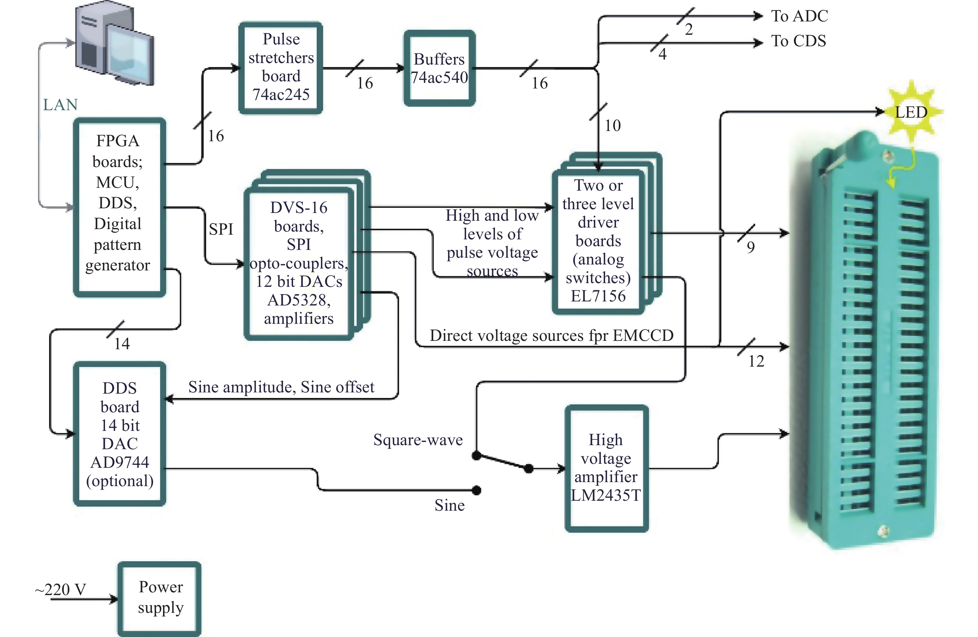
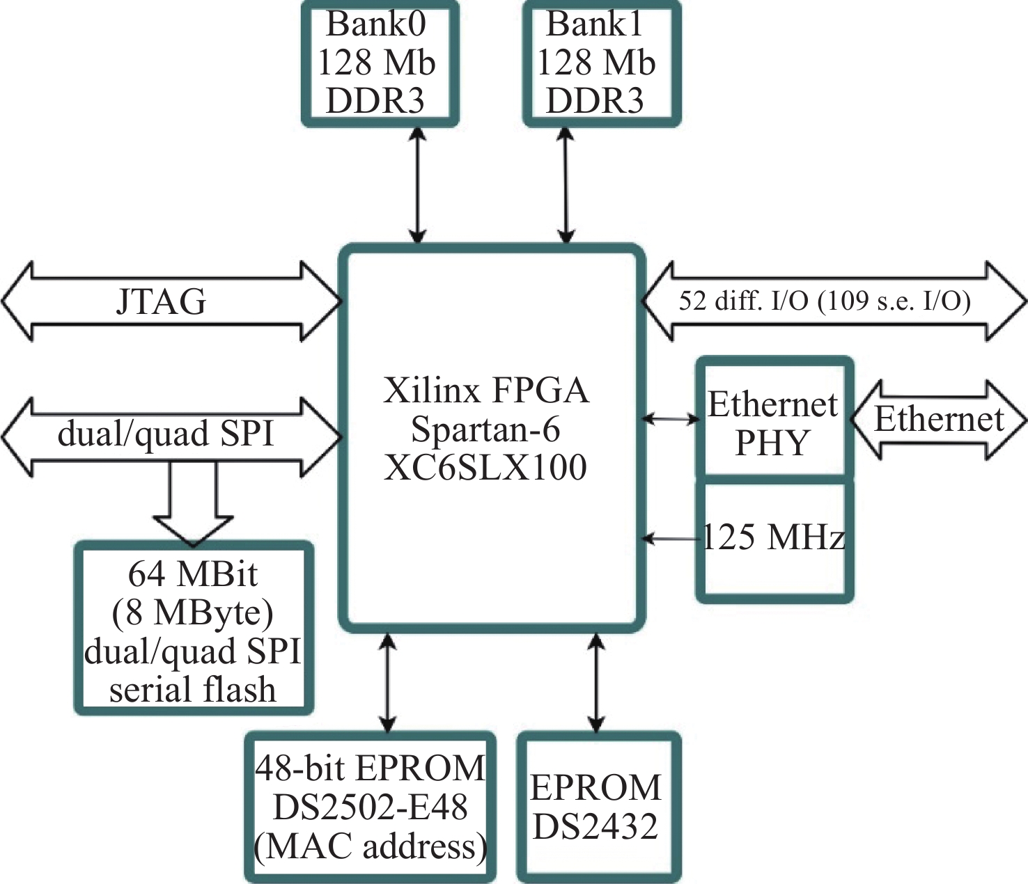
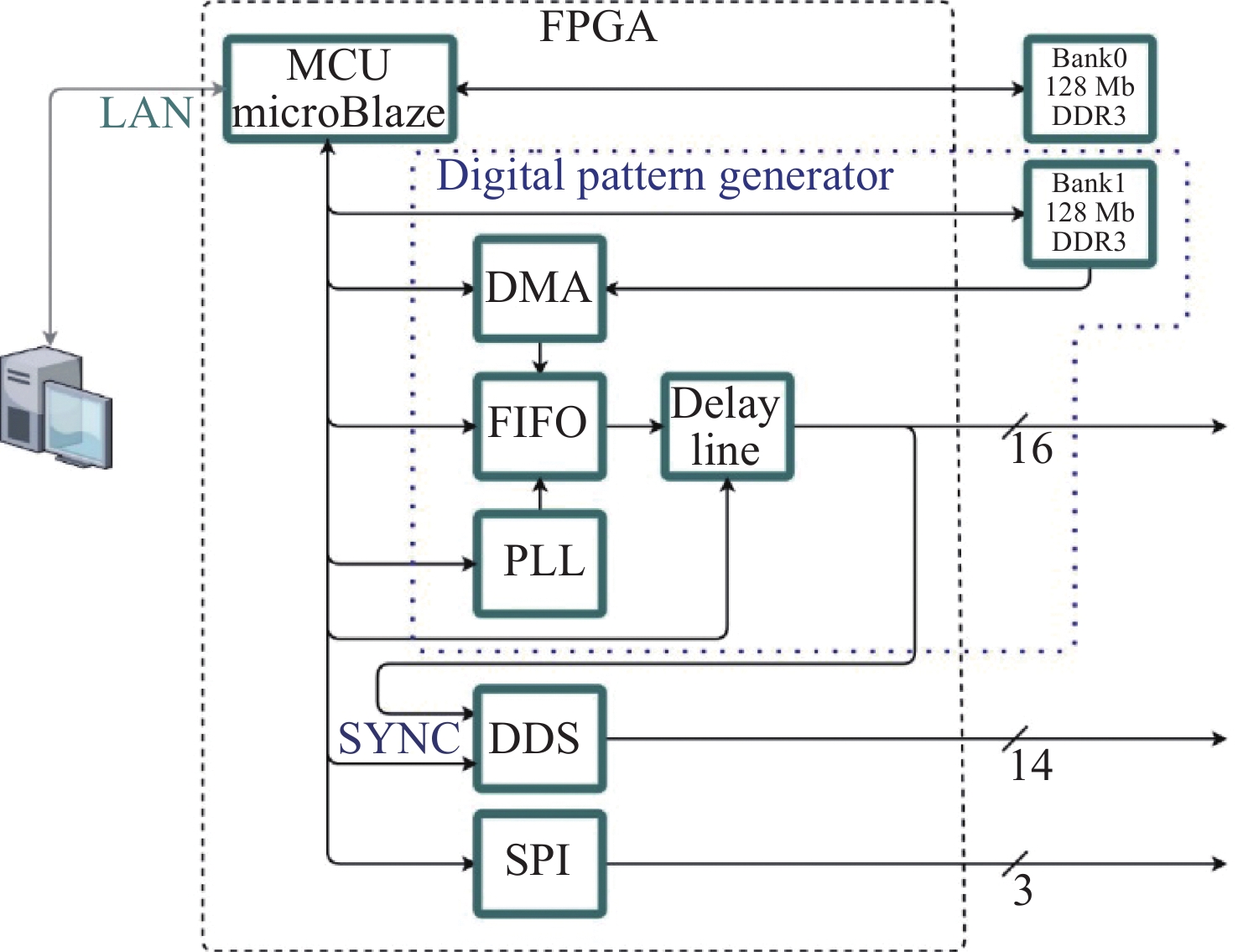
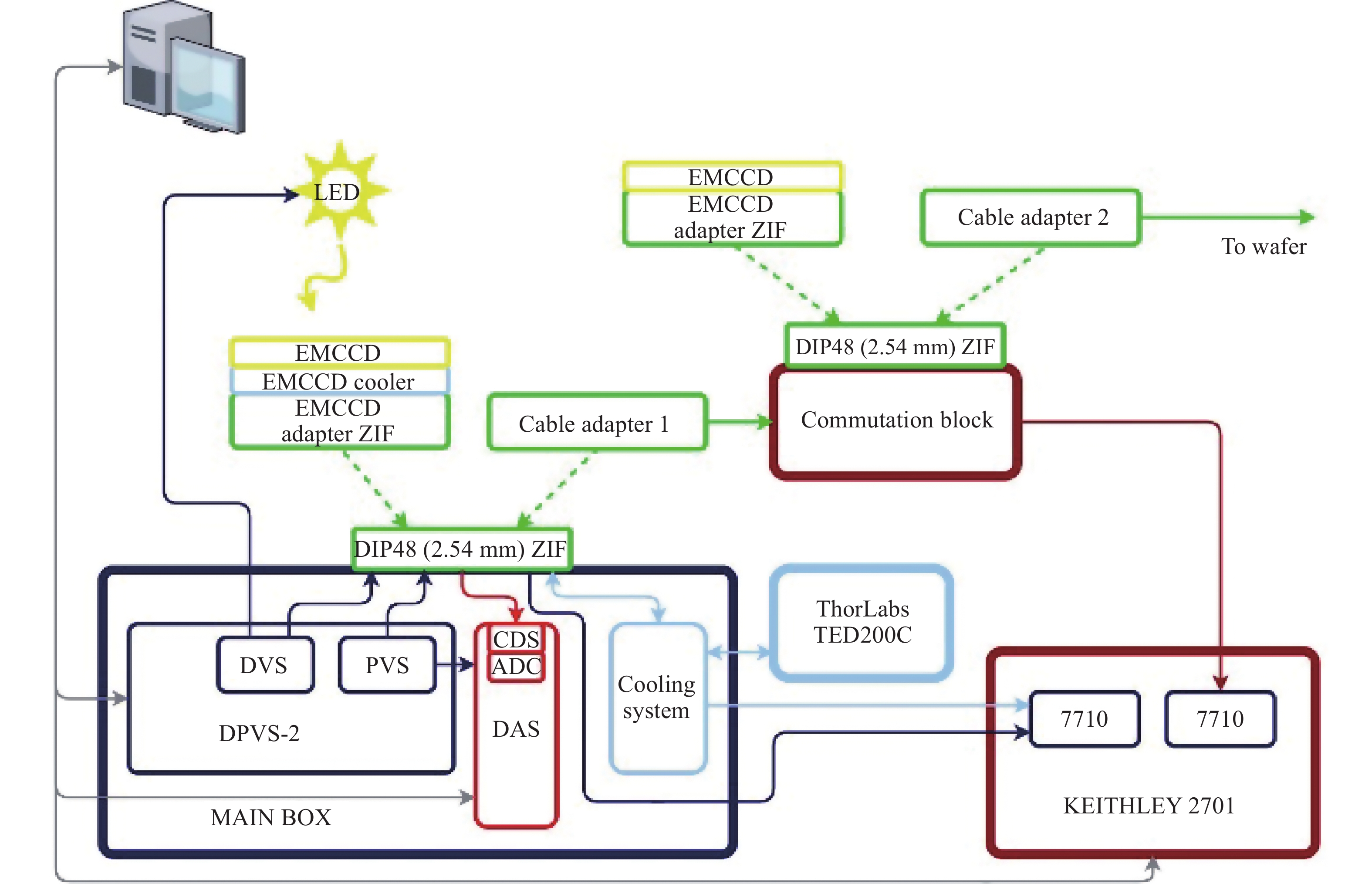
本文开发了一种用于测量CCD和EMCCD(电子倍增CCD)芯片光电参数的测试系统。该测试系统通过自动模式或手动模式间的切换测量器件的暗电流、读出放大器的响应度、电荷转移效率、电荷容量和其他参数。该测试系统可以针对不同规格和结构的CCD/EMCCD器件,实现CCD晶圆或封装好的成品的参数测试,实现576×288、640×512、768×576、1024×1024、1280×1024 CCD/EMCCD的测试和筛选。
Abstract:A photoelectrical parameters test system of CCD and electron-multiplying charge-coupled device (EMCCD) chips is designed. The test system has automatic and manual modes, and it can test the dark currents, the output amplifier’s responsivity, charge transfer efficiency, charge capacity and other parameters. According to different specifications and structures of CCD/EMCCD devices, complete the parameter test of wafer or packaged product. The developed system was used for 576 × 288, 640 × 512, 768 × 576, 1024 × 1024, 1280 × 1024 CCD and EMCCD chip testing and sorting.
-
Key words:
- CCD /
- EMCCD /
- test system /
- photoelectrical parameters
-

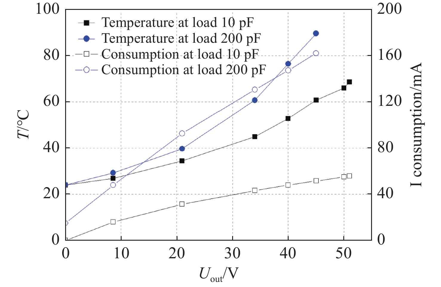
Figure 8. Driver’s power consumption and temperature at different output voltage and load.

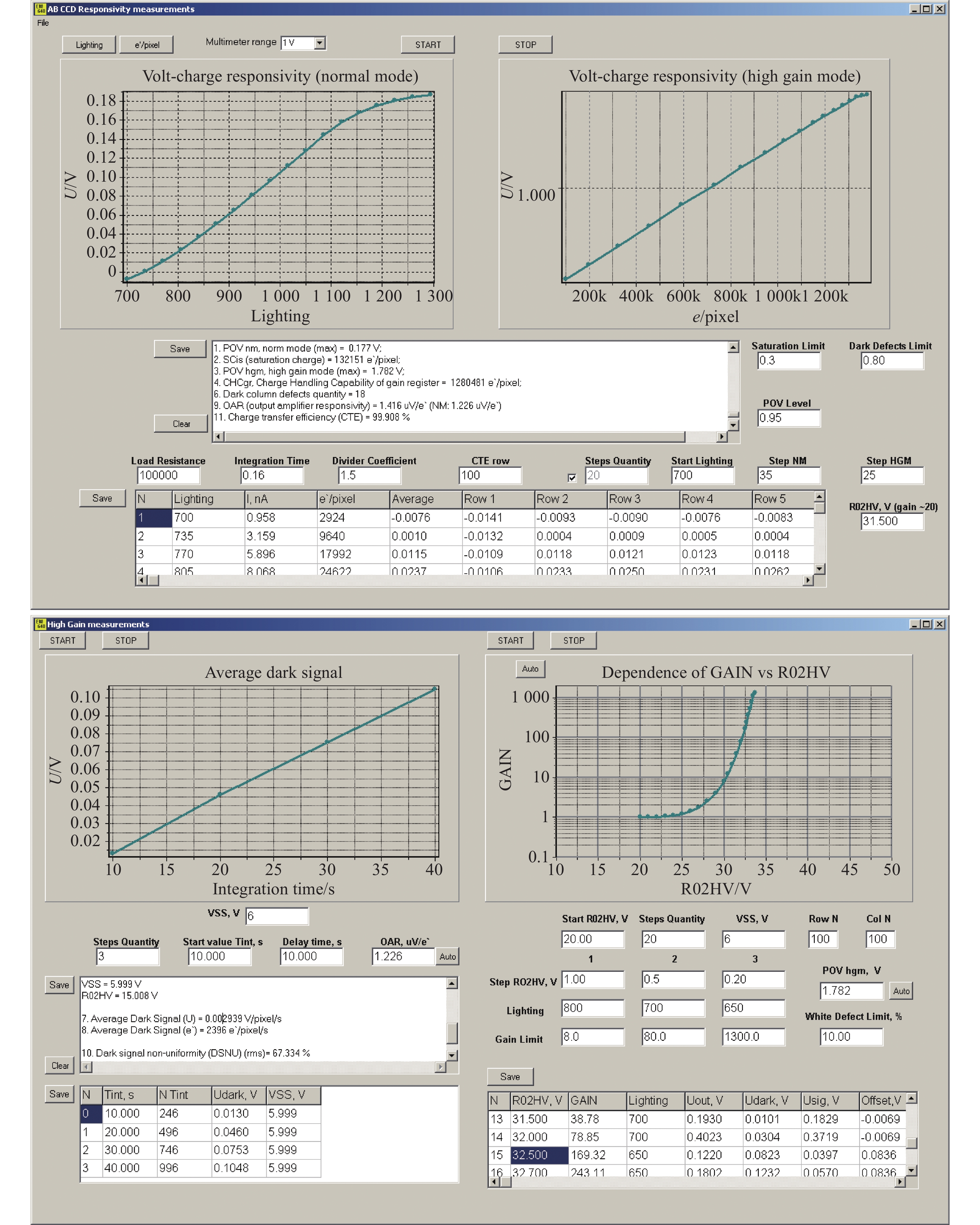
Figure 9. Flow chart for measuring maximum output voltage, charge capacity, and output amplifier responsivity.

Figure 10. Measuring results of test system. Volt-charge responsivity for normal and gain modes, average dark signal, and dependence of gain vs. R02HV voltage were measured
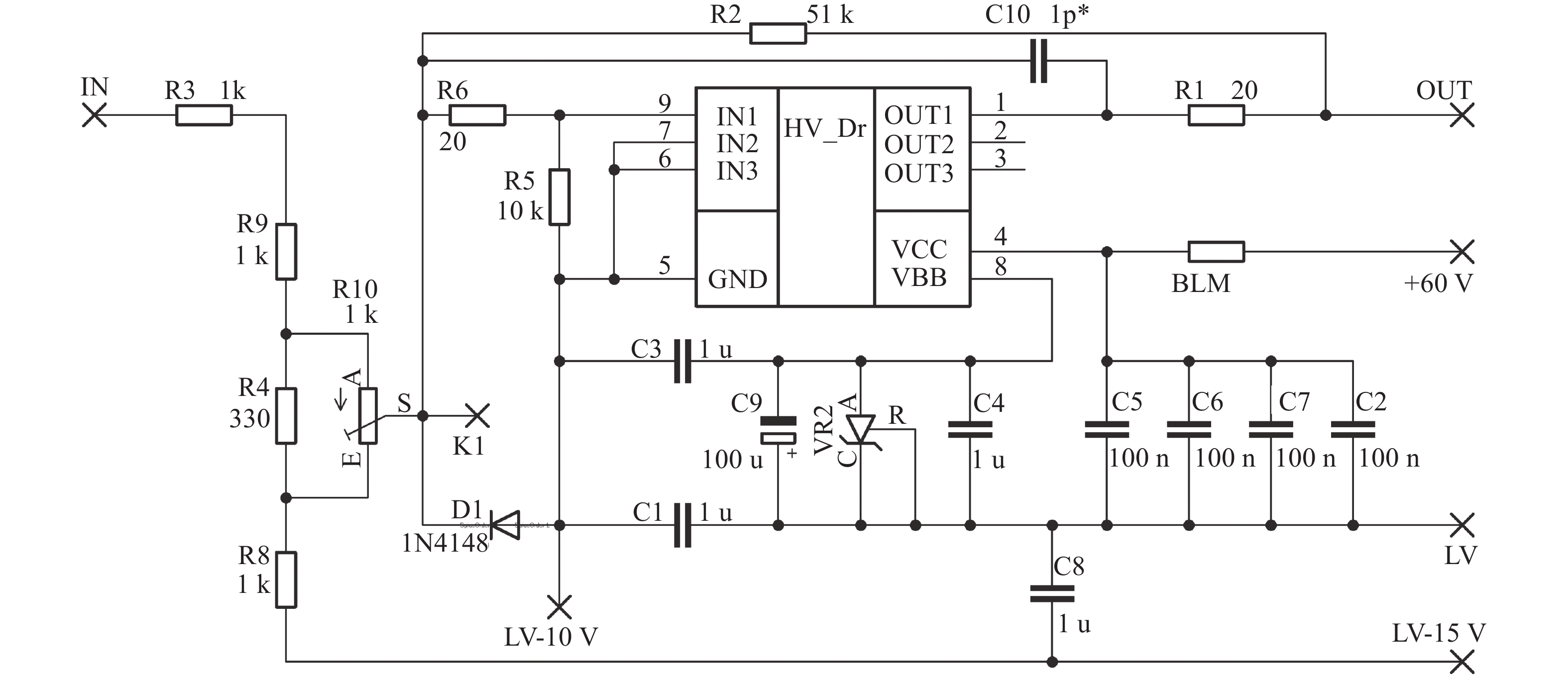
Table 1. Parameters of 16 DC channels
Channel
quantitySetting range/
VTotal relative
errorNoise,
mV/300 kHz1 −5···+10 typical: ±0.1%;
maximal: ±0.5%
from Vmax<0.15 3 0···+15 < 0.15 4 −5···+15 < 0. 20 4 0···+25 < 0.40 4 0···35 < 0.70  下载: 导出CSV
Table 2. Parameters of 16 AC channels
Channel quantity Setting range/ V Wave front/ ns Load (each channel) 3 HL, LL: –5...+10 120..200 up to 24 nF 4 HL: –5...+10 or 0...+15
LL: –5...+10 or 0...+15< 15 220 pF 1 HL: 0...+15
LL: 0...+15< 15 220 pF 6 HL: +5
LL: 0< 5 150 pF 1 HL: –5...+ 15;
LL, ML: –5...+10
(three level signal)120..200 up to 24 nF 1 HL: –5...+45
LL: –5...+ 45
(square or sine wave)20 100 pF
下载: 导出CSV
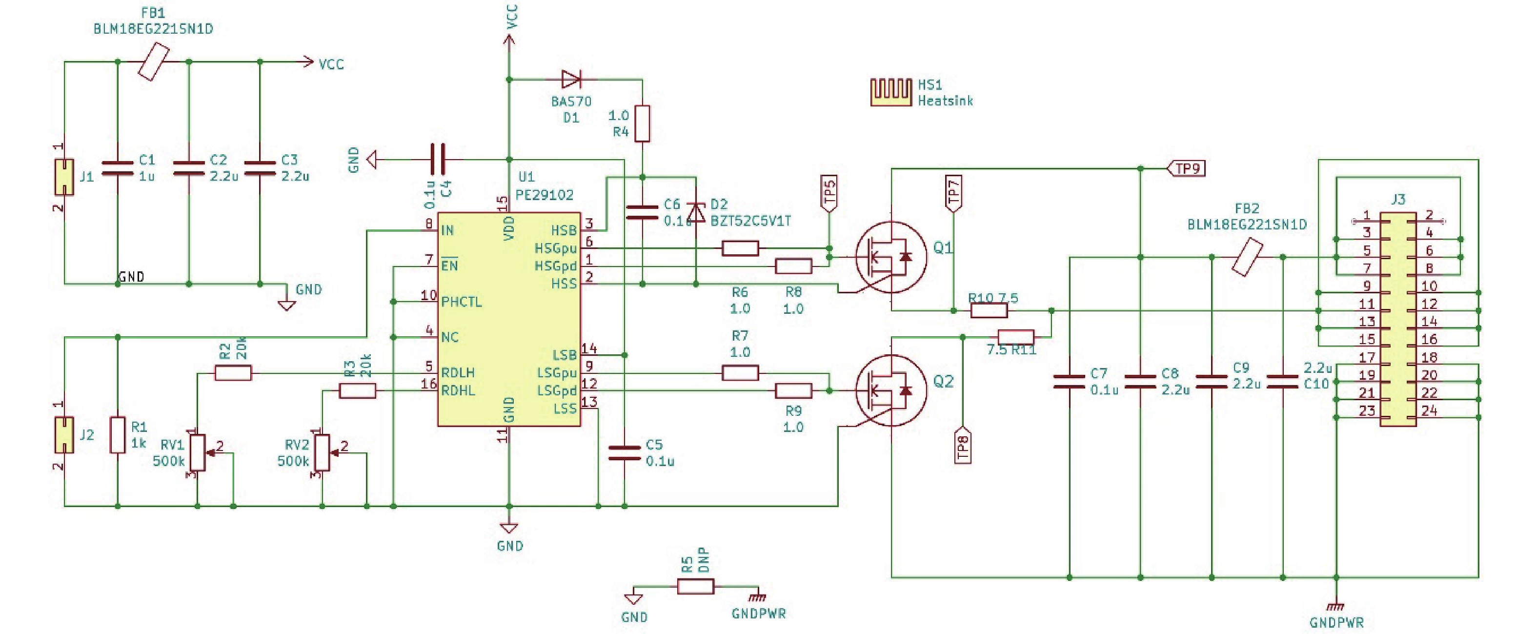
Table 3. Electrical parameters of EMCCD matrices measurable by the test system
No Parameter Range 1 Resistances between the pairs of chip contact pads 2 Average Dark Signal > 1 e/pixel/s 3 Dark Signal Non-uniformity (DSNU) 4 Multiplication Gain 1~1000 5 Peak Output Voltage (POV) < 1 V 6 Output Amplifier Responsivity (OAR) μV/e- 7 Register Charge Handling 8 Electric Charge Transfer Efficiency (CTE) ≤ 0.99995
下载: 导出CSV
Table 4. Measurements example of test system
1. POV nm, norm mode (max) = 0.177 V; 2. SC is (saturation charge) = 132151 e`/pixel; 3. POV hgm, high gain mode (max) = 1.782 V; 4. CHCgr, Charge Handling Capability of gain
register = 1280481 e`/pixel;5. White column defects = 3 6. Dark column defects quantity = 18 7. Average Dark Signal (U) = 0.002939 V/pixel/s 8. Average Dark Signal (e`) = 2396 e`/pixel/s 9. OAR (output amplifier responsivity) = 1.416 uV/e` (NM: 1.226 uV/e`) 10. Dark signal non-uniformity (DSNU) (rms) = 67.334 % 11. Charge transfer efficiency (CTE) = 99.908 %
下载: 导出CSV
-
[1] DENVIR D J, CONROY E. Electron-multiplying CCD: The new ICCD[C]. Proceedings of the SPIE 4796, Low-Light-Level and Real-Time Imaging Systems, Components, and Applications, SPIE, 2003: 164-174,doi: 10.1117/12.457779. [2] ROBBINS M S, HADWEN B J. The noise performance of electron multiplying charge-coupled devices[J]. IEEE Transactions on Electron Devices, 2003, 50(5): 1227-1232. doi: 10.1109/TED.2003.813462 [3] BOGAART E W, HOEKSTRA W, PETERS I M, et al. Very low dark current CCD image sensor[J]. IEEE Transactions on Electron Devices, 2009, 56(11): 2462-2467. doi: 10.1109/TED.2009.2030642 [4] SEITZ P, THEUWISSEN A J P. Single-Photon Imaging[M]. Berlin: Springer, 2011: 354. [5] SHIMIZU R, ARIMOTO M, NAKASHIMA H, et al. A charge-multiplication CMOS image sensor suitable for low-light-level imaging[J]. IEEE Journal of Solid-State Circuits, 2009, 44(12): 3603-3608. doi: 10.1109/JSSC.2009.2035541 [6] BRUGIÈRE T, MAYER F, FEREYRE P, et al. A theory of multiplication noise for electron multiplying CMOS image sensors[J]. IEEE Transactions on Electron Devices, 2014, 61(7): 2412-2418. doi: 10.1109/TED.2014.2320966 [7] STEFANOV K D, DUNFORD A, HOLLAND A D. Electron multiplying low-voltage CCD with increased gain[J]. IEEE Transactions on Electron Devices, 2018, 65(7): 2990-2996. doi: 10.1109/TED.2018.2839023 [8] WILKINS A N, MCELWAIN M W, NORTON T J, et al. Characterization of a photon counting EMCCD for space-based high contrast imaging spectroscopy of extrasolar planets[C]. Proceedings of the SPIE 9154, High Energy, Optical, and Infrared Detectors for Astronomy VI, SPIE, 2014: 91540C,doi: 10.1117/12.2055346. [9] DUSSAULT D, HOESS P. Noise performance comparison of ICCD with CCD and EMCCD cameras[C]. Proceedings of the SPIE 5563, Infrared Systems and Photoelectronic Technology, SPIE, 2004: 195-204,doi: 10.1117/12.561839. [10] SOESBE T C, LEWIS M A, RICHER E, et al. Development and evaluation of an EMCCD based gamma camera for preclinical SPECT imaging[J]. IEEE Transactions on Nuclear Science, 2007, 54(5): 1516-1524. doi: 10.1109/TNS.2007.906408 [11] REVA V P, KORINETS S V, GOLENKOV A G, et al. CCD Photomatrixes with electron multiplication[J]. Технология и Конструирование в Электронной Аппаратуре, 2017(1-2): 33-37,doi: 10.15222/TKEA2017.1-2.33. (查阅网上资料,未能确认刊名修改是否正确,请确认) . [12] WU Q, FENG Z H, LI X W. Design and test of an EMCCD CCD201 sensor driving circuit[C]. Proceedings of the International Conference on Communication and Electronic Information Engineering, Atlantis Press, 2017: 319-326,doi: 10.2991/ceie-16.2017.40. [13] HOPE S C, GUNN J E, LOOMIS C P, et al. CCD readout electronics for the subaru prime focus spectrograph[C]. Proceedings of the SPIE 9154, High Energy, Optical, and Infrared Detectors for Astronomy VI, SPIE, 2014: 91542G,doi: 10.1117/12.2057166. [14] RYAN D P, DUNLAP M K, GELFAND M P, et al. A gain series method for accurate EMCCD calibration[J]. Scientific Reports, 2021, 11(1): 18348. doi: 10.1038/s41598-021-97759-6 [15] PE29102: Product specification[EB/OL].https://www.psemi.com/pdf/datasheets/pe29102ds.pdf. (查阅网上资料,未找到本条文献日期信息,请确认) . [16] Using peregrine’s high-speed FET drivers[EB/OL].https://www.psemi.com/pdf/app_notes/an71.pdf. (查阅网上资料,未找到本条文献日期信息,请确认) . -

 下载:
下载:


 点击查看大图
计量
- 文章访问数: 221
- HTML全文浏览量: 61
- PDF下载量: 38
- 被引次数: 0
