


-
摘要:
为了突破目前热光波导光开关开关速度慢、热量易积累、器件功耗高,电光波导光开关传输损耗高,以及现有传统光子集成电路波导光开关器件普遍存在的反馈控制复杂、难以实现大阵列规模应用且工作带宽较窄等问题,以满足未来片上全光交换技术对快响应、低功耗、宽带、低成本、可实现大阵列规模制备应用的光开关器件为需求,开展基于微机电系统(Micro-Electro-Mechanical System, MEMS)驱动的硅基波导光开关器件研究。基于硅光波导技术和微机电技术交叉融合,设计并制备了一种可实现光信号路由功能的MEMS静电驱动2×2硅基波导光开关(硅光MEMS光开关)。通过电子束光刻配合互补氧化物金属半导体(Complementary Metal Oxide Semiconductor, CMOS)工艺实现硅光波导和MEMS微执行器在硅晶圆上的一体化集成制备。器件在192 μm×192 μm尺寸下实现了2×2光开关功能,开关响应速度达到20 μs及15 μs,光信号上升沿及下降沿时间分别为15 μs和10 μs。在
1550 nm消光比达到35 dB,插入损耗为−0.8 dB,在1500 nm~1600 nm波段消光比超过20 dB,器件在开启状态的保持功耗低于0.5 μW。测试结果表明该硅光MEMS光开关响应速度快、调制功耗低、宽带性能良好,在现有工艺平台下可实现大规模阵列化制备且控制方式简单,在未来片上全光交换领域具有较大的应用价值。Abstract:To overcome the limitations of current technologies, including the slow switching speed, heat accumulation, and high power consumption of thermo-optic waveguide switches, the high transmission loss of electro-optic waveguide switches, and the complex feedback control, difficulty in large-scale array integration, and narrow operating bandwidth commonly found in traditional photonic integrated circuit (PIC) waveguide switches, to meet the future demands of on-chip all-optical switching technologies for optical switches with fast response, low power consumption, broad bandwidth, low cost, and large-scale array fabrication capabilities, this study investigates micro-electro-mechanical systems (MEMS) driven silicon-based waveguide optical switch devices. By integrating silicon photonic waveguide technology with MEMS technology, we designed and fabricated an electrostatically driven MEMS 2×2 silicon waveguide optical switch (silicon photonic MEMS switch) capable of routing optical signals. The monolithic integration of silicon photonic waveguides and MEMS microactuators on a silicon wafer was achieved using electron-beam lithography combined with complementary metal-oxide-semiconductor (CMOS) processes. With a footprint of 192 μm × 192 μm, the device successfully demonstrated 2×2 optical switching functionality. The switching response times were measured at 20 μs and 15 μs, with optical signal rise and fall times of 15 μs and 10 μs, respectively. At a wavelength of
1550 nm, the device achieved an extinction ratio (ER) of 35 dB and an insertion loss (IL) of −0.8 dB. Over the1500 –1600 nm wavelength band, the ER remained above 20 dB, and the holding power consumption in the ON state was less than 0.5 μW. Experimental results demonstrate that this silicon photonic MEMS optical switch features fast response, low modulation power consumption, and excellent broadband performance. Furthermore, it can be fabricated into large-scale arrays with simple control mechanisms using existing process platforms, indicating significant application potential in future on-chip all-optical switching networks. -
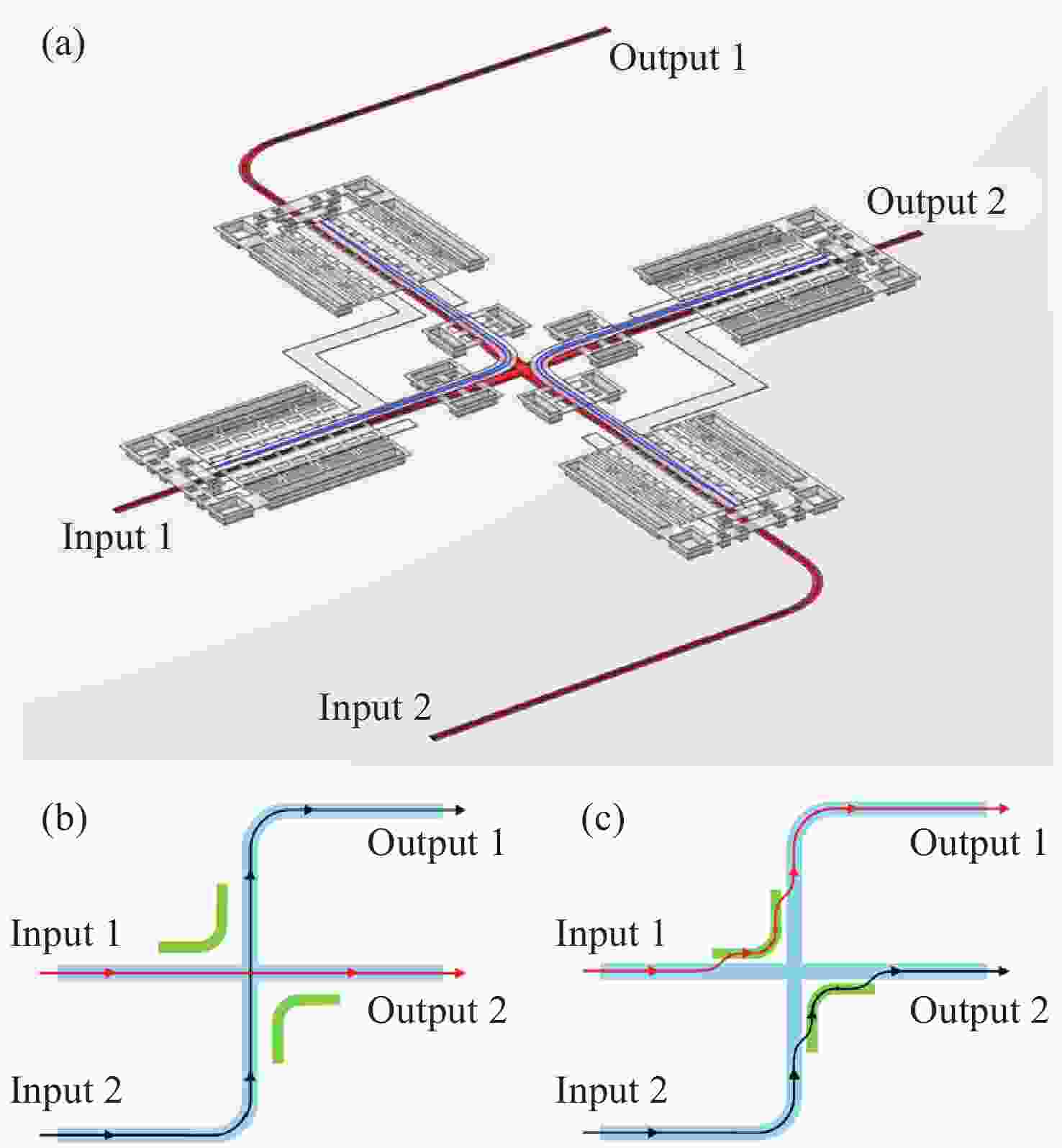
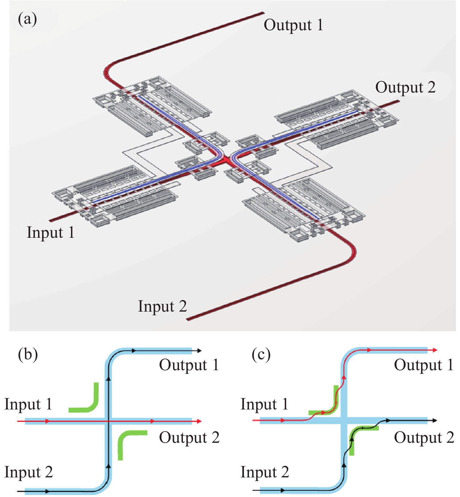
图 1 2×2 MEMS光开关工作原理。(a)三维结构;(b)关闭状态下光信号传输路径;(c)开启状态下光信号传输路径。
Figure 1. Working principle of a 2×2 MEMS optical switch. (a) 3D structure; (b) Optical signal transmission path in the OFF state; (c) Optical signal transmission path in the ON state.
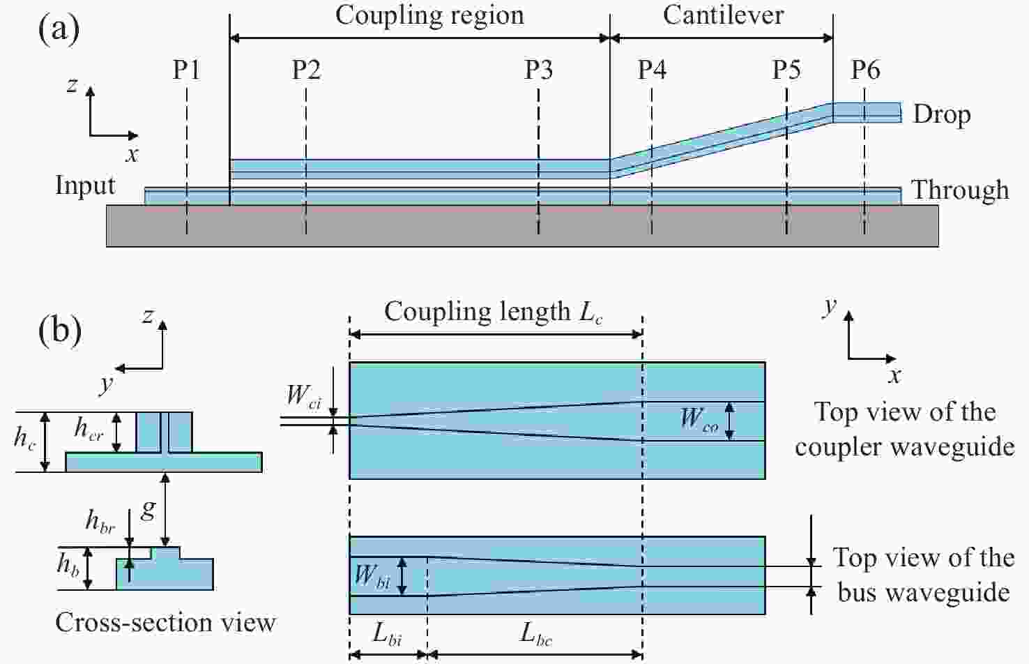
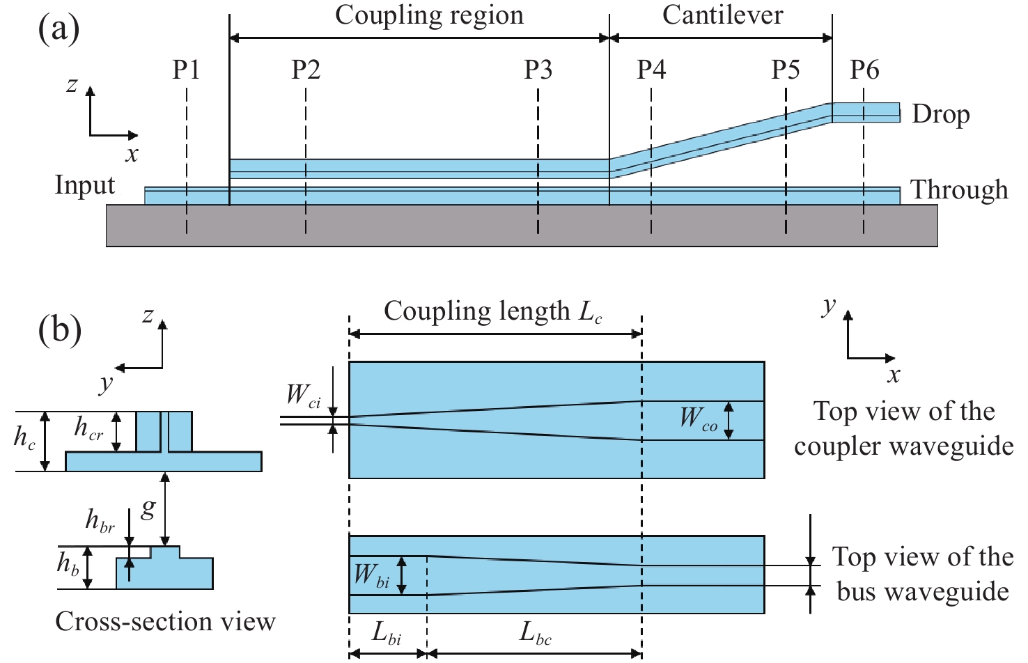
图 2 垂直耦合波导结构工作原理。(a)开启状态示意图;(b)耦合区域波导几何结构。
Figure 2. Working principle of the vertical coupling waveguide structure. (a) Schematic diagram of the ON state; (b) Geometric structure of the coupling region waveguide.
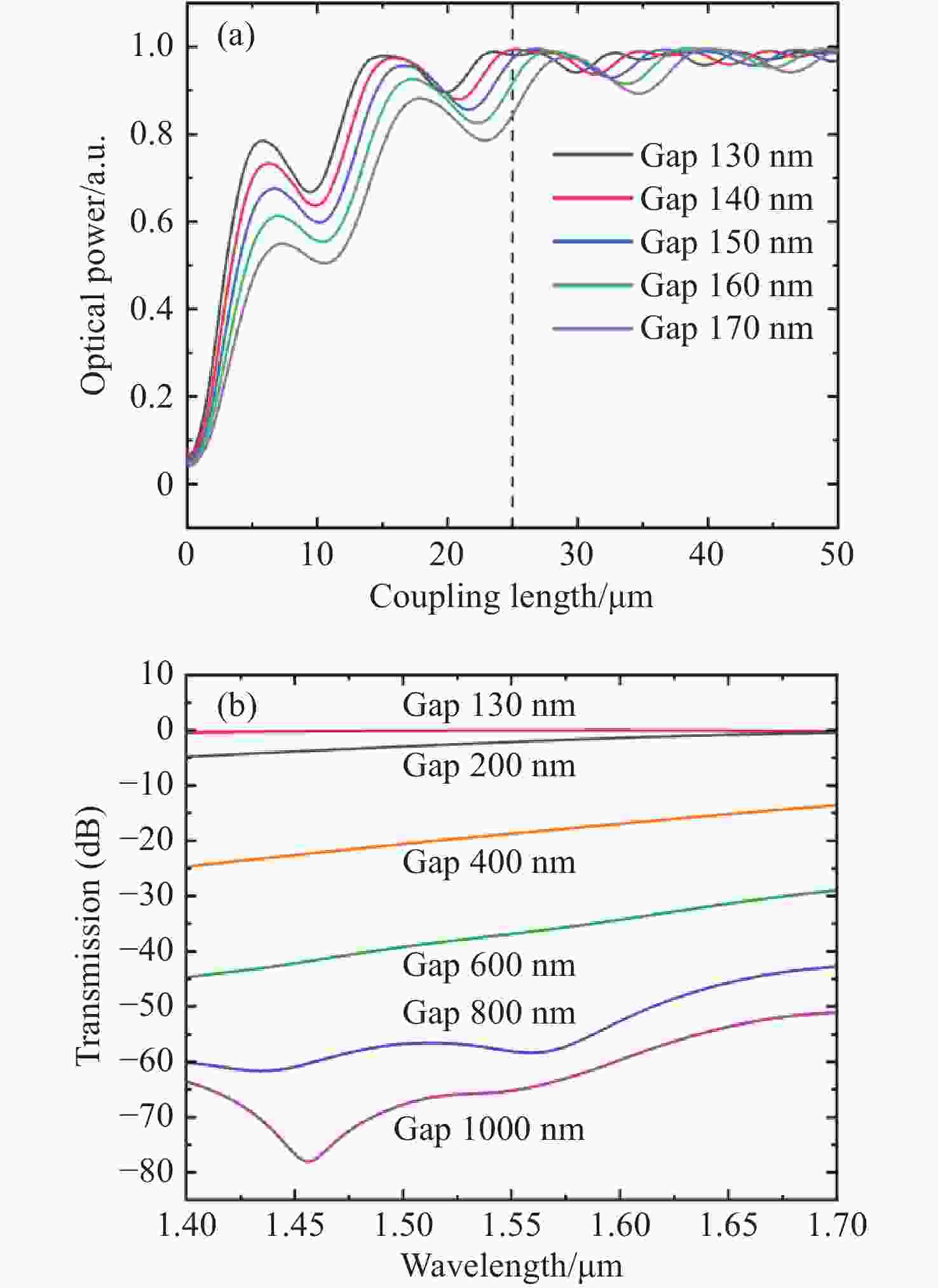
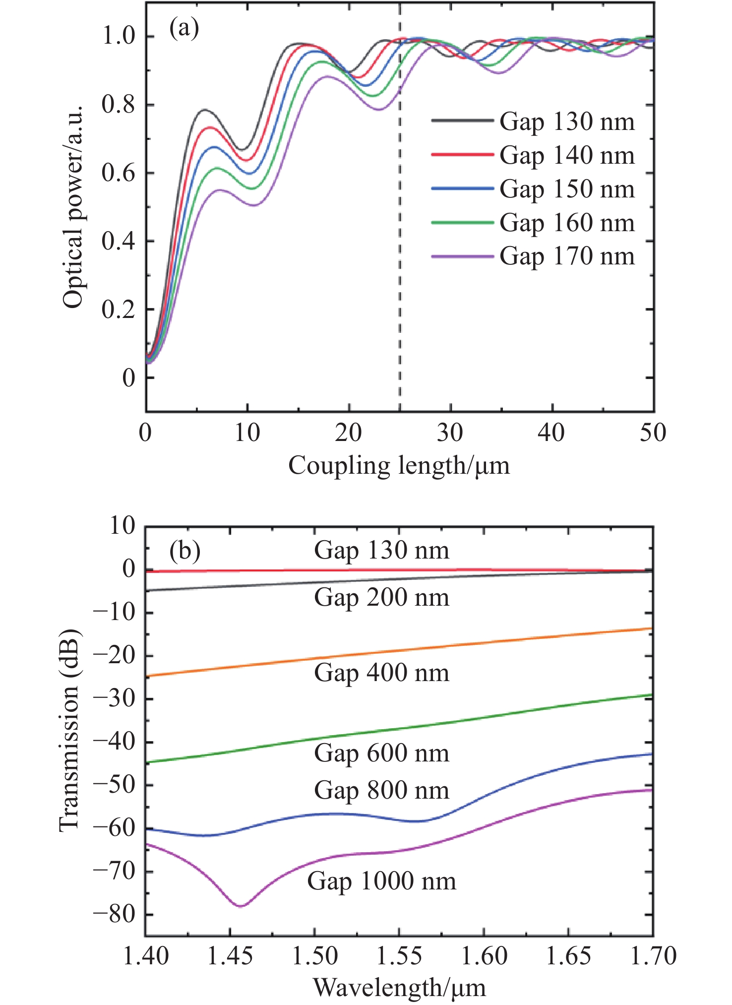
图 3 垂直耦合波导结构仿真设计。(a)不同耦合间隔下
1550 nm耦合效率随耦合长度变化曲线;(b)耦合长度25 μm时不同间隔的宽带耦合效率。Figure 3. Simulation design of the vertical coupling waveguide structure. (a) Coupling efficiency at
1550 nm versus coupling length under different coupling gaps; (b) Broadband coupling efficiency for various gaps with a coupling length of 25 μm.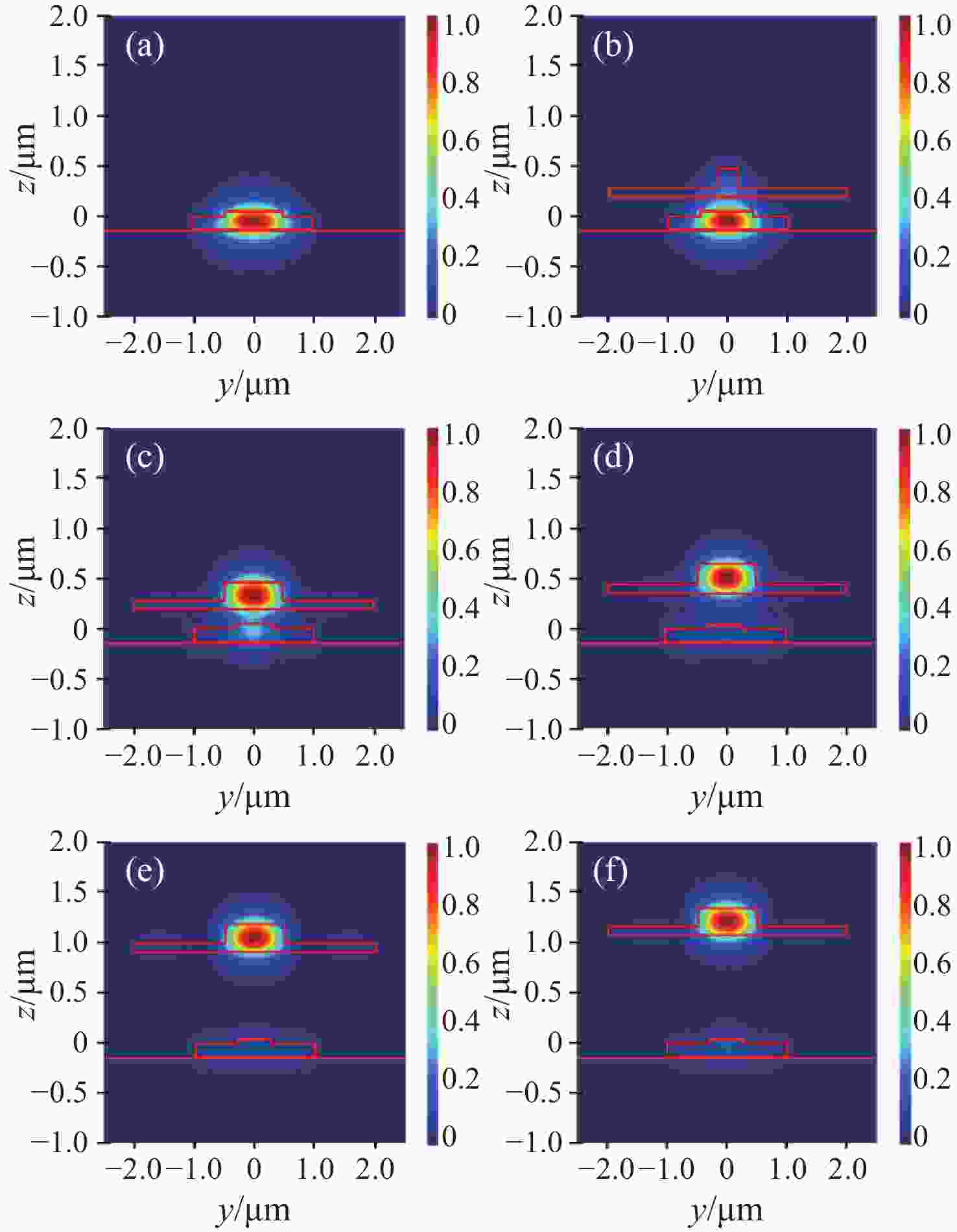
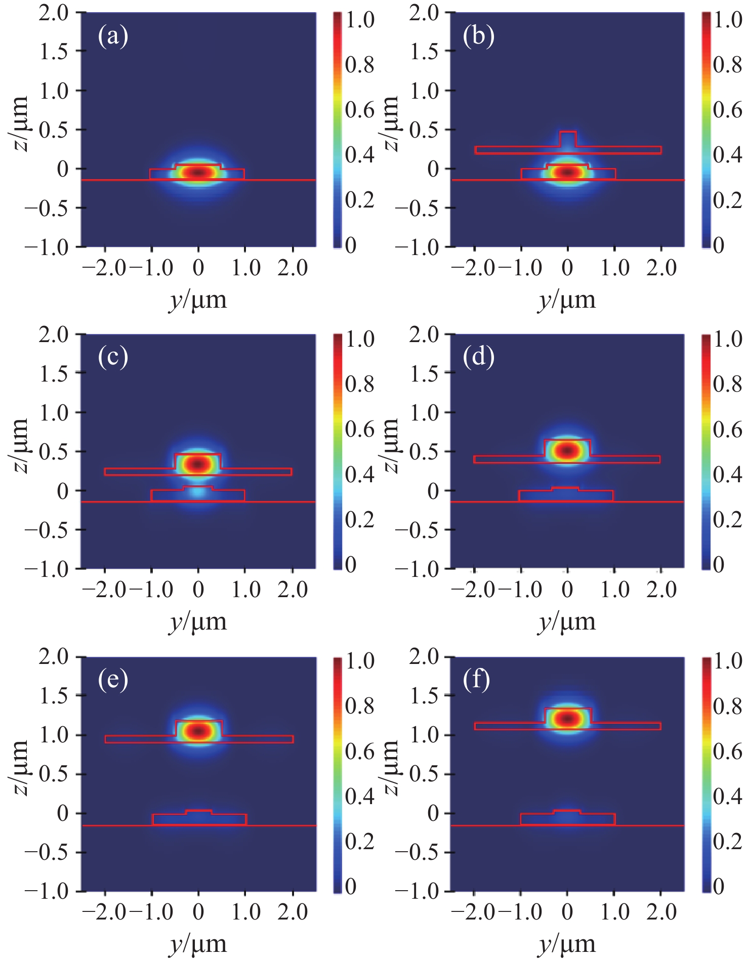
图 4 开启状态下垂直耦合波导结构光场分布。(a)输入端口(图2(a)中位置P1);(b)耦合区域起始端(图2(a)中位置P2);(c)耦合区域末端(图2(a)中位置P3);(d)悬臂梁起始端(图2(a)中位置P4);(e)悬臂梁末端(图2(a)中位置P5);(f)输出端口(图2(a)中位置P6)。
Figure 4. Optical field distribution of the vertical coupling waveguide structure in the ON state. (a) Input port (P1 in Fig. 2(a)); (b) Beginning of the coupling region (P2 in Fig. 2(a)); (c) End of the coupling region (P3 in Fig. 2(a)); (d) Beginning of the cantilever beam (P4 in Fig. 2(a)); (e) End of the cantilever beam (P5 in Fig. 2(a)); (f) Output port (P6 in Fig. 2(a)).
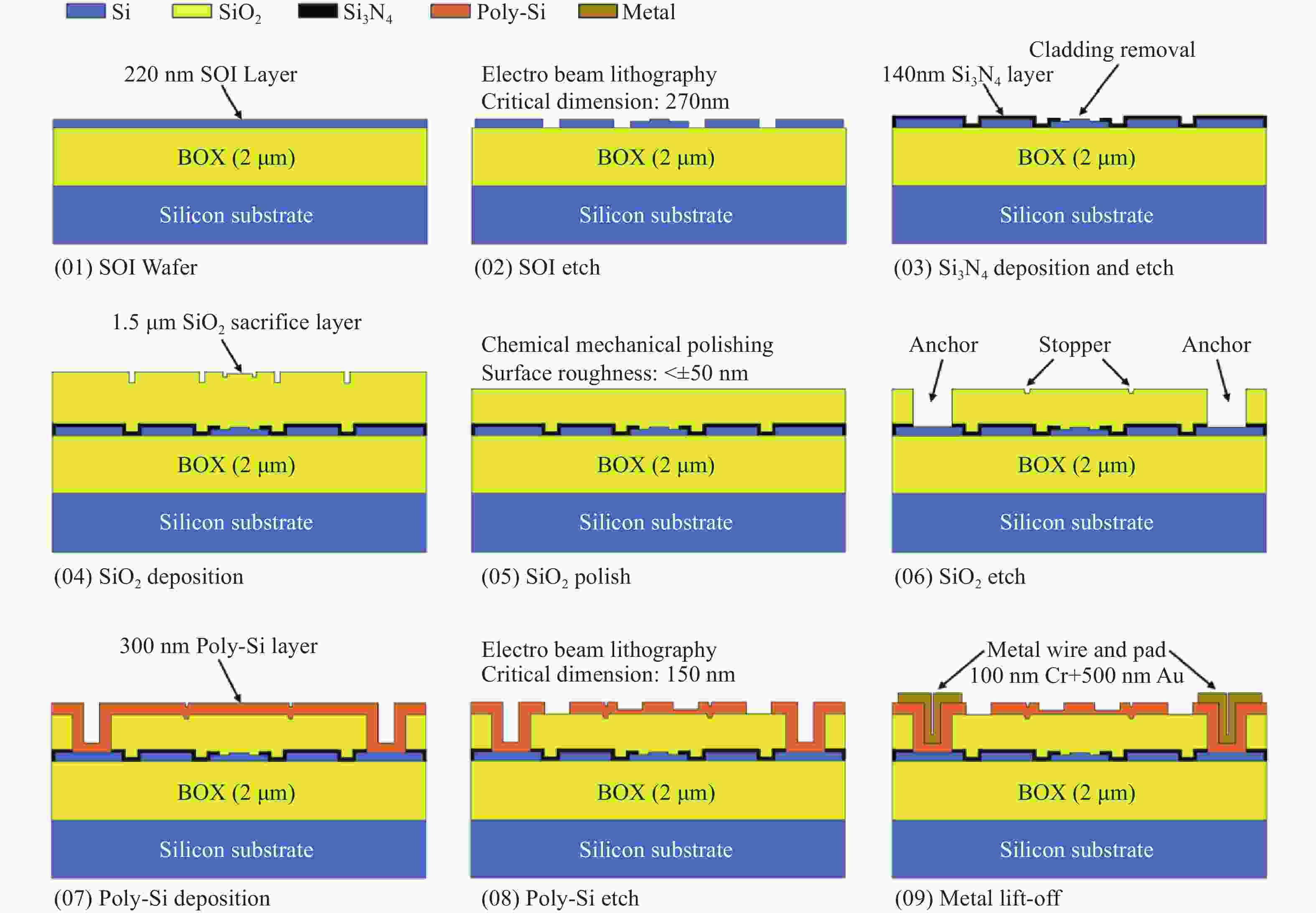
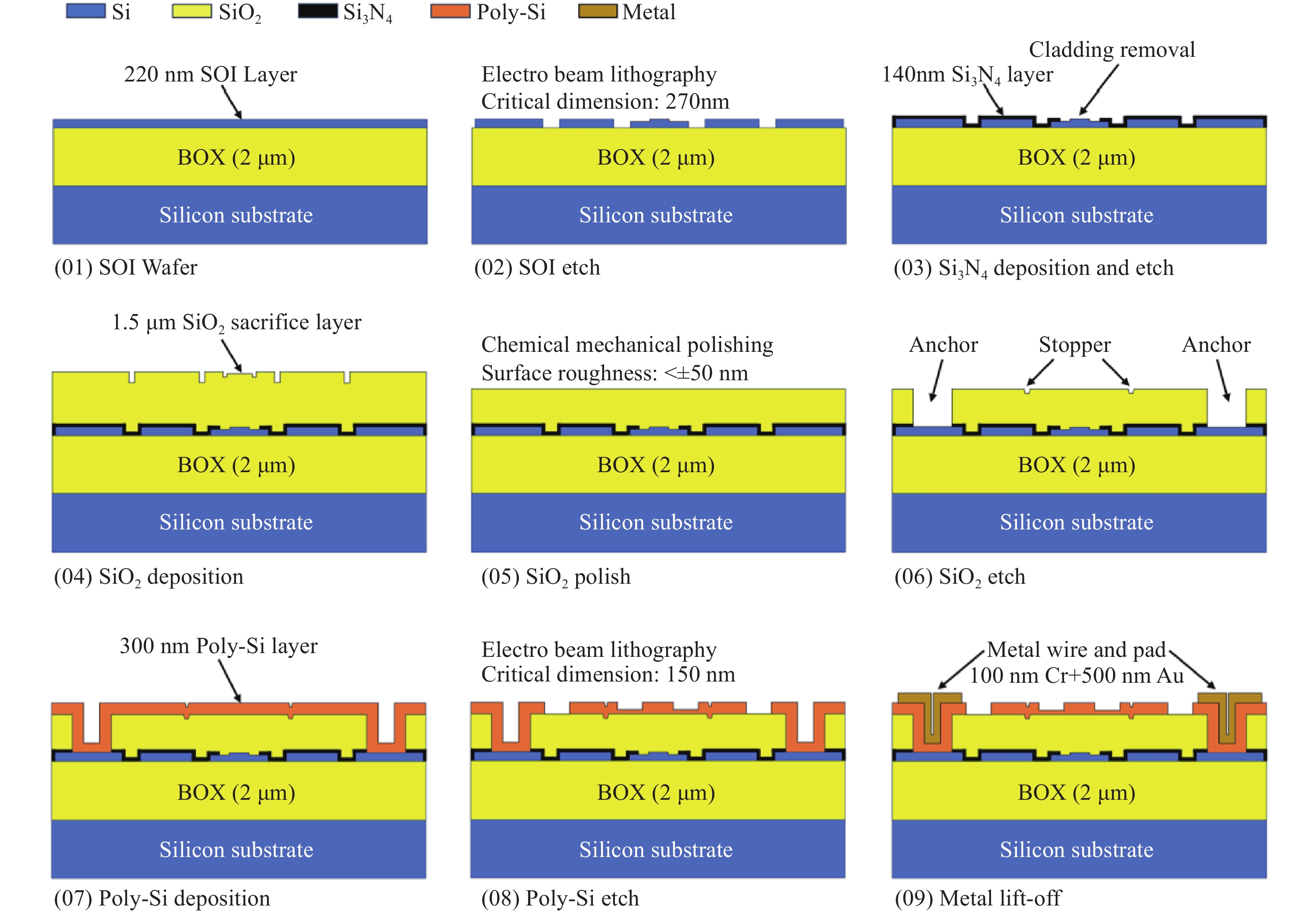
图 5 硅光MEMS波导光开关工艺流程。
Figure 5. Fabrication process of the silicon photonic MEMS waveguide optical switch.
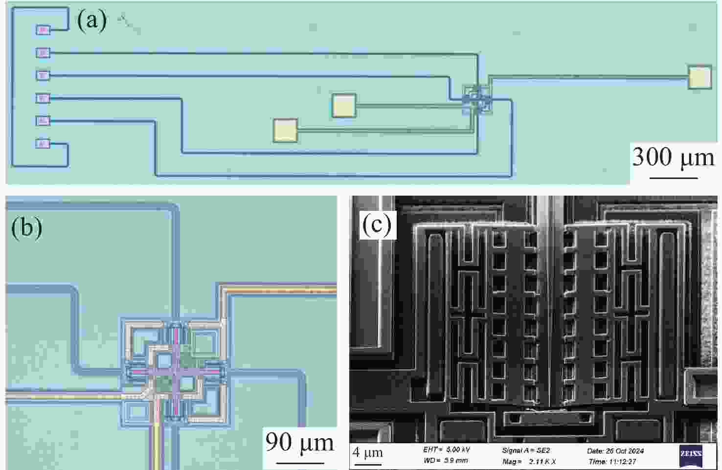
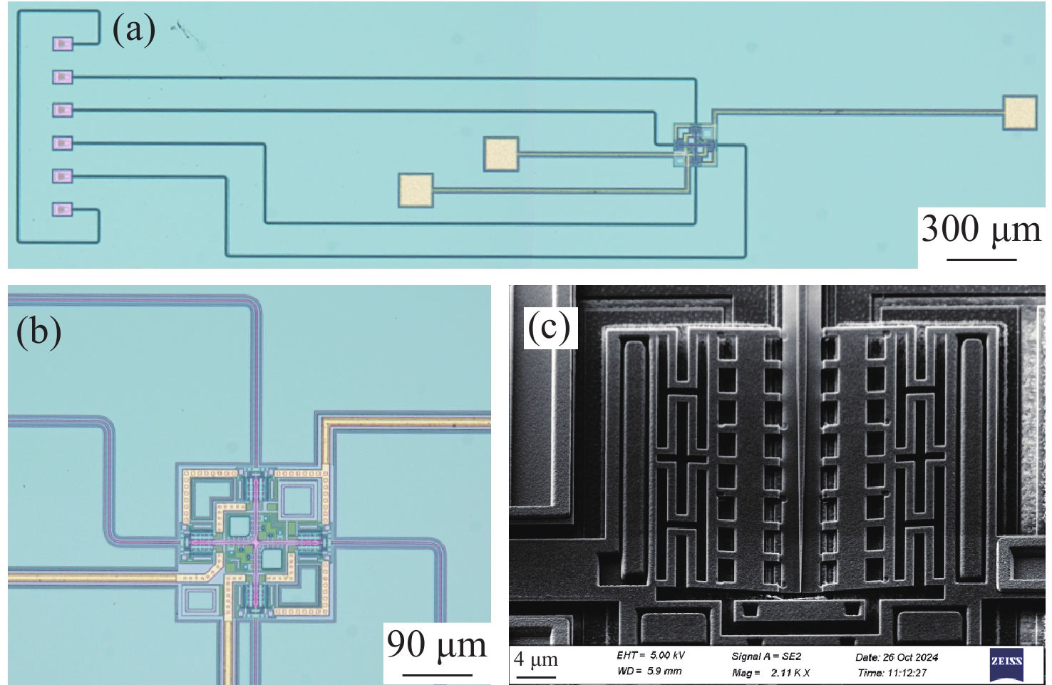
图 6 2×2硅光MEMS波导光开关。(a)器件整体结构光学显微镜图像;(b)硅光MEMS光学显微镜图像;(c)硅光波导和MEMS微执行器SEM图像。
Figure 6. 2×2 silicon photonic MEMS waveguide optical switch. (a) Optical microscope image of the overall device structure; (b) Optical microscope image of the silicon photonic MEMS; (c) SEM image of the silicon photonic waveguide and MEMS microactuator.
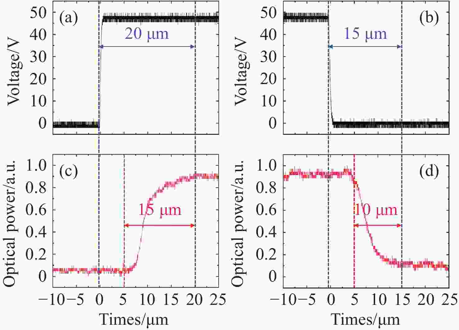
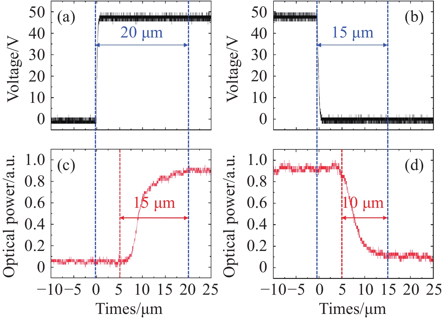
图 7 器件开关速度测试。(a)开启状态下开关响应时间和光信号上升沿时间;(b)关闭状态下开关响应时间和光信号下降沿时间。
Figure 7. Switching speed test of the device. (a) Switching response time and optical signal rise time in the ON-state; (b) Switching response time and optical signal fall time in the OFF-state.
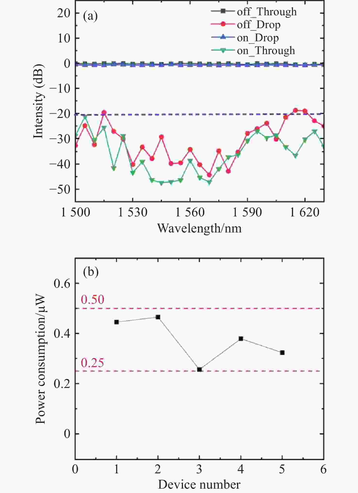
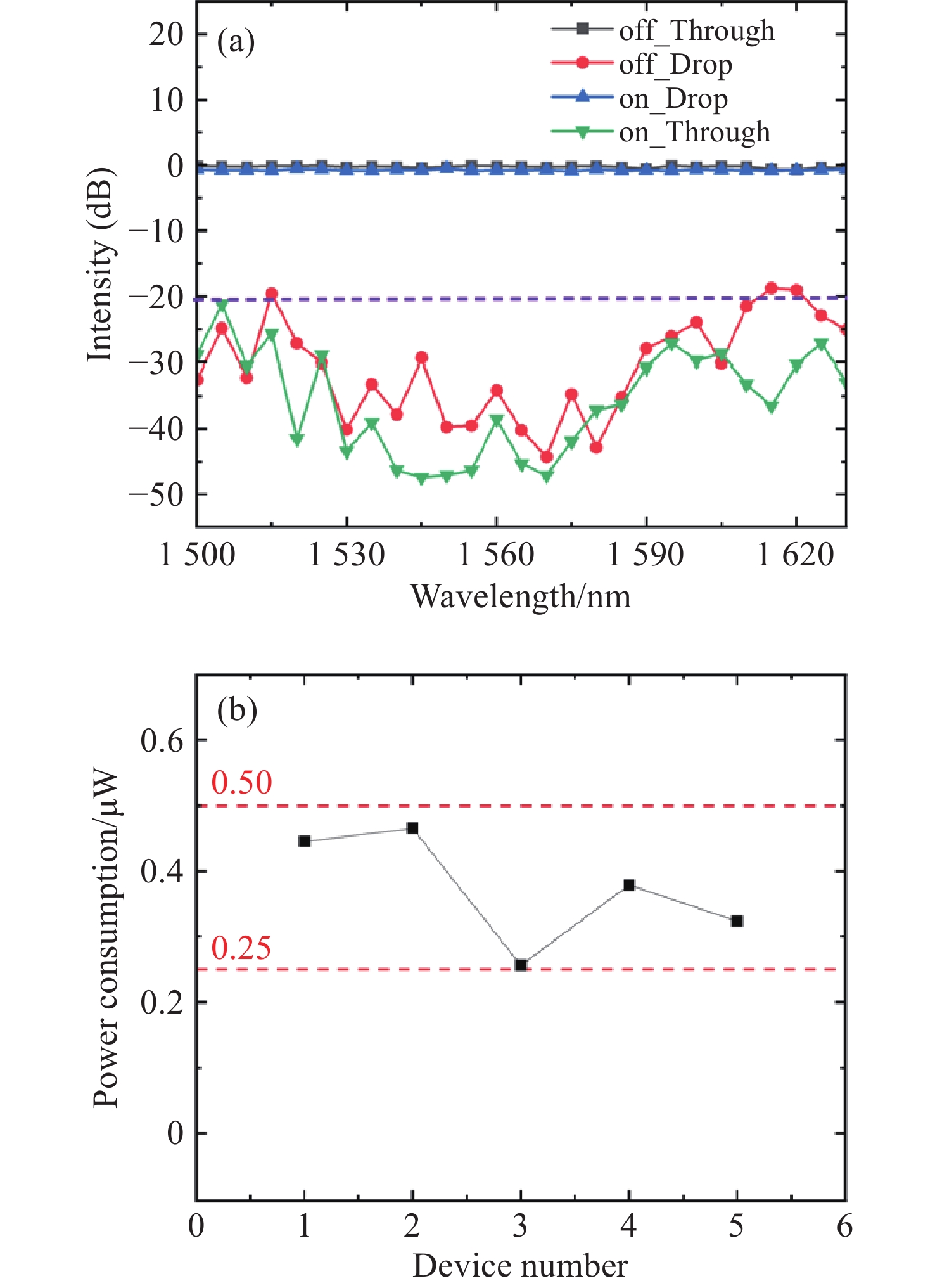
图 8 器件光学性能及功耗测试。(a)
1500 ~1620 nm波段光谱响应测试;(b)开启状态下的器件保持功耗测试。Figure 8. Optical performance and power consumption test of the device. (a) Spectral response test in the
1500 –1620 nm wavelength band; (b) Holding power consumption test in the ON state.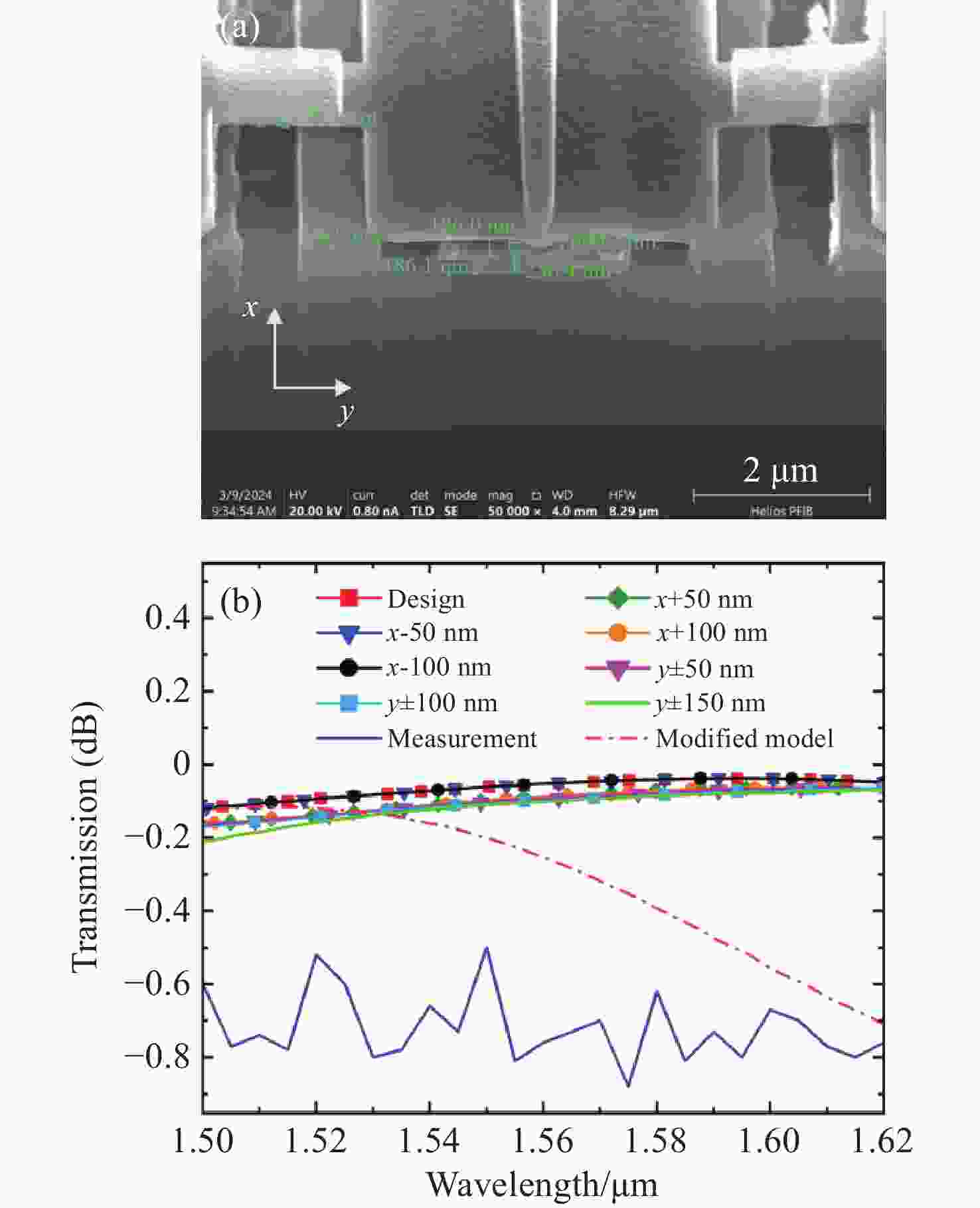
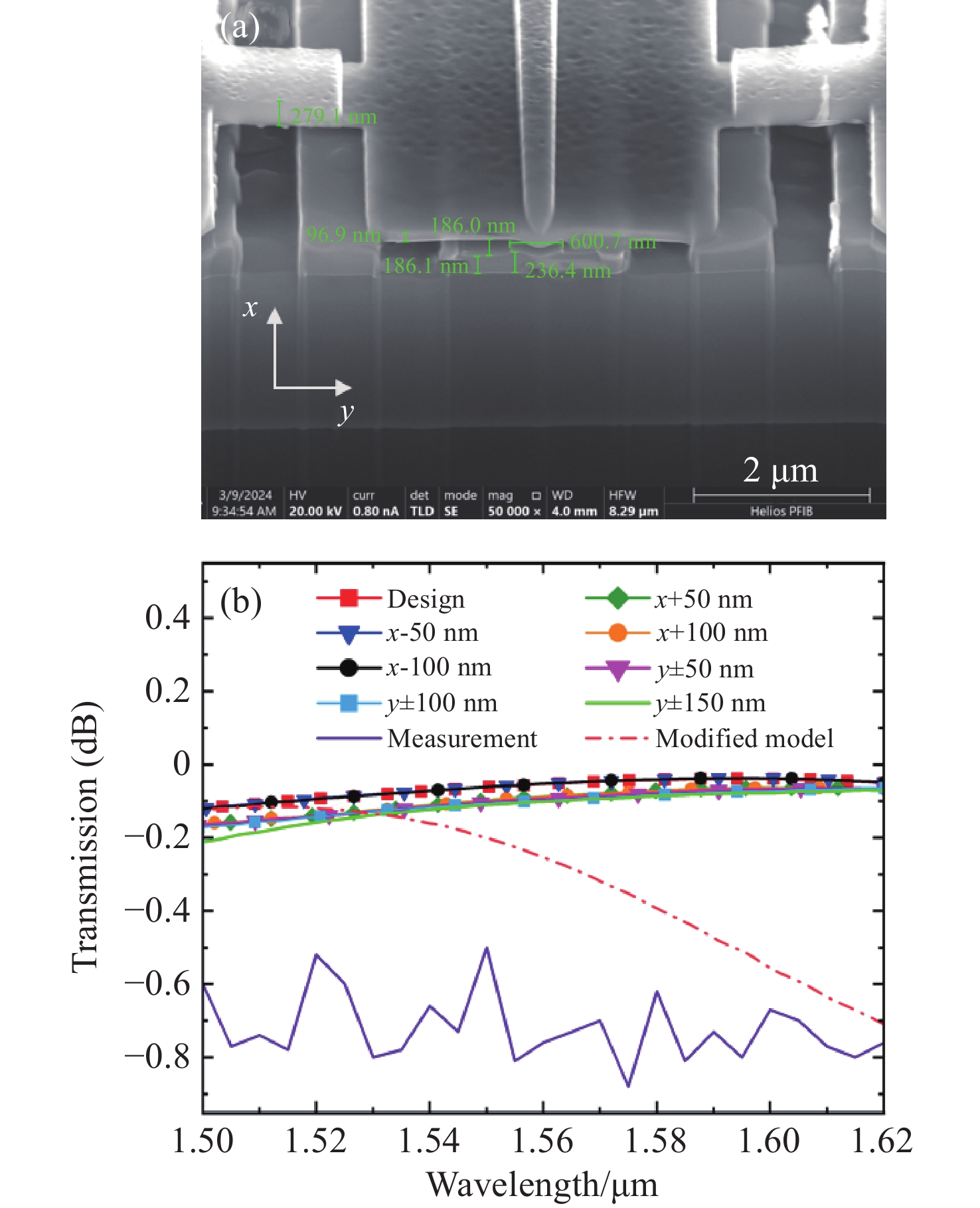
图 9 器件加工检验及仿真验证。(a) 硅光MEMS光开关剖面结构SEM图像;(b) 垂直耦合波导结构修正模型及工艺容差仿真。
Figure 9. Device fabrication inspection and simulation verification. (a) SEM image of the cross-sectional structure of the silicon photonic MEMS optical switch; (b) Modified model and process tolerance simulation of the vertical coupling waveguide structure.
-
[1] URATA R, LIU H, YASUMURA K, et al. Apollo: large-scale deployment of optical circuit switching for datacenter networking[C]. 2023 Optical Fiber Communications Conference and Exhibition (OFC), IEEE, 2023: 1-3. [2] URATA R, LIU H, YASUMURA K, et al. Mission Apollo: landing optical circuit switching at datacenter scale[J]. arXiv: 2208.10041, 2022. (查阅网上资料, 不确定文献类型及格式是否正确, 请核对). [3] WANG H, WANG ZH G, GONG CH, et al. Using light to image millimeter wave based on stacked meta-MEMS chip[J]. Light: Science & Applications, 2025, 14(1): 59. [4] RASTEGARFAR H. Optical switching in next-generation data centers[D]. Toronto: University of Toronto, 2014. (查阅网上资料, 未能确认本条文献修改是否正确, 请确认). [5] https://www.polatis.com/polatis-all-optical-switch-technology-lowest-loss-highest-performance-directlight-beam-steering.asp.. [6] WANG X J, VAN MECHELEN T, BHARADWAJ S, et al. Exploiting universal nonlocal dispersion in optically active materials for spectro-polarimetric computational imaging[J]. eLight, 2024, 4(1): 22. doi: 10.1186/s43593-024-00078-2 [7] 高小勇, 刘阳阳, 胡光熹, 等. 基于马赫-曾德尔干涉仪的1×8硅基热光开关[J]. 光学学报, 2024, 44(8): 0813001. doi: 10.3788/AOS231782GAO X Y, LIU Y Y, HU G X, et al. 1×8 Silicon-based thermo-optic switch based on Mach-Zehnder interferometers[J]. Acta Optica Sinica, 2024, 44(8): 0813001. (in Chinese). doi: 10.3788/AOS231782 [8] 程派. 低功耗平面光波导热光开关阵列的研究[D]. 长春: 吉林大学, 2025.CHENG P. Study on low-power planar optical waveguide thermal optical switch array[D]. Changchun: Jilin University, 2025. (in Chinese). [9] WANG J, SHI SH Q, NIU H SH, et al. Ultrahigh extinction ratio and a low power silicon thermo-optic switch[J]. Optics Letters, 2024, 49(10): 2705-2708. doi: 10.1364/OL.520209 [10] SUN B H, YAO CH H, LI T Y, et al. Tri-layer SiN-on-Si 8×8 optical switches with thermo-optic and electro-optic actuators[J]. Journal of Lightwave Technology, 2025, 43(11): 5400-5406. doi: 10.1109/JLT.2025.3545568 [11] DING Y ZH, ZHANG D M, ZHANG P, et al. Dual-mode 2 × 2 electro-optic switch on a SOI platform[J]. Optics Letters, 2024, 49(21): 6125-6128. doi: 10.1364/OL.537380 [12] WU Y T, CHU T. Low-crosstalk silicon optical switch with switching time<5.5ns[C]. 2025 30th OptoElectronics and Communications Conference (OECC) and 2025 International Conference on Photonics in Switching and Computing (PSC), IEEE, 2025: 1-4. [13] ZHOU J J, LV L M, YAO ZH SH, et al. High-performance thin-film lithium Niobate Mach–Zehnder modulator on 8-inch silicon substrates[J]. IEEE Photonics Technology Letters, 2024, 36(17): 1077-1080. doi: 10.1109/LPT.2024.3434542 [14] LI Q Y, YI Q Y, SUN A L, et al. Ultra-broadband near- to mid-infrared electro-optic modulator on thin-film lithium niobate[J]. Nature Communications, 2026, 17(1): 1138. doi: 10.1038/s41467-025-67902-2 [15] SEOK T J, QUACK N, HAN S, et al. Large-scale broadband digital silicon photonic switches with vertical adiabatic couplers[J]. Optica, 2016, 3(1): 64-70. doi: 10.1364/OPTICA.3.000064 [16] HU Y P, SUN Y, LU Y, et al. Silicon photonic MEMS switches based on split waveguide crossings[J]. Nature Communications, 2025, 16(1): 331. doi: 10.1038/s41467-024-55528-9 [17] 杜立群, 李奥奇, 李蒙, 等. 双向高过载硅基差压敏感元件的研制[J]. 光学 精密工程, 2025, 33(2): 209-219. doi: 10.37188/OPE.20253302.0209DU L Q, LI A Q, LI M, et al. Development of bi-directional high overload silicon-based differential pressure sensitive element[J]. Optics and Precision Engineering, 2025, 33(2): 209-219. (in Chinese). doi: 10.37188/OPE.20253302.0209 -

 下载:
下载:

计量
- 文章访问数: 60
- HTML全文浏览量: 18
- PDF下载量: 3
- 被引次数: 0
