


Effect of picosecond laser energy density on the photoelectric properties of se-doped silicon
-
摘要:
硅基光电器件在近红外波段的光吸收和光电响应受限于硅材料本征带隙。通过皮秒激光诱导Se掺杂并构筑表面微纳结构,可有效改善硅材料的近红外吸收与光电性能。其中,激光能量密度作为影响微结构演化和掺杂效果的关键工艺参数,对器件性能具有重要调控作用。围绕这一关键参数,本研究选用镀有Se膜的单晶硅,采用0.85 kJ/m2、1.40 kJ/m2 和 1.71 kJ/m2 三种皮秒激光能量密度进行扫描处理,并制备Se掺杂N+-N型硅光电二极管,系统研究激光能量密度对样品微纳结构、光吸收及光电性能的影响。不同激光能量密度处理后,样品整体晶体结构保持良好,但表面微结构存在差异。这种差异进一步影响了光吸收特性,并导致器件光电性能随激光能量密度发生显著变化。在1.40 kJ/m2条件下样品表面微纳结构分布最均匀,光谱和器件测试表明,其近红外吸收率超过60%,制备的光电二极管在
1064 nm激光照射下光响应度达到 2.28 A/W@ −6 V。皮秒激光能量密度对Se掺杂硅的表面微结构、光吸收及器件光电响应具有显著调控作用。本研究可为Se掺杂黑硅近红外探测器的制备与性能优化提供实验依据和技术参考。Abstract:The near-infrared optical absorption and photoresponse of silicon-based optoelectronic devices are intrinsically limited by the bandgap of silicon. Picosecond laser-induced Se doping combined with surface micro/nanostructuring provides an effective approach to enhancing the near-infrared performance of silicon. Among the relevant processing parameters, laser energy density plays a critical role in governing microstructure evolution and dopant redistribution, thereby strongly influencing device performance. In this study, single-crystal silicon substrates coated with a Se film were irradiated using a picosecond laser at energy densities of 0.85, 1.40, and 1.71 kJ/m2. Se-doped N+−N silicon photodiodes were subsequently fabricated to systematically investigate the effects of laser energy density on surface micro/nanostructure, optical absorptance, and photoelectric performance. The results show that the overall crystalline structure of the samples remains well preserved under all processing conditions, whereas their surface microstructures differ markedly. These structural variations further affect the optical absorption and device photoresponse. At an energy density of 1.40 kJ/m2, the sample exhibits the most uniform surface micro/nanostructure. Optical and electrical measurements show that its near-infrared absorptance exceeds 60%, while the corresponding photodiode achieves a responsivity of 2.28 A/W at a reverse bias of −6 V under
1064 nm illumination. These findings demonstrate that picosecond laser energy density plays a significant role in regulating the surface microstructure, near-infrared absorption, and photoresponse of Se-doped silicon. This study provides experimental guidance for optimizing the fabrication and performance of Se-doped black-silicon near-infrared photodetectors.-
Key words:
- Se-doped silicon /
- picosecond laser /
- silicon photodiode /
- photoelectric response
-

图 1 Se掺杂黑硅不同能量密度的SEM图像(a)激光能量密度为0.85 kJ/m2;(b)激光能量密度为1.40 kJ/m2;(c)激光能量密度为1.71 kJ/m2
Figure 1. SEM images of Se-doped black silicon at different energy densities: (a) laser scanning energy of 0.85 kJ/m2; (b) laser scanning energy of 1.40 kJ/m2; (c) laser scanning energy of 1.71 kJ/m2
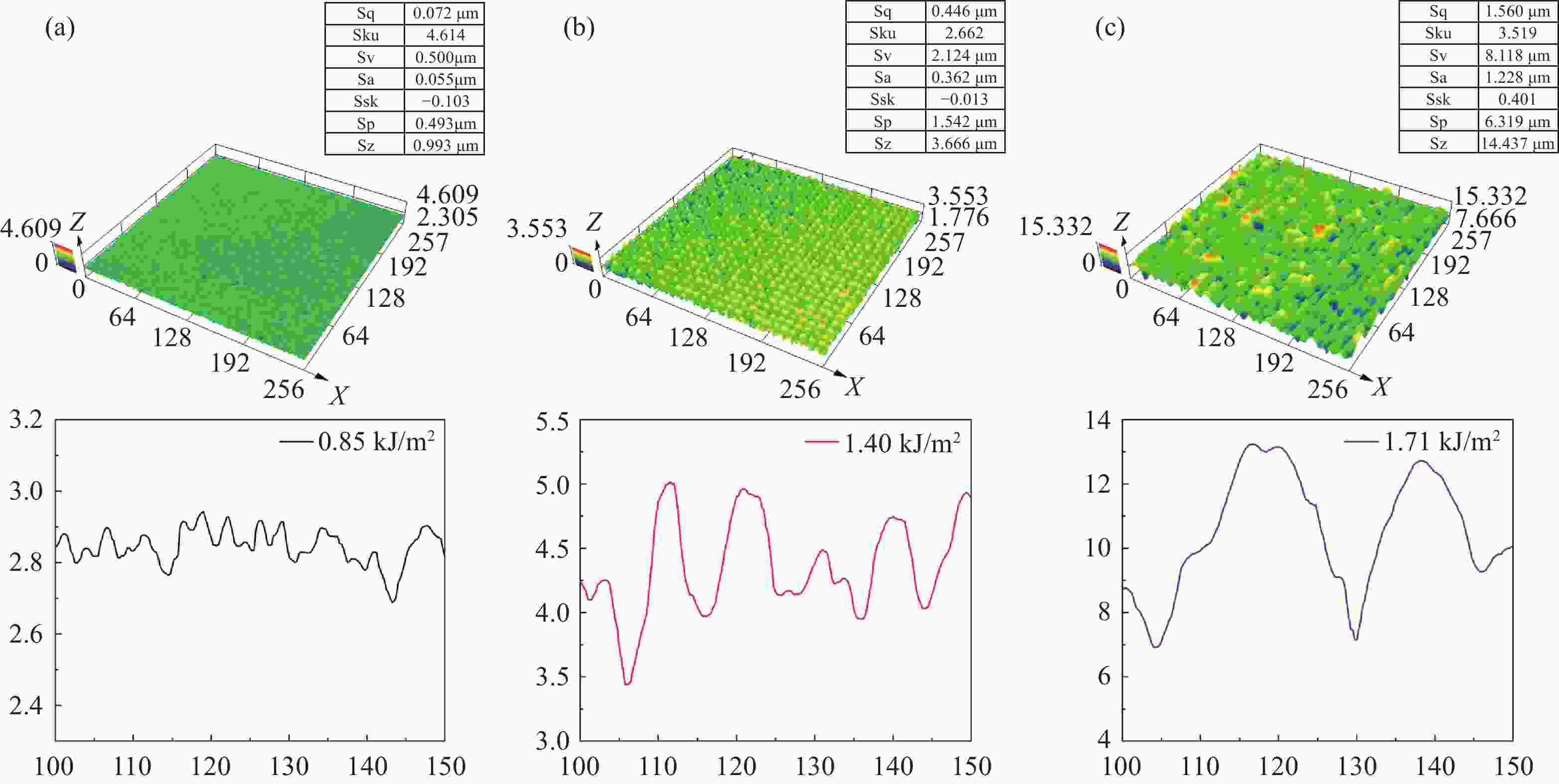
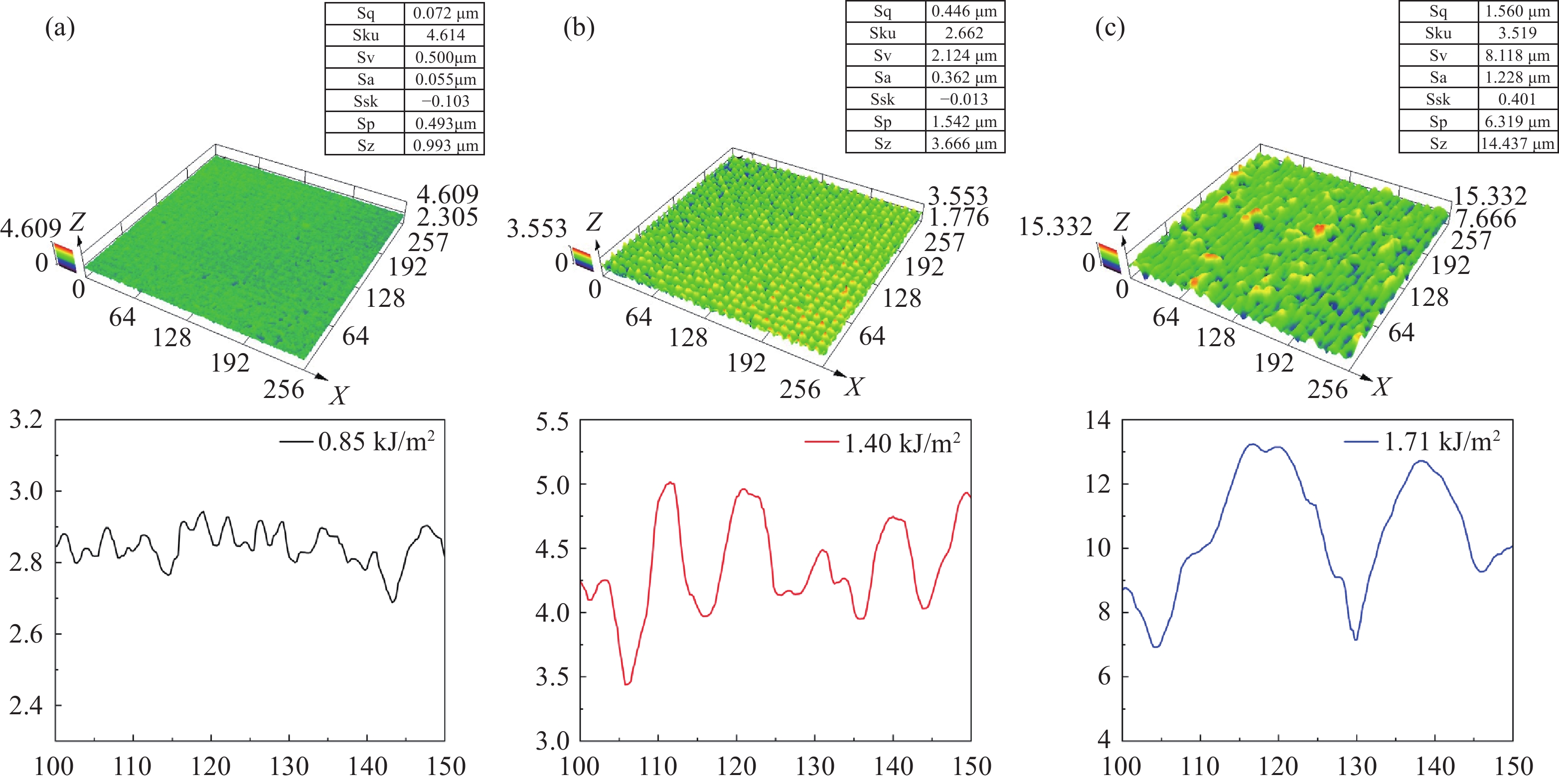
图 2 不同激光能量密度下 Se 掺杂硅样品的三维表面形貌及粗糙度测试结果:(a) 0.85 kJ/m2;(b) 1.40 kJ/m2;(c) 1.71 kJ/m2
Figure 2. Three-dimensional surface morphology and roughness measurement results of Se-doped silicon samples under different laser energy densities: (a) 0.85 kJ/m2; (b) 1.40 kJ/m2; (c) 1.71 kJ/m2.
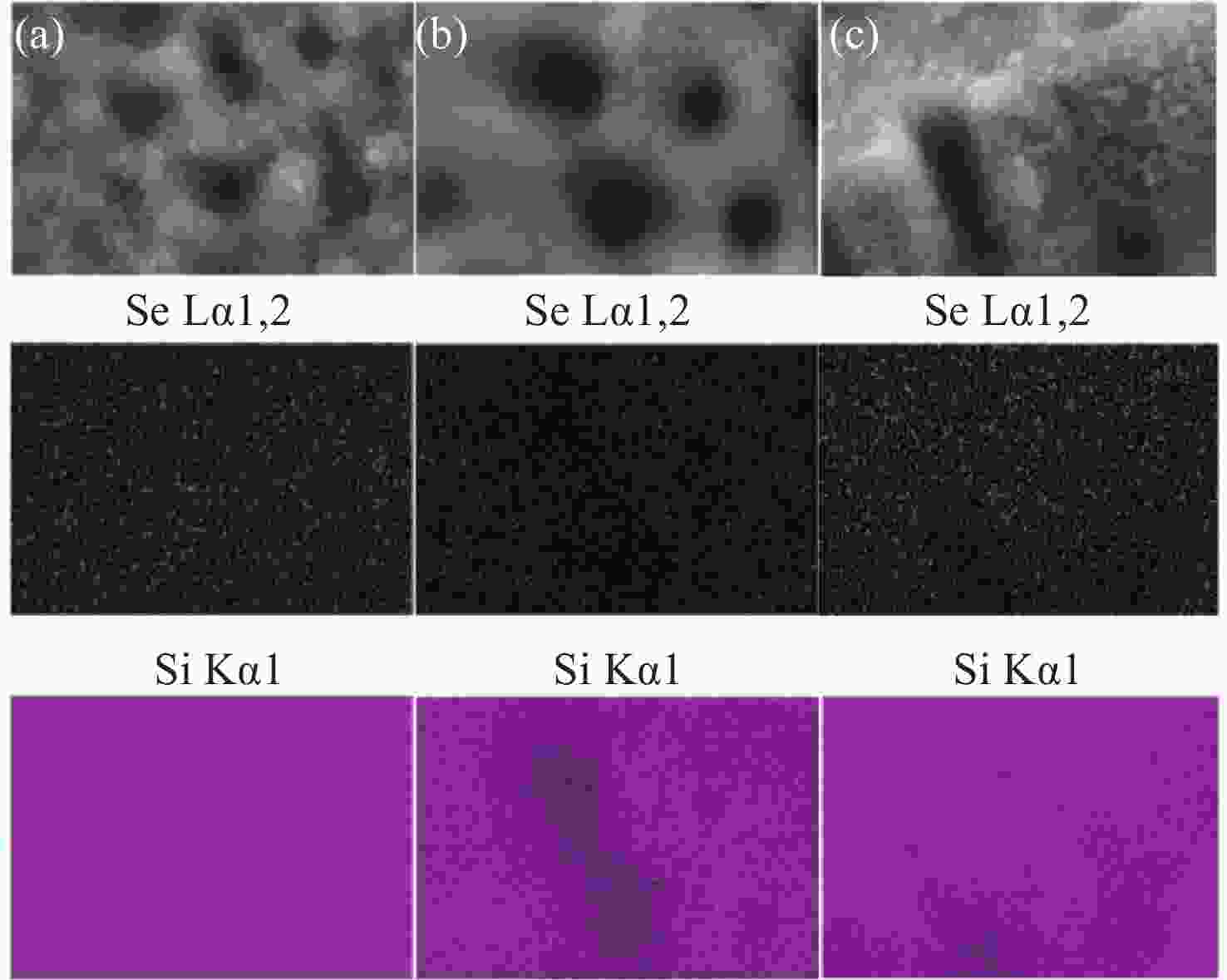
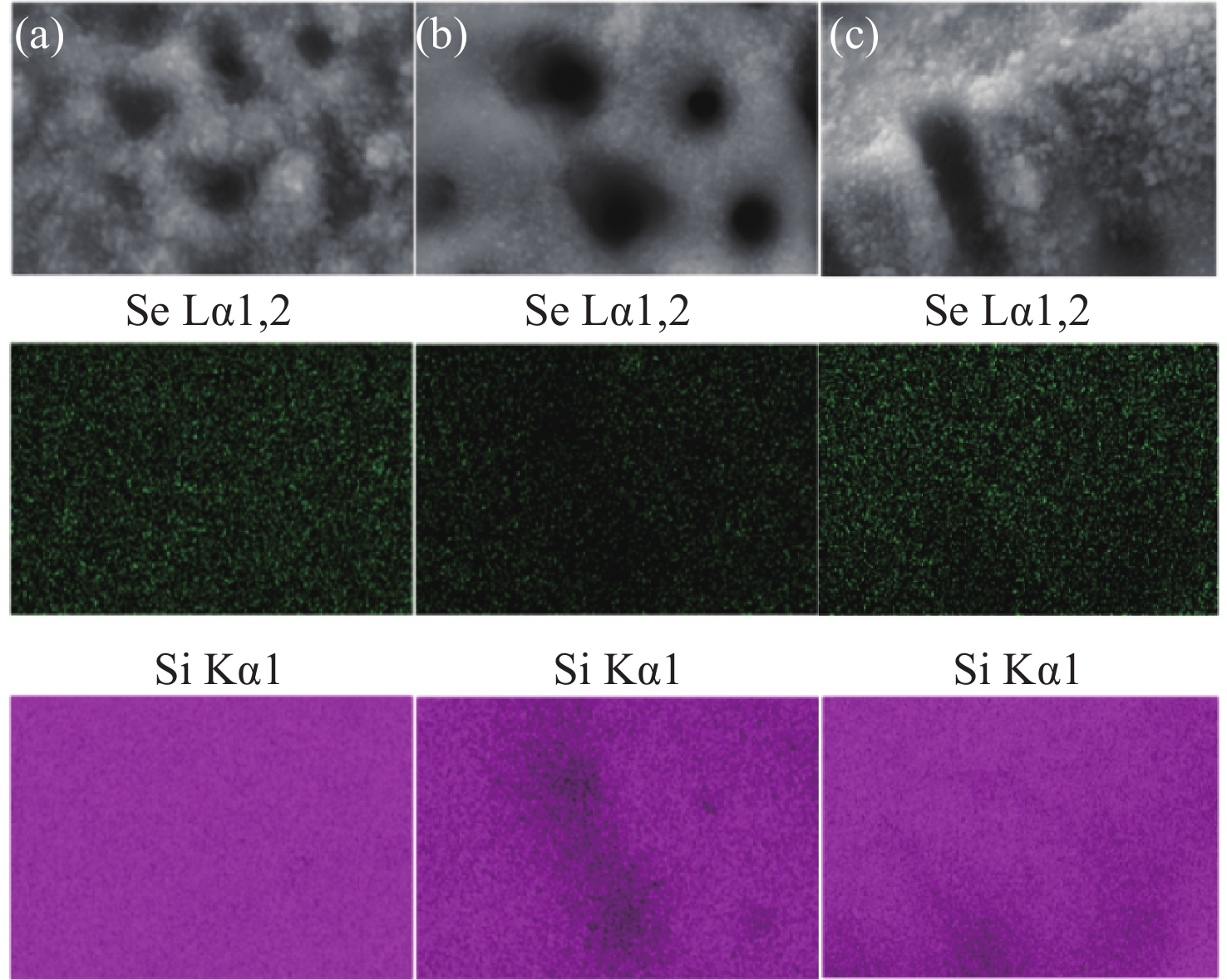
图 3 不同能量密度样品Se和硅的EDS能谱图(a)激光能量密度为0.85 kJ/m2;(b)激光能量密度为1.4 kJ/m2;(c)激光能量密度为1.71 kJ/m2
Figure 3. EDS spectra of Se and Si in samples with different energy densities: (a) laser scanning energy of 0.85 kJ/m2; (b) laser scanning energy of 1.4 kJ/m2; (c) laser scanning energy of 1.71 kJ/m2
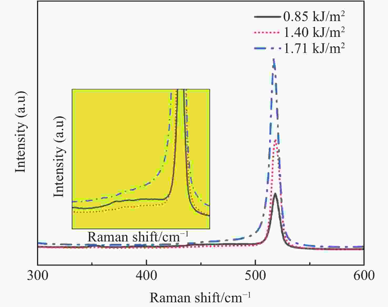
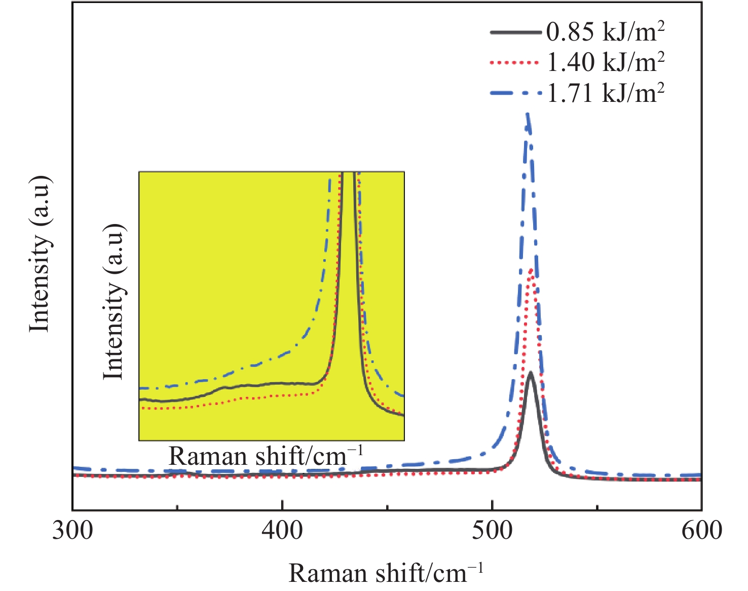
图 4 不同能量密度Se掺杂样品的拉曼光谱
Figure 4. Raman spectra of Se-doped samples at different energy densities
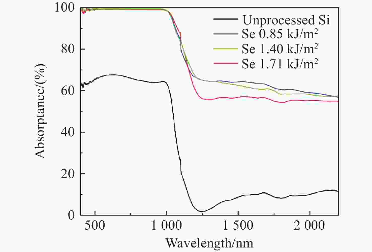
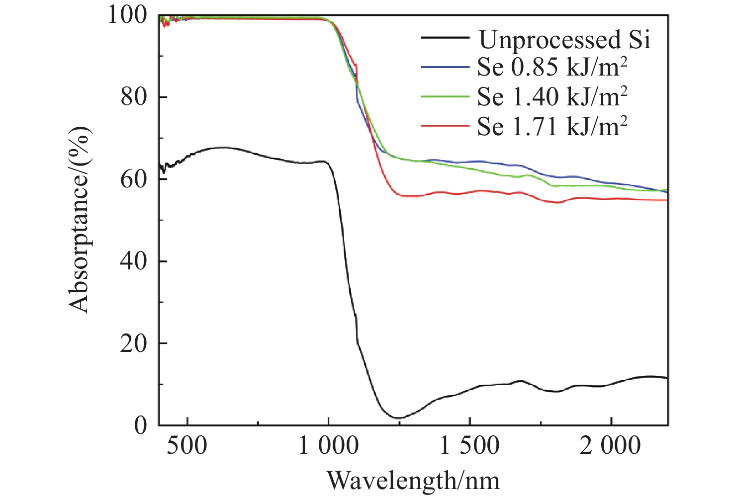
图 5 不同能量密度掺Se样品的吸收光谱
Figure 5. Absorption spectra of Se-doped samples at different energy densities
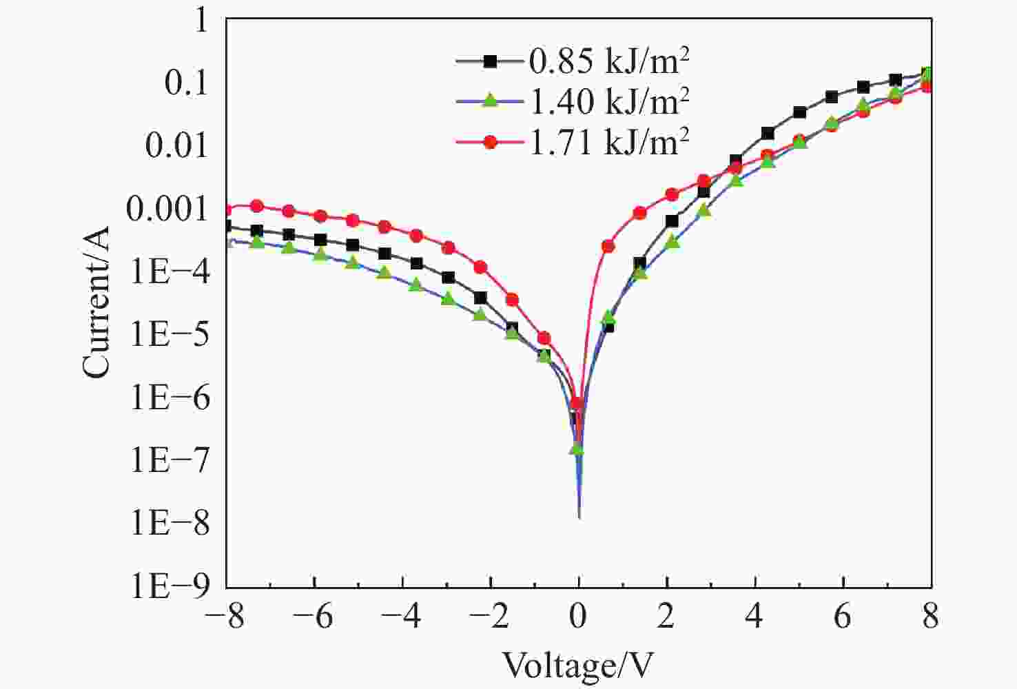
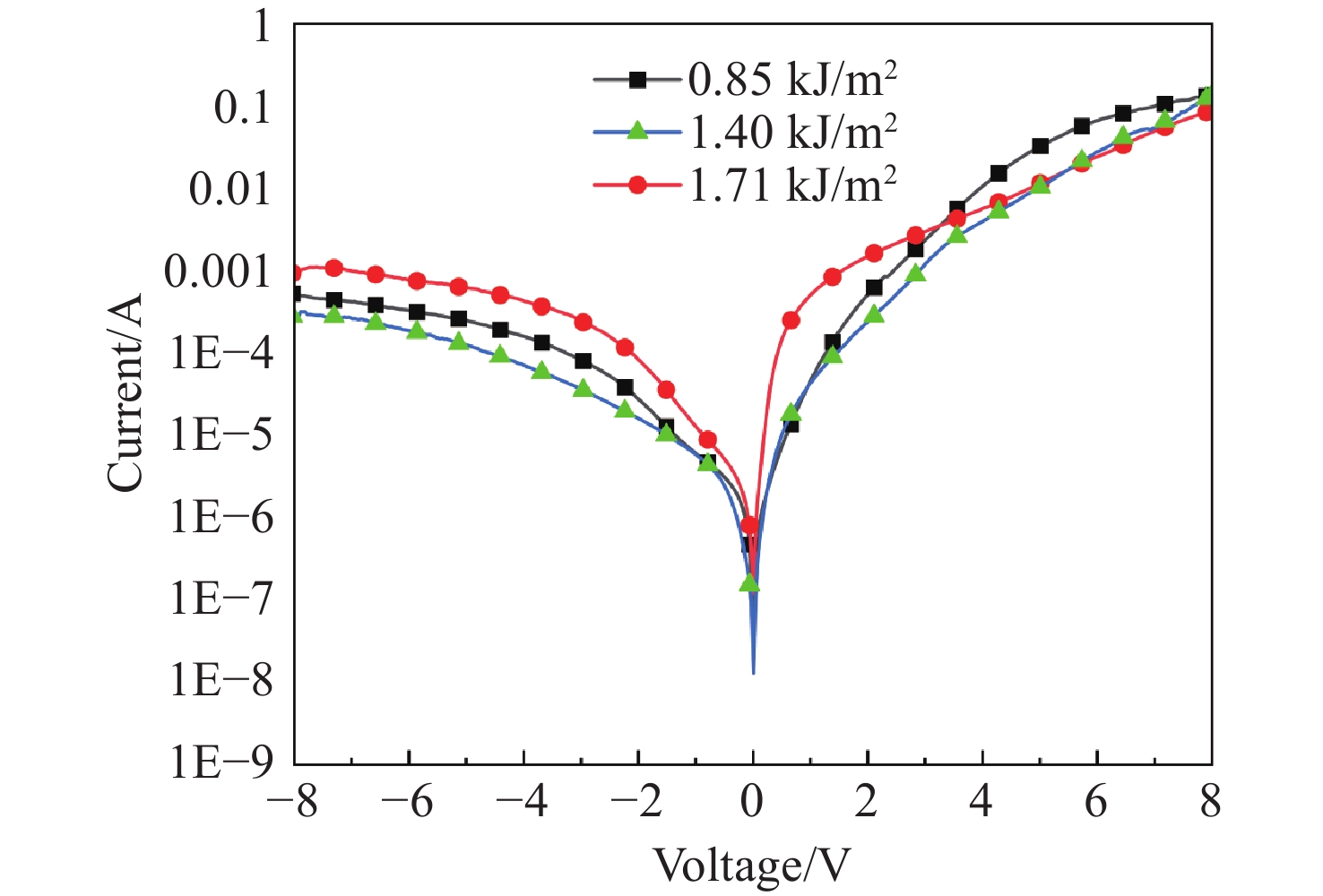
图 6 退火温度为500 °C的情况下不同能量密度制备的N+−N光电二极管在黑暗环境下的半对数I-V曲线
Figure 6. Semi-logarithmic I–V curves of N+−N photodiodes prepared at different energy densities with annealing temperature of 500 °C in dark condition
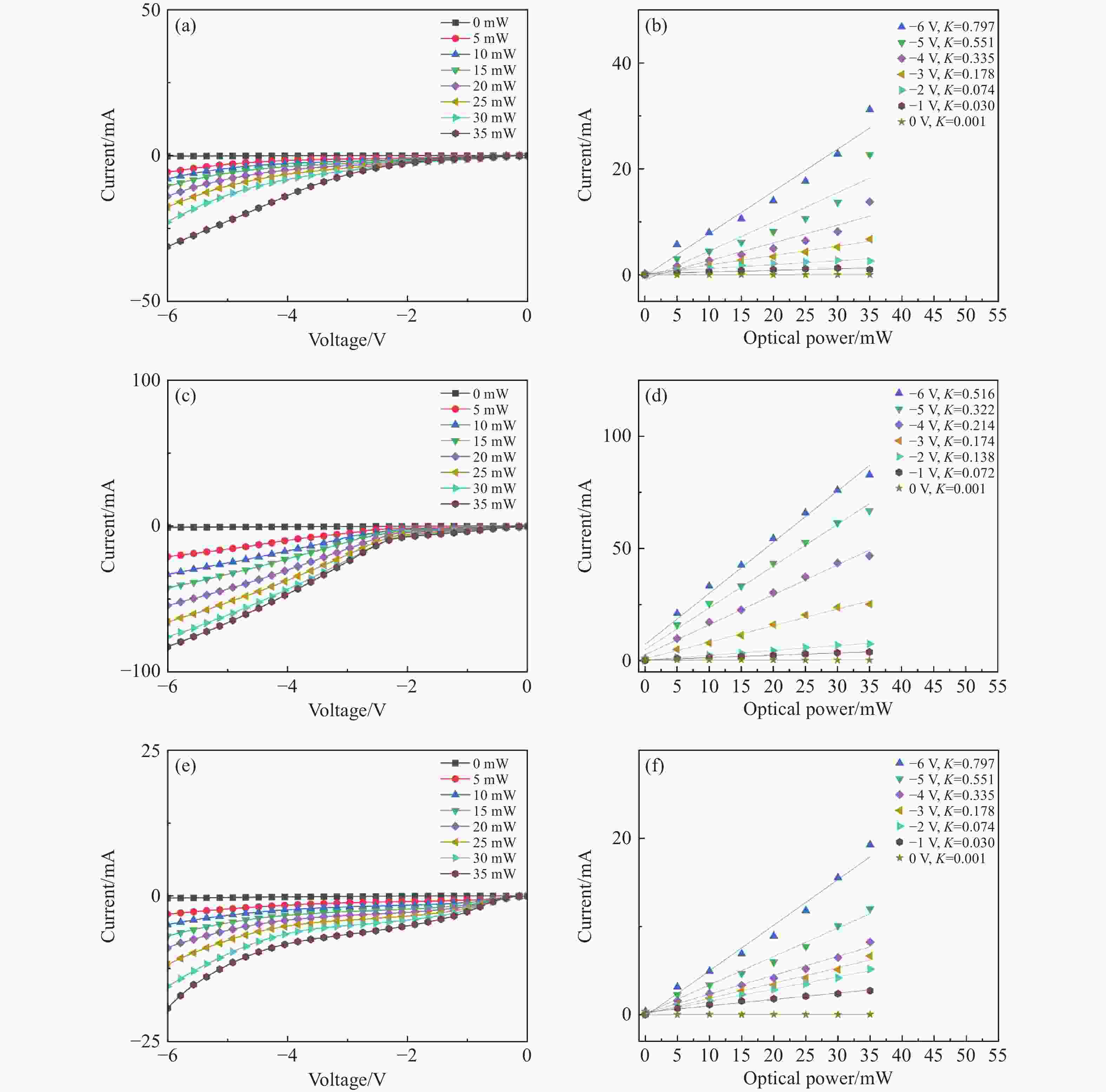
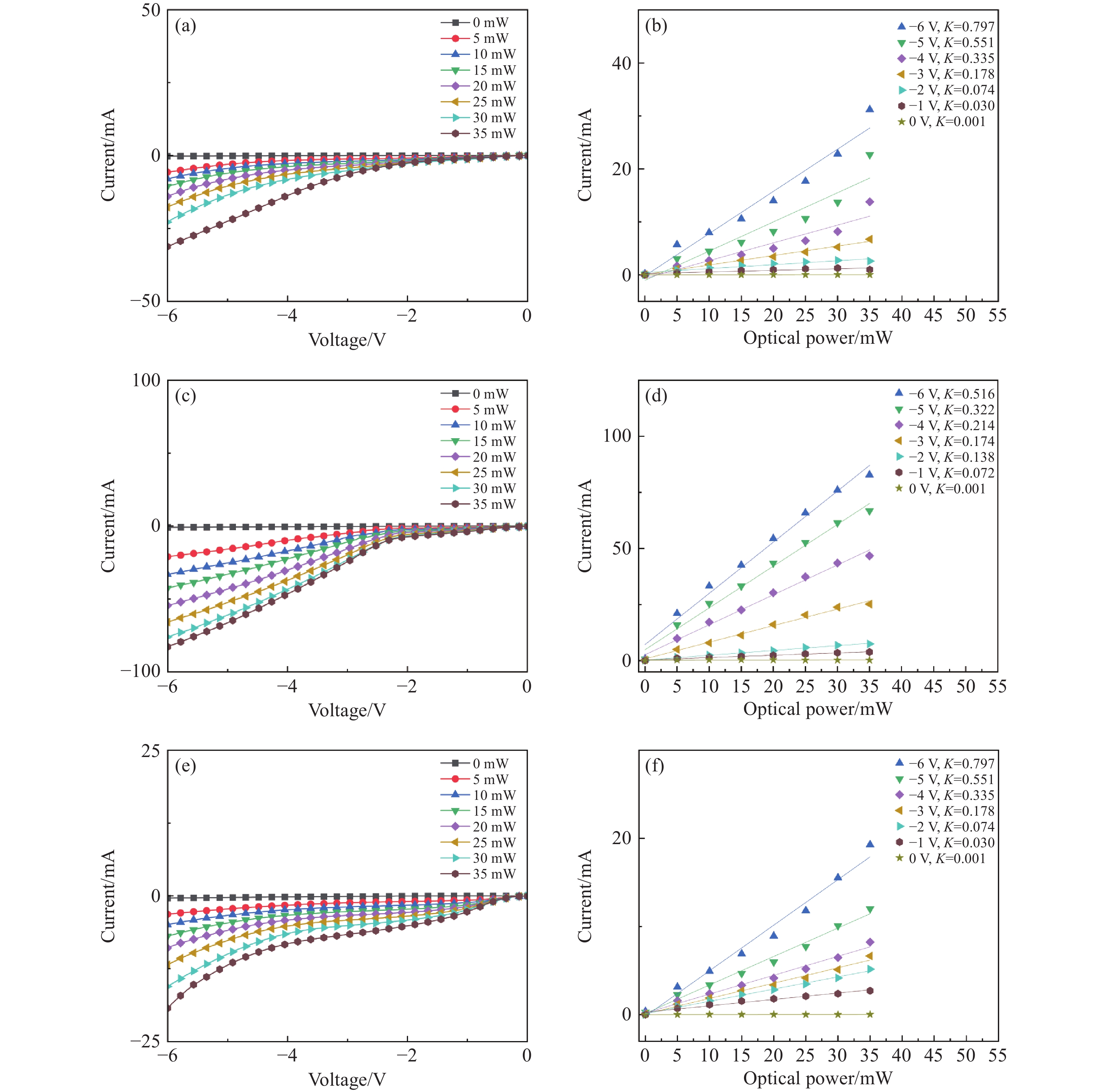
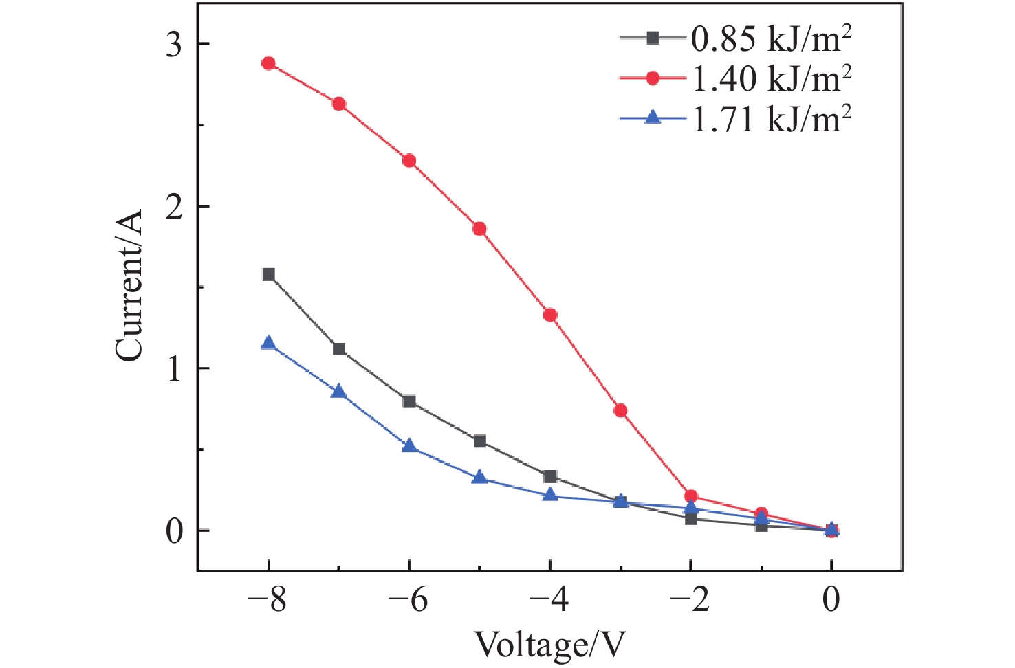
图 7 不同能量密度所制备光电二极管的光电流-电压曲线(左)和不同偏压下光电流与入射光功率关系(右)(a)(b)激光能量密度为0.85 kJ/m2;(c)(d)激光能量密度为1.40 kJ/m2;(e)(f)激光能量密度为1.71 kJ/m2
Figure 7. Photocurrent-voltage curves of photodiodes fabricated at different energy densities (left) and relationship between photocurrent and incident light power under different bias voltages (right): (a)(b) laser scanning energy of 0.85 kJ/m2; (c)(d) laser scanning energy of 1.40 kJ/m2; (e)(f) laser scanning energy of 1.71 kJ/m2
-
[1] LV J, ZHANG T, ZHANG P, et al. Review application of nanostructured black silicon[J]. Nanoscale Research Letters, 2018, 13(1): 110. doi: 10.1186/s11671-018-2523-4 [2] TONG ZH Y, BU M X, ZHANG Y Q, et al. Hyperdoped silicon: processing, properties, and devices[J]. Journal of Semiconductors, 2022, 43(9): 093101. doi: 10.1088/1674-4926/43/9/093101 [3] LI D D, KONG L H, FENG L P, et al. Large-area, high-resolution, flexible x-ray scintillator film based on a novel 0d hybrid cuprous halide[J]. Light: Advanced Manufacturing, 2025, 6(4): 44. doi: 10.37188/lam.2025.044 [4] GAO D, CHEN B J, SHA X ZH, et al. Near infrared emissions from both high efficient quantum cutting (173%) and nearly-pure-color upconversion in NaY(WO4)2: Er3+/Yb3+ with thermal management capability for silicon-based solar cells[J]. Light: Science & Applications, 2024, 13(1): 17. [5] LONG J B, WANG ZH K, PENG H F, et al. A chip-based optoelectronic-oscillator frequency comb[J]. eLight, 2025, 5(1): 14. doi: 10.1186/s43593-025-00094-w [6] WANG H, CHEN L, WU Y, et al. Advancing inorganic electro-optical materials for 5 G communications: from fundamental mechanisms to future perspectives[J]. Light: Science & Applications, 2025, 14(1): 190. [7] GREEN M A. Silicon Solar Cells: Advanced Principles & Practice[M]. Kensington: Centre for Photovoltaic Devices and Systems, University of New South Wales, 1995. [8] SZE S M, LI Y M, NG K K. Physics of Semiconductor Devices[M]. 4th ed. Hoboken: John Wiley & Sons, 2021. [9] LIU X G, COXON P R, PETERS M, et al. Black silicon: fabrication methods, properties and solar energy applications[J]. Energy & Environmental Science, 2014, 7(10): 3223-3263. doi: 10.1039/C4EE01152J [10] FAN ZH, CUI D F, ZHANG Z X, et al. Recent progress of black silicon: from fabrications to applications[J]. Nanomaterials, 2021, 11(1): 41. doi: 10.3390/nano11010041 [11] SUGIOKA K, CHENG Y. Ultrafast lasers-reliable tools for advanced materials processing[J]. Light: Science & Applications, 2014, 3(4): e149. [12] PHILLIPS K C, GANDHI H H, MAZUR E, et al. Ultrafast laser processing of materials: a review[J]. Advances in Optics and Photonics, 2015, 7(4): 684-712. doi: 10.1364/AOP.7.000684 [13] ZHAO ZH CH, KRAVTSOV V, WANG Z R, et al. Applications of ultrafast nano-spectroscopy and nano-imaging with tip-based microscopy[J]. eLight, 2025, 5(1): 1. doi: 10.1186/s43593-024-00079-1 [14] ZHAO J H, LI X B, CHEN Q D, et al. Ultrafast laser-induced black silicon, from micro-nanostructuring, infrared absorption mechanism, to high performance detecting devices[J]. Materials Today Nano, 2020, 11: 100078. doi: 10.1016/j.mtnano.2020.100078 [15] LI CH, ZHAO J H, CHEN ZH G. Infrared absorption and sub-bandgap photo-response of hyperdoped silicon by ion implantation and ultrafast laser melting[J]. Journal of Alloys and Compounds, 2021, 883: 160765. doi: 10.1016/j.jallcom.2021.160765 [16] FU J W, YANG D R, YU X G. Hyperdoped crystalline silicon for infrared photodetectors by pulsed laser melting: a review[J]. Physica Status Solidi (a), 2022, 219(14): 2100772. doi: 10.1002/pssa.202100772 [17] HUANG S, JIN X R, WU Q, et al. Ultrafast laser hyperdoped black silicon and its application in photodetectors: a review[J]. Physica Status Solidi (a), 2024, 221(24): 2400127. doi: 10.1002/pssa.202400127 [18] UMEZU I, WARRENDER J M, CHARNVANICHBORIKARN S, et al. Emergence of very broad infrared absorption band by hyperdoping of silicon with chalcogens[J]. Journal of Applied Physics, 2013, 113(21): 213501. doi: 10.1063/1.4804935 [19] HER T H, FINLAY R J, WU C, et al. Microstructuring of silicon with femtosecond laser pulses[J]. Applied Physics Letters, 1998, 73(12): 1673-1675. doi: 10.1063/1.122241 [20] SHEEHY M A, TULL B R, FRIEND C M, et al. Chalcogen doping of silicon via intense femtosecond-laser irradiation[J]. Materials Science and Engineering: B, 2007, 137(1-3): 289-294. doi: 10.1016/j.mseb.2006.10.002 [21] HU SH X, HAN P D, WANG SH, et al. Improved photoresponse characteristics in Se-doped Si photodiodes fabricated using picosecond pulsed laser mixing[J]. Semiconductor Science and Technology, 2012, 27(10): 102002. doi: 10.1088/0268-1242/27/10/102002 [22] DU L Y, YIN J, ZENG W, et al. Fabrication of micro-nano structure Se-doped silicon via picosecond laser irradiation assisted by dopant film[J]. Materials Letters, 2023, 331: 133463. doi: 10.1016/j.matlet.2022.133463 [23] GUO H, XIE J W, HE G ZH, et al. A review of ultrafast laser micro/nano fabrication: material processing, surface/interface controlling, and devices fabrication[J]. Nano Research, 2024, 17(7): 6212-6230. doi: 10.1007/s12274-024-6644-z [24] GROSS J M, SHAVANDI S R, ZAGORAC T, et al. Picosecond versus femtosecond-laser ablation of silicon in atmosphere[J]. Journal of Laser Applications, 2023, 35(4): 042053. doi: 10.2351/7.0001206 [25] HAMAD A H. Effects of different laser pulse regimes (nanosecond, picosecond and femtosecond) on the ablation of materials for production of nanoparticles in liquid solution[M]//VISKUP R. High Energy and Short Pulse Lasers. Rijeka: InTech, 2016. [26] ZHOU SH Q, LIU F, PRUCNAL S, et al. Hyperdoping silicon with selenium: solid vs. liquid phase epitaxy[J]. Scientific Reports, 2015, 5(1): 8329. doi: 10.1038/srep08329 [27] WANG M, DEBERNARDI A, ZHANG W X, et al. Critical behavior of the insulator-to-metal transition in Te-hyperdoped Si[J]. Physical Review B, 2020, 102(8): 085204. doi: 10.1103/PhysRevB.102.085204 [28] DU L Y, LIU SH P, CHEN F S, et al. Effects of dopant film thickness on near-infrared photodiode response based on Se-doped silicon fabricated by picosecond laser[J]. Infrared Physics & Technology, 2025, 150: 105933. doi: 10.1016/j.infrared.2025.105933 [29] ATTEIA F, LE ROUZO J, DENAIX L, et al. Morphologies and optical properties of black silicon by room temperature reactive ion etching[J]. Materials Research Bulletin, 2020, 131: 110973. doi: 10.1016/j.materresbull.2020.110973 [30] ZHANG X M, LI W N, JIN CH, et al. Effects of black silicon surface morphology induced by a femtosecond laser on absorptance and photoelectric response efficiency[J]. Photonics, 2024, 11(10): 947. doi: 10.3390/photonics11100947 [31] KOMAROV F, PARKHOMENKO I, ALZHANOVA A, et al. Broad infrared absorption band through ion beam hyperdoping of silicon with selenium[J]. Applied Surface Science, 2023, 639: 158168. doi: 10.1016/j.apsusc.2023.158168 [32] LEDINSKÝ M, FEKETE L, STUCHLÍK J, et al. Characterization of mixed phase silicon by Raman spectroscopy[J]. Journal of Non-Crystalline Solids, 2006, 352(9-20): 1209-1212. doi: 10.1016/j.jnoncrysol.2005.10.072 [33] FANG Y J, ARMIN A, MEREDITH P, et al. Accurate characterization of next-generation thin-film photodetectors[J]. Nature Photonics, 2019, 13(1): 1-4. doi: 10.1038/s41566-018-0288-z -

 下载:
下载:


计量
- 文章访问数: 190
- HTML全文浏览量: 65
- PDF下载量: 15
- 被引次数: 0
