


Low-loss waveguide design for full visible spectrum on-chip photonic devices
doi: 10.37188/CO.EN-2025-0036
-
摘要:
将可见光集成光学器件的工作波段扩展至全可见光谱段具有重要意义,它可以增强微型光谱仪的检测精度与适用性、拓宽可见光通信的带宽、使生物传感器能够同时检测复杂样品中的多种生物分子等。波导是集成光学器件的核心基础元件,然而目前对全可见光波导的研究并不完善。本文提出了一种支持全可见光谱段(435−760 nm)的波导设计,使用数值仿真方法分析了不同波导结构的传输特性,发现波导内无法实现整个可见光谱的单模传输。在多模传输条件下,通过分析波导中传播损耗与模式分布,确定了可实现低损耗传输的最佳波导尺寸、弯曲半径与波导间距等参数。对于平板波导,厚度≥1 μm可确保偏振不敏感;对于厚度为1 μm的条形波导,宽度≥2 μm可显著降低由侧壁粗糙度引起的散射损耗;对于宽1 μm、厚2 μm的条形波导,弯曲半径≥10 μm,波导间距≥0.4 μm时,辐射损耗可以忽略,且光不会耦合到相邻波导。此外,评估了制备公差对波导性能的影响。与之前主要关注可见光谱内窄波段的研究不同,本工作中提出的设计能够在单个波导中传输全可见光谱,从而促进片上全可见光谱器件的带宽扩展和性能增强。
Abstract:Extending the operational wavelength range of integrated optical devices to cover the entire visible spectrum holds significant importance, as it can enhance the detection accuracy and applicability of miniaturized spectrometers, broaden the bandwidth of visible light communication, and enable biosensors to simultaneously detect multiple biomolecules in complex samples. As the fundamental building block of integrated optical devices, waveguides have not yet been thoroughly investigated for full visible spectrum operation. This work presents a waveguide design supporting the full visible spectrum (435−760 nm). Numerical simulations were employed to analyze the transmission characteristics of various waveguide structures, revealing that single-mode propagation cannot be achieved across the entire visible spectrum. Under multimode propagation conditions, key parameters such as propagation loss and mode distribution were systematically examined to determine the optimal waveguide dimensions, bending radii, and waveguide spacings for low-loss transmission. For slab waveguides, a thickness ≥1 μm ensures polarization insensitivity. For strip waveguides with a thickness of 1 μm, a width ≥2 μm significantly reduces scattering loss induced by sidewall roughness. For strip waveguides with a width of 1 μm and thickness of 2 μm, radiation loss becomes negligible when the bending radius ≥10 μm and waveguide spacing ≥0.4 μm, while maintaining effective isolation from adjacent waveguides. Additionally, the impact of fabrication tolerances on waveguide performance was evaluated. In contrast to previous studies primarily focusing on narrow spectral bands within the visible range, the proposed design enables full visible spectrum transmission in a single waveguide, thereby facilitating bandwidth expansion and performance enhancement for on-chip full visible spectrum devices.
-
Key words:
- integrated optics devices /
- waveguides /
- visible light /
- low-loss /
- silicon nitride
-
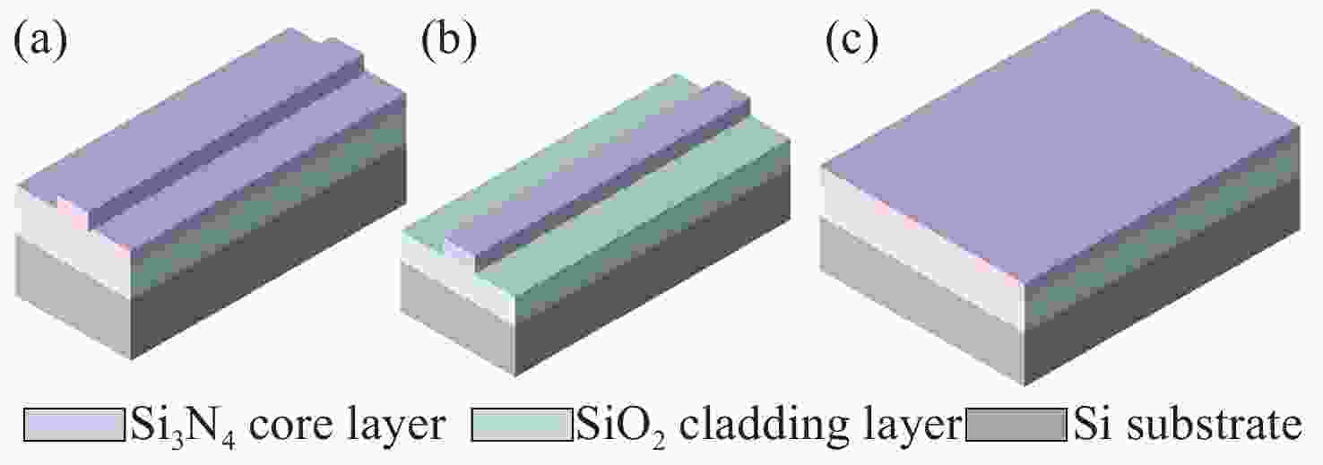
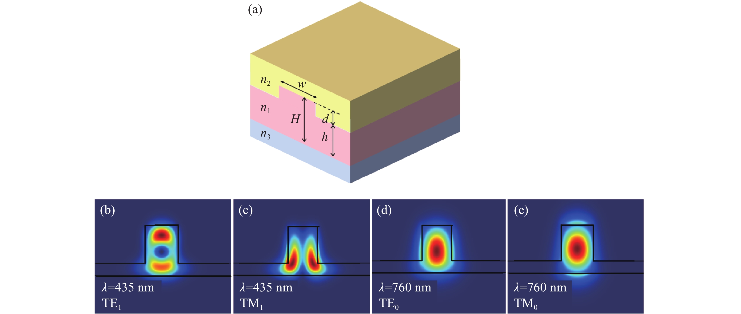
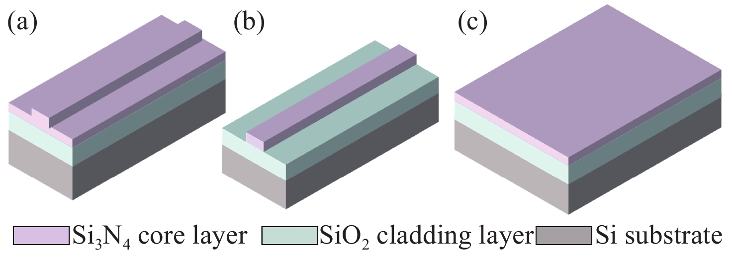
Figure 1. Schematic diagrams of (a) rib waveguide, (b) rectangular waveguide, and (c) slab waveguide
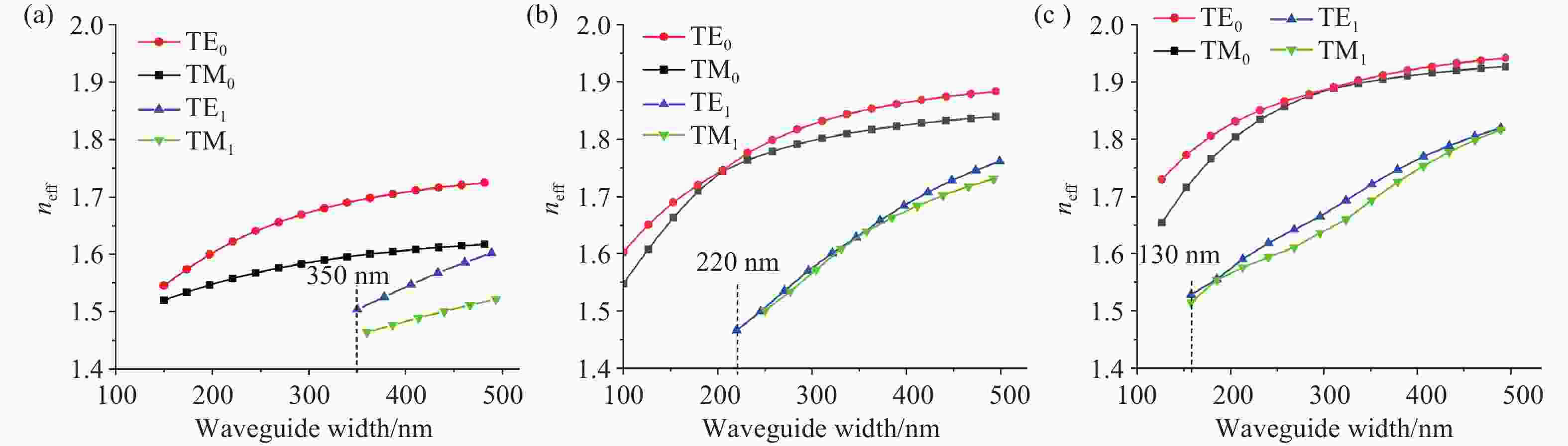
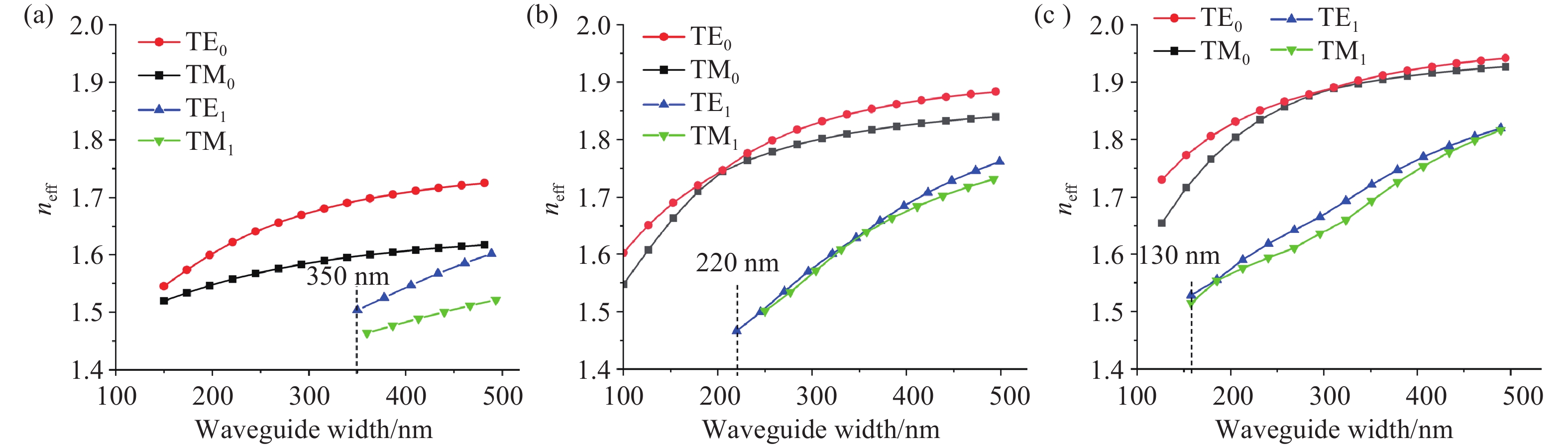
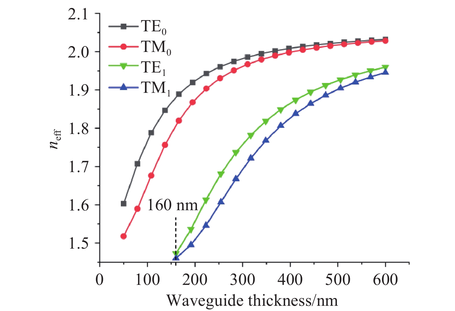
Figure 2. Effective refractive index as a function of waveguide width for the waveguide thicknesses of (a) 100 nm, (b) 200 nm, and (c) 300 nm
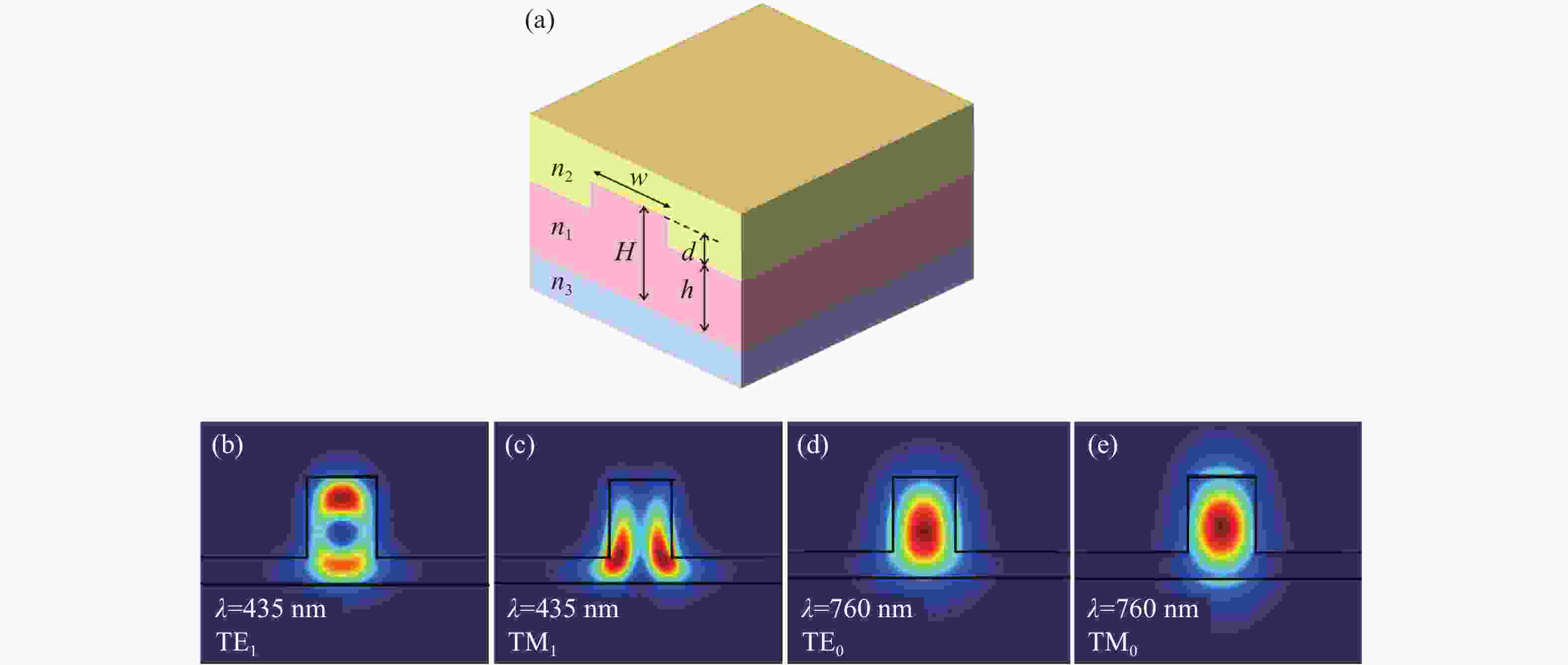
Figure 3. Mode distributions in the critically dimensioned rib waveguide. (a) TE1 and (b) TM1 at 435 nm, (c) TE0 and (d) TM0 at 760 nm
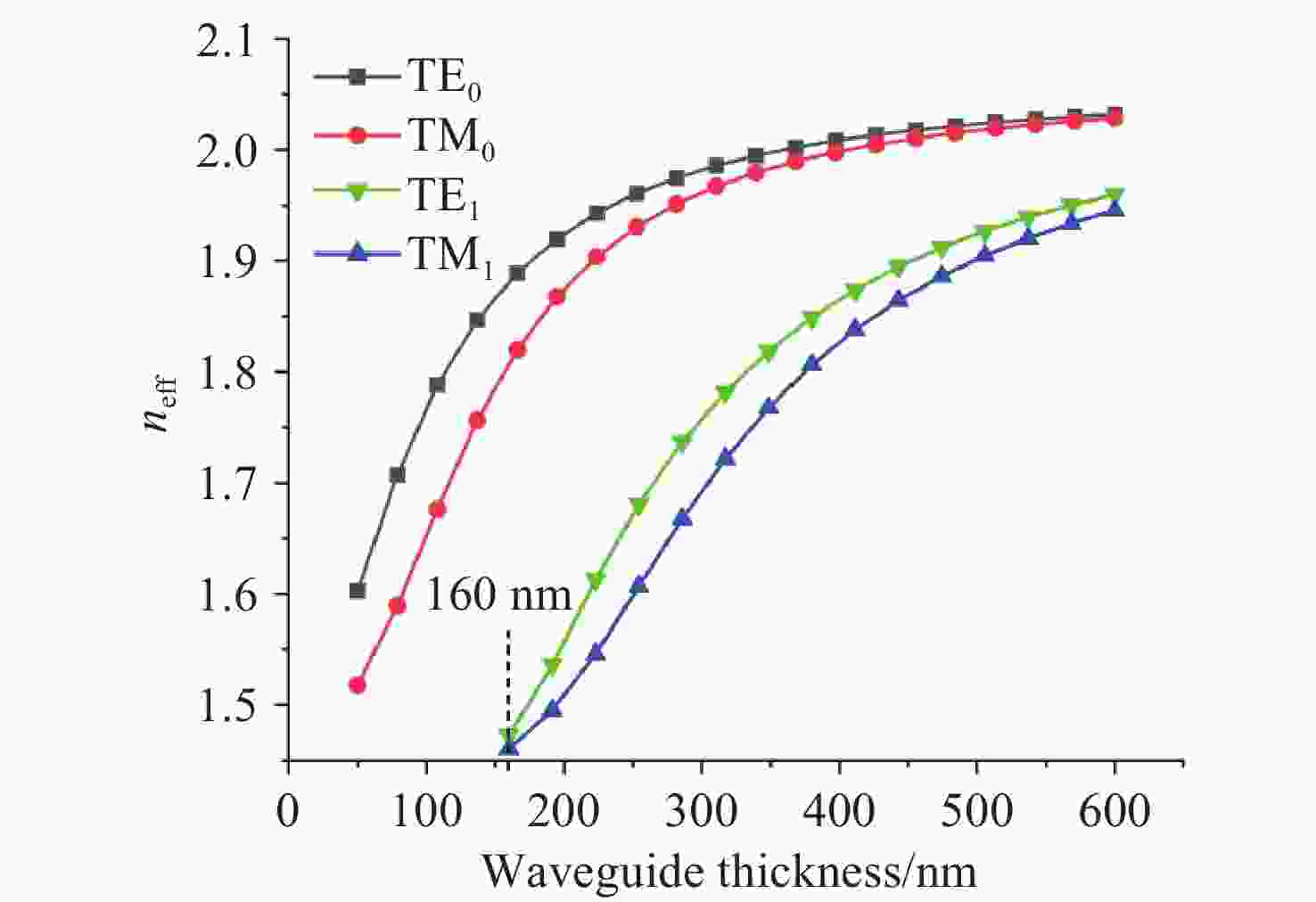
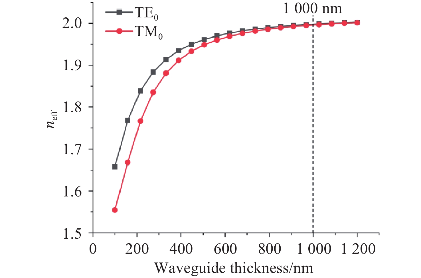
Figure 4. Variation of the effective refractive index with the thickness of the slab waveguide
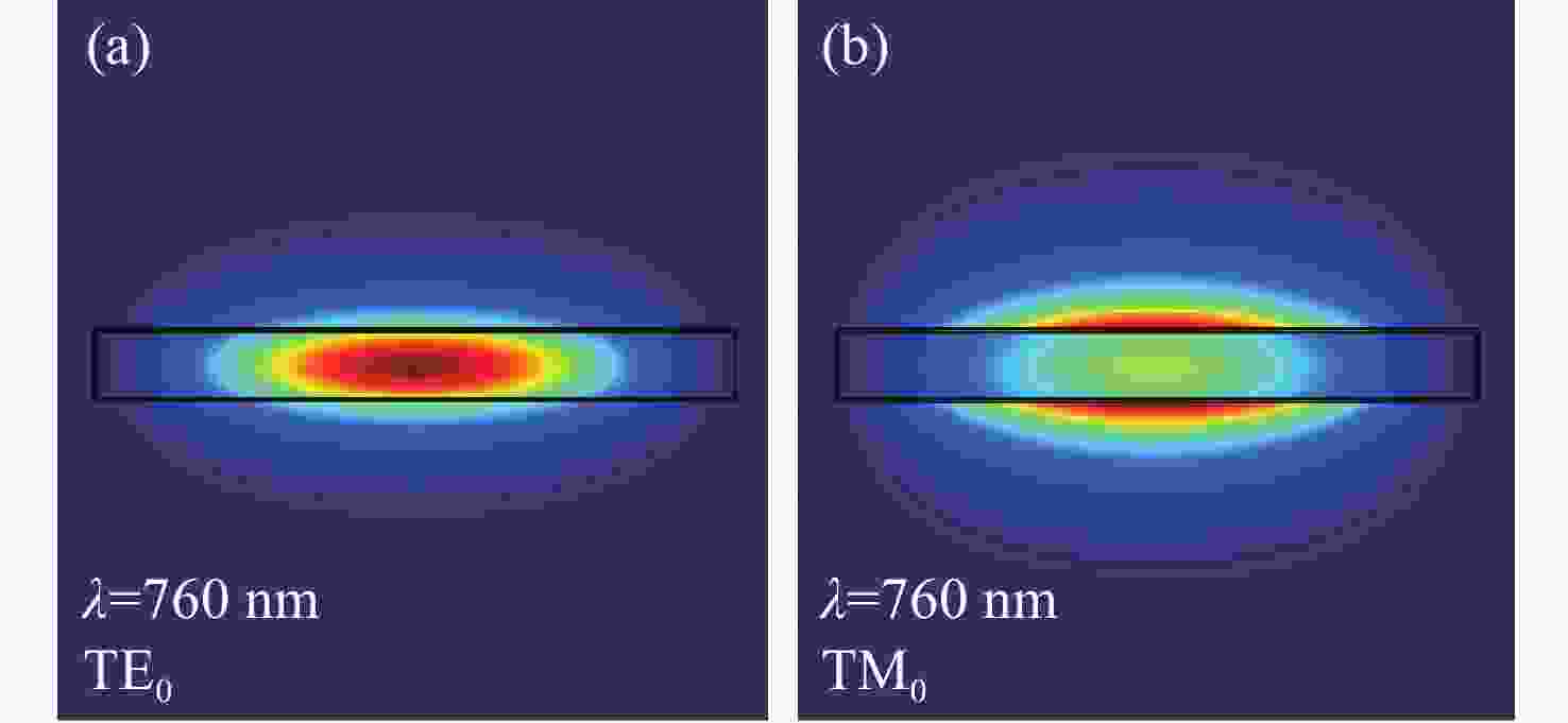
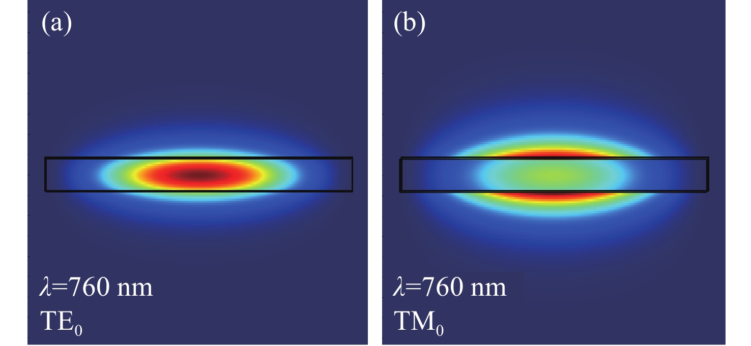
Figure 5. (a) TE0 and (b) TM0 mode distributions in the slab waveguide at 760 nm wavelength
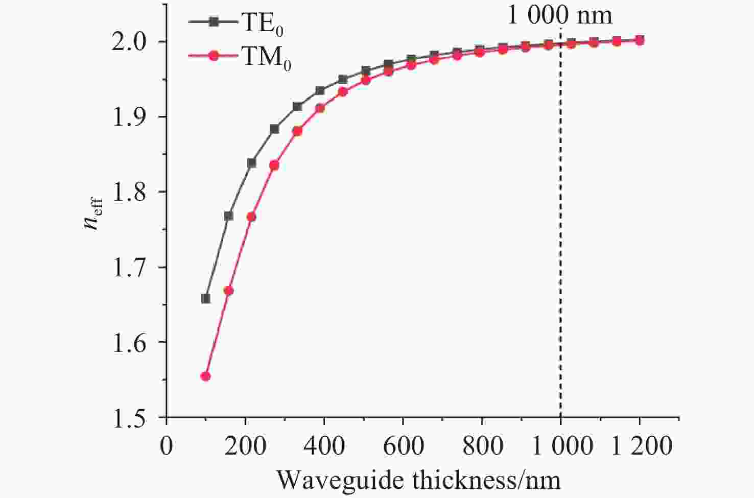
Figure 6. Effective refractive indices of TE0 and TM0 modes in a slab waveguide as a function of thickness at 597.5 nm wavelength
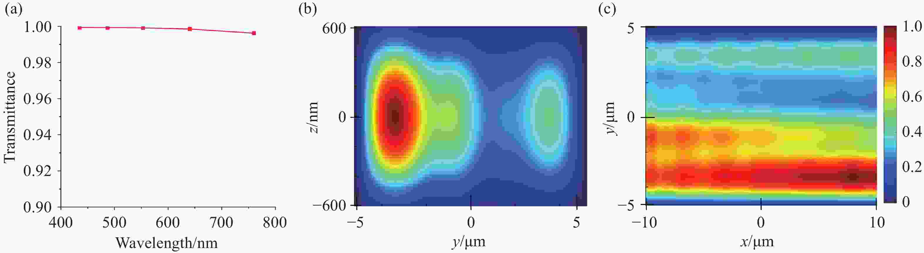
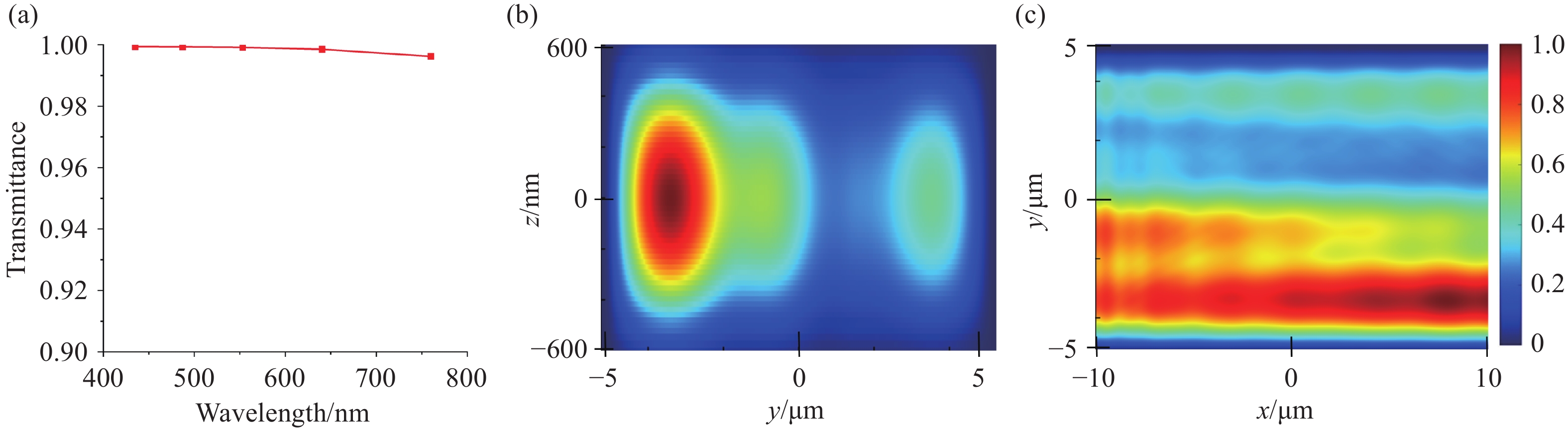
Figure 7. (a) Transmittance, (b) output electric field, and (c) electric field propagation in the slab waveguide

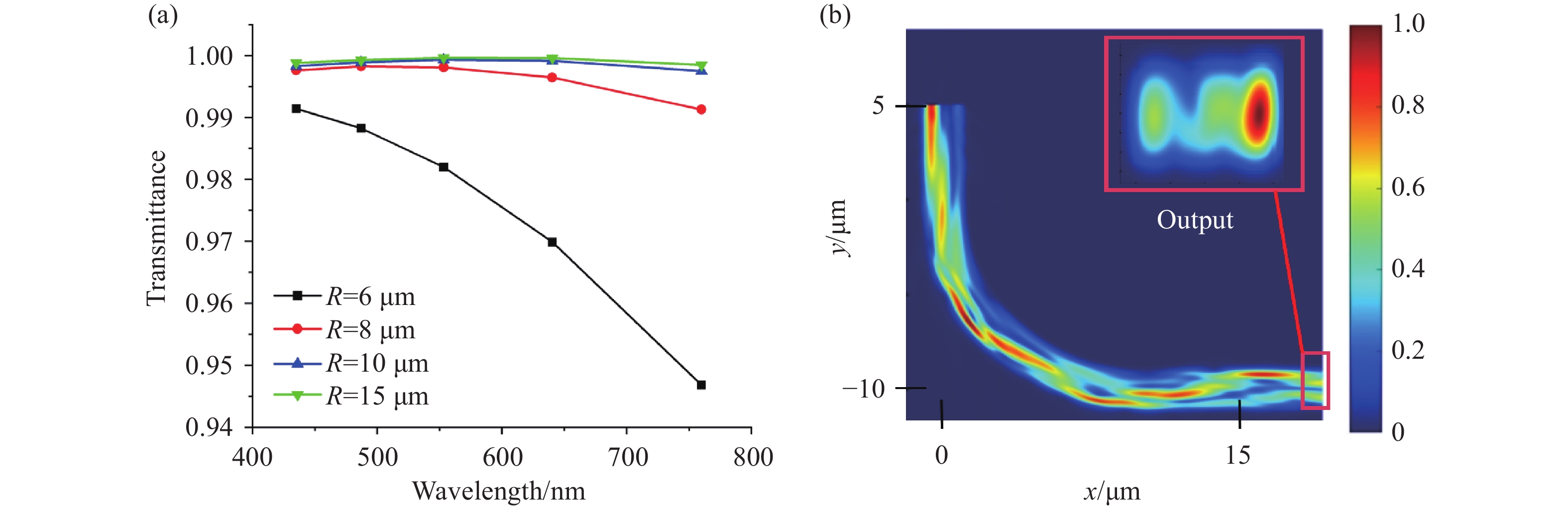
Figure 9. (a) Variation of the transmittance with the bending radius. (b) Electric field propagation at R=10 μm
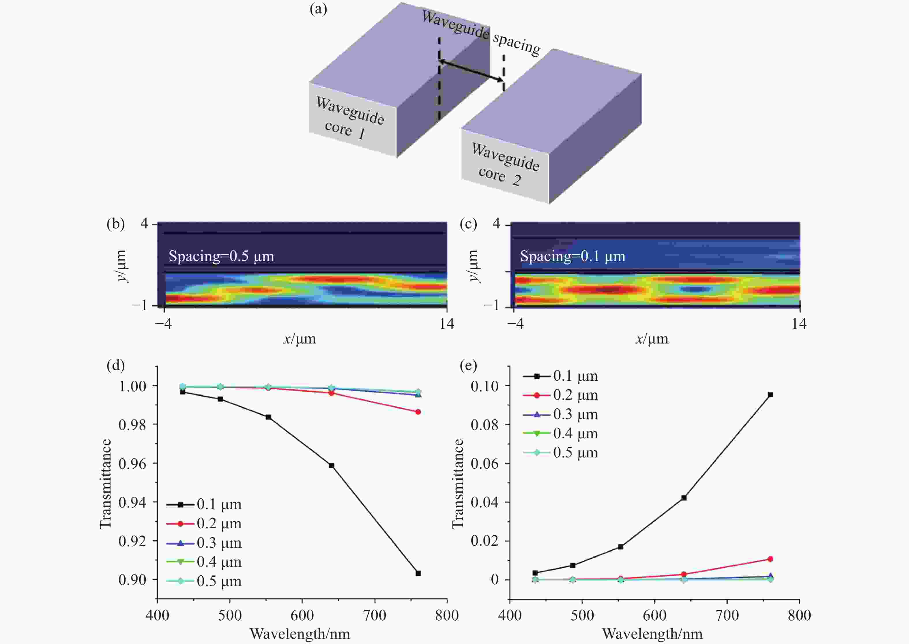
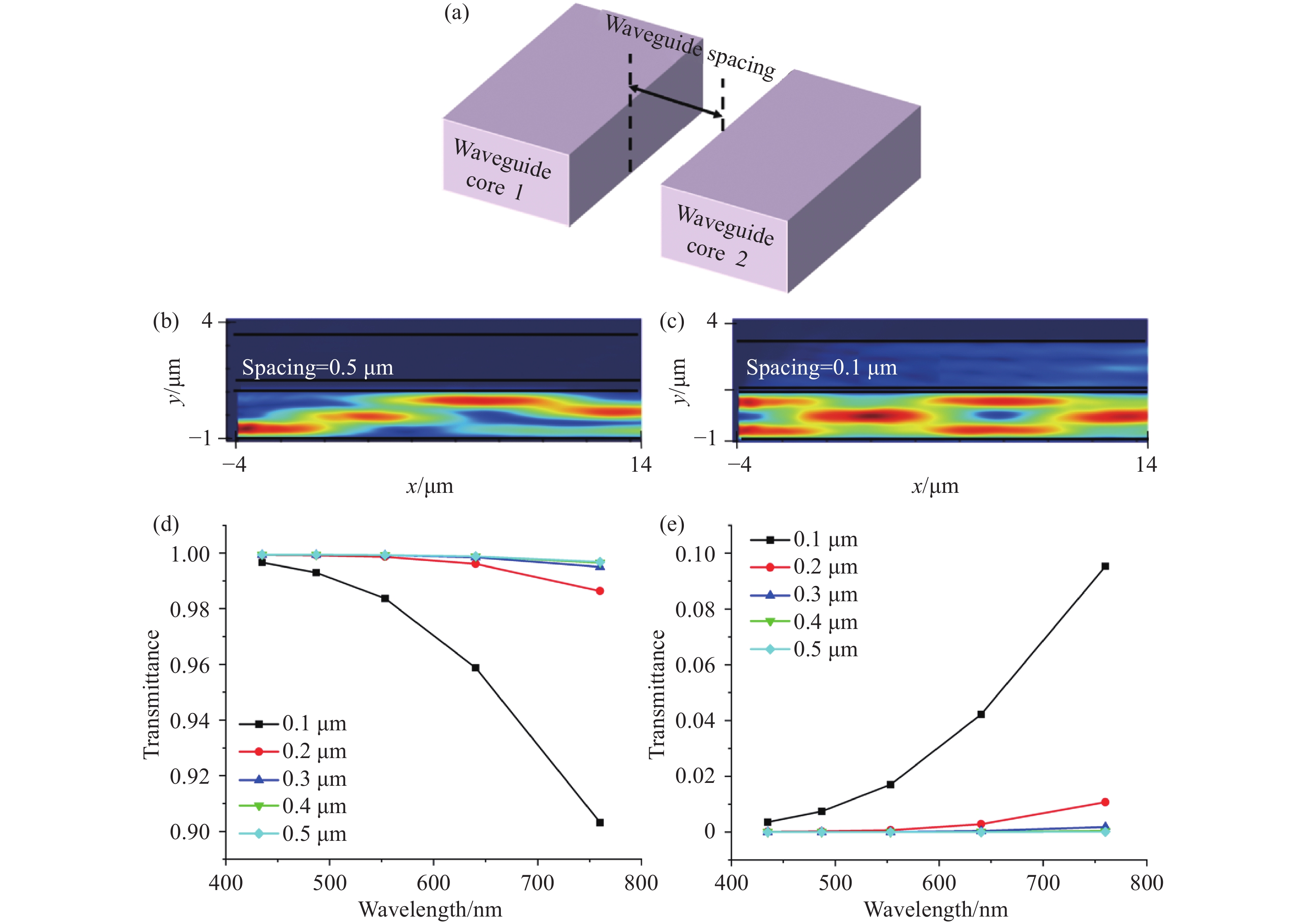
Figure 10. (a) Schematic diagram of the waveguide spacing. Electric field coupling at waveguide spacings of (b) 0.5 μm and (c) 0.1 μm. Transmittance of the (d) source waveguide and the (e) adjacent waveguide as a function of waveguide spacing
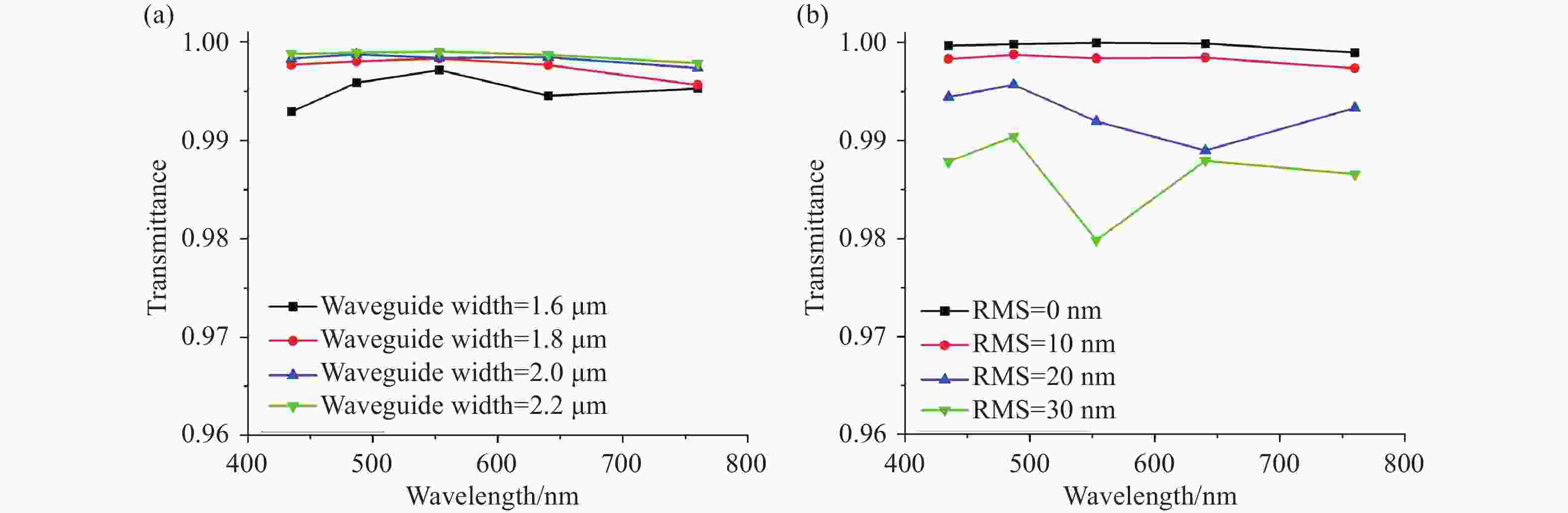
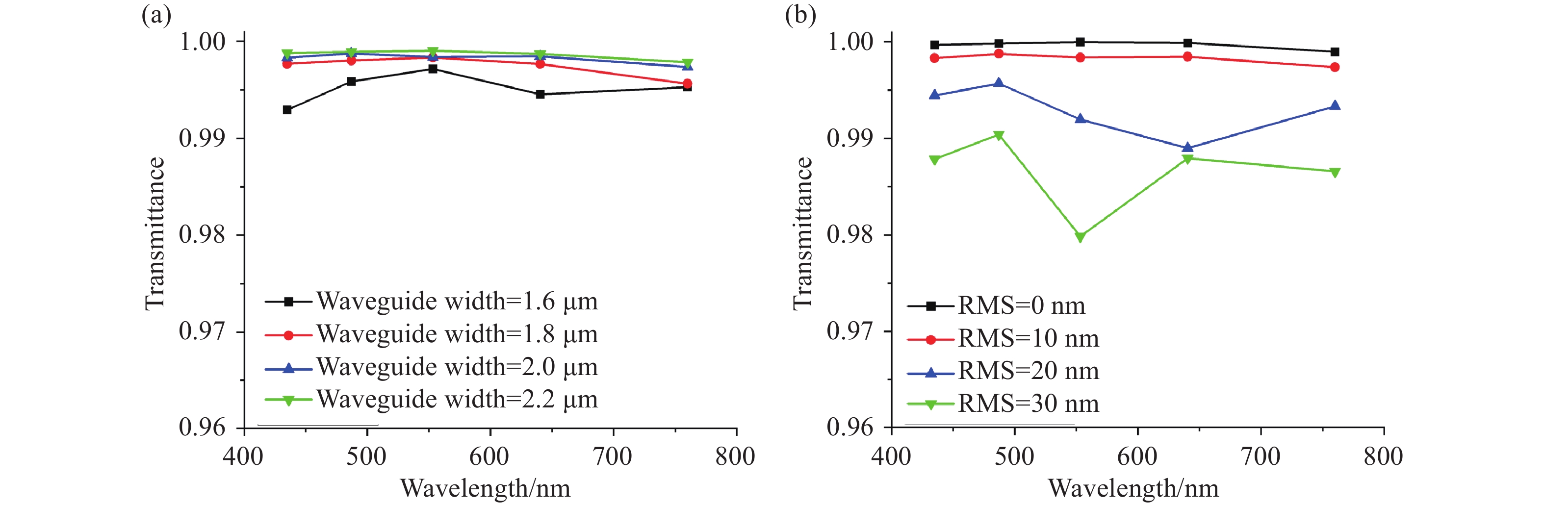
Figure 12. (a) Variation of transmittance with the width of the waveguide at RMS=10 nm. (b) Variation of transmittance with the sidewall roughness for a 2 μm wide waveguide
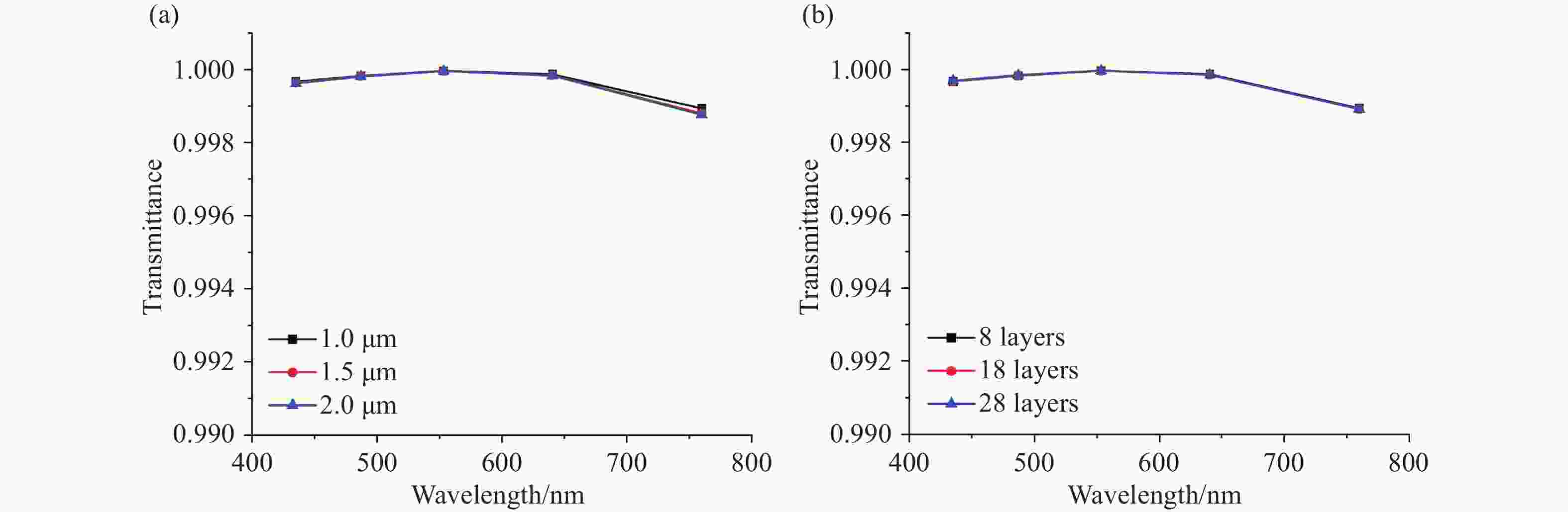
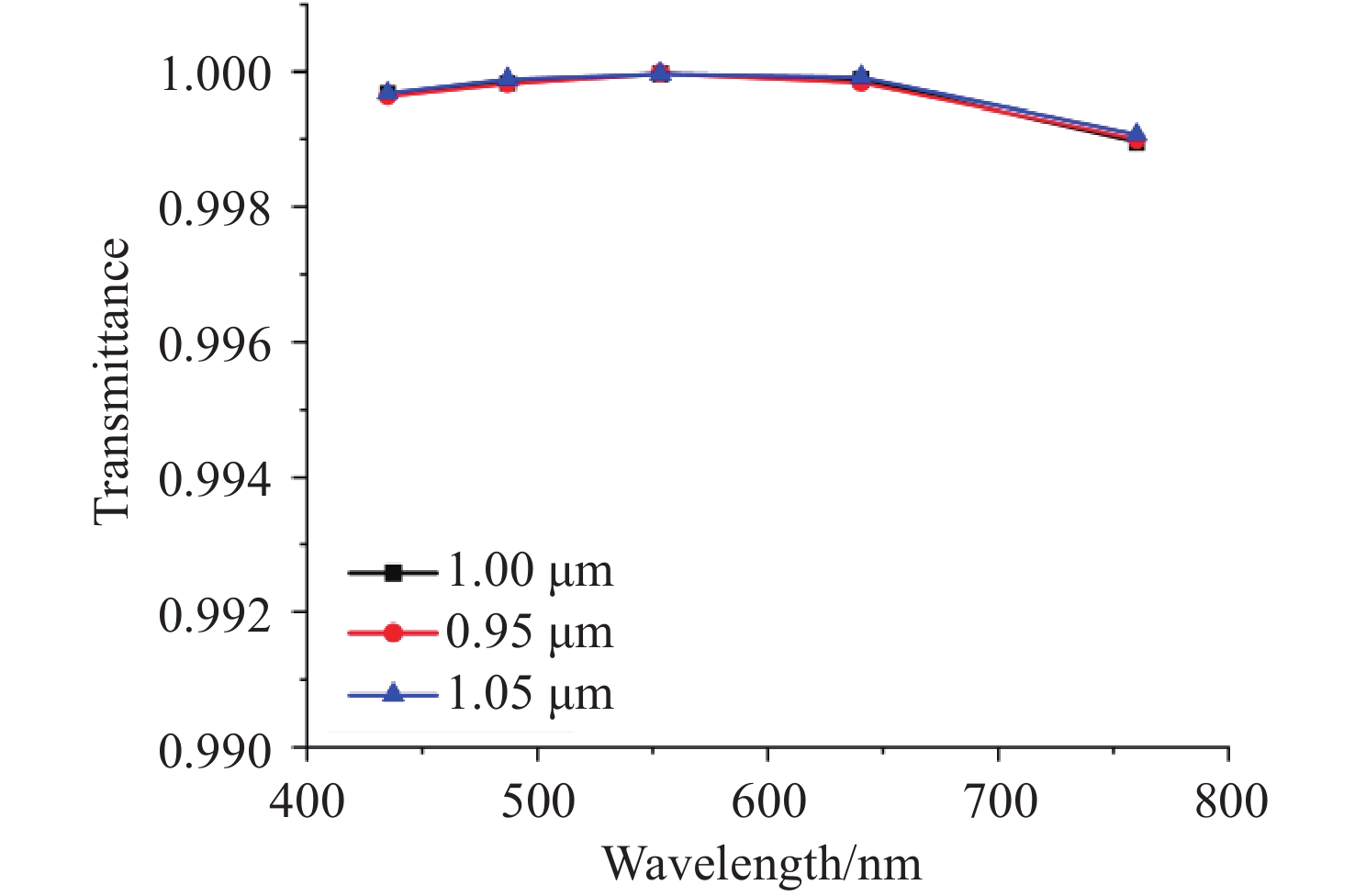
Figure 13. Variation of transmittance with (a) PML-to-edge distance and (b) PML layer count
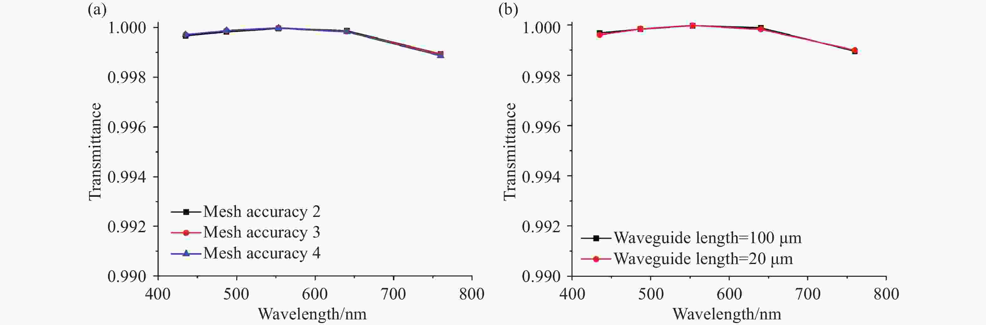
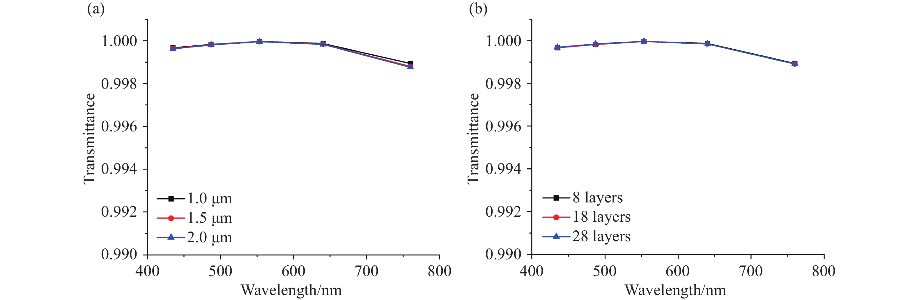
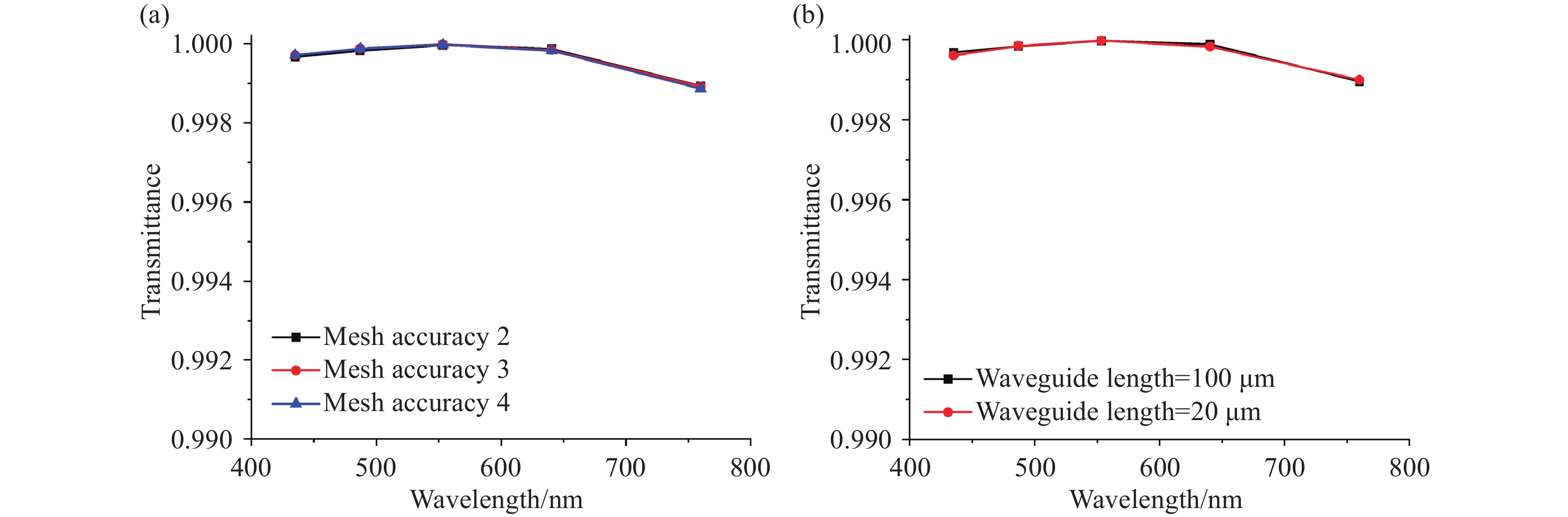
Figure 14. (a) Variation of transmittance with the mesh accuracy. (b) The transmittance for waveguide lengths of 20 µm and 100 µm
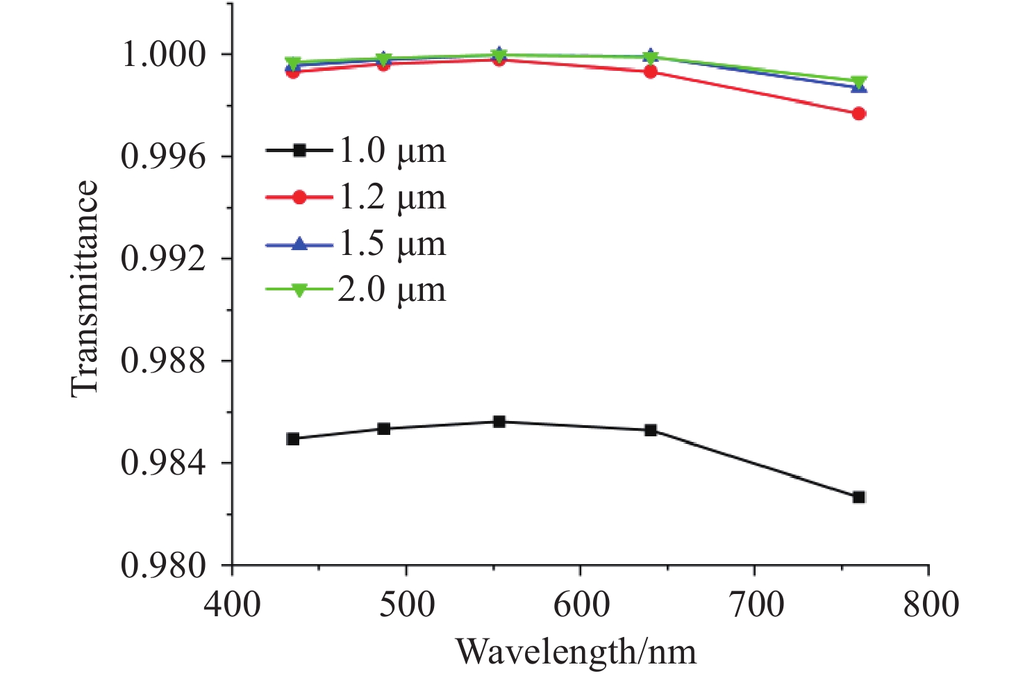
Table 1. Key parameters summary of Si3N4 full visible spectrum multimode waveguides
Slab waveguide thickness Strip waveguide width
(thickness = 1 μm)Waveguide spacing Bending radius RMS roughness
(for low-loss transmission)≥ 1 μm ≥ 2 μm ≥ 0.4 μm ≥ 10 μm ≤ 10 nm  下载: 导出CSV
-
[1] BUTT M A, IMRAN AKCA B, MATEOS X. Integrated photonic biosensors: enabling next-generation lab-on-a-chip platforms[J]. Nanomaterials, 2025, 15(10): 731. doi: 10.3390/nano15100731 [2] LIANG W Y, NAN X H, CAI W F, et al. Single-pixel infrared miniaturized spectrometer enabled by ultra-broadband reconfigurable photodetection[J]. Advanced Science, 2025, 12(25): 2500830. doi: 10.1002/advs.202500830 [3] WU N F, SUN Y X, HU J T, et al. Intelligent nanophotonics: when machine learning sheds light[J]. eLight, 2025, 5(1): 5. doi: 10.1186/s43593-025-00085-x [4] LIN Y D, YONG ZH, LUO X SH, et al. Monolithically integrated, broadband, high-efficiency silicon nitride-on-silicon waveguide photodetectors in a visible-light integrated photonics platform[J]. Nature Communications, 2022, 13(1): 6362. doi: 10.1038/s41467-022-34100-3 [5] CORATO-ZANARELLA M, JI X CH, MOHANTY A, et al. Absorption and scattering limits of silicon nitride integrated photonics in the visible spectrum[J]. Optics Express, 2024, 32(4): 5718-5728. doi: 10.1364/OE.505892 [6] CHAUHAN N, WANG J W, BOSE D, et al. Ultra-low loss visible light waveguides for integrated atomic, molecular, and quantum photonics[J]. Optics Express, 2022, 30(5): 6960-6969. doi: 10.1364/OE.448938 [7] DUAN L, STEINER T J, PINTUS P, et al. Visible-telecom entangled-photon pair generation with integrated photonics: guidelines and a materials comparison[J]. ACS Photonics, 2025, 12(1): 118-127. doi: 10.1021/acsphotonics.4c01238 [8] SIKDER P, RAHMAN M T, BAKIBILLAH A S M. Advancements and challenges of visible light communication in intelligent transportation systems: a comprehensive review[J]. Photonics, 2025, 12(3): 225. doi: 10.3390/photonics12030225 [9] HUI ZH Q, LI J Y, LI T T, et al. Study of silicon nitride waveguide-based ultra-wideband on-chip light source for OCT applications[J]. Journal of Infrared and Millimeter Waves, 2024, 43(5): 671-683. (in Chinese). doi: 10.11972/j.issn.1001-9014.2024.05.011 [10] POON J K S, GOVDELI A, SHARMA A, et al. Silicon photonics for the visible and near-infrared spectrum[J]. Advances in Optics and Photonics, 2024, 16(1): 1-59. doi: 10.1364/AOP.501846 [11] TAO Y SH, TAO Z H, LI L, et al. Silicon integrated microwave photonics[J]. Science China Information Sciences, 2025, 68(4): 140401. doi: 10.1007/s11432-025-4330-y [12] MAMMERI M, HASHEMI B, CRISCI T, et al. Single mode rib waveguide design using machine learning techniques[C]. EPJ Web of Conferences, EDP Sciences, 2024: 01010. [13] AALTO T, CHERCHI M, HARJANNE M, et al. Open-access 3-μm SOI waveguide platform for dense photonic integrated circuits[J]. IEEE Journal of Selected Topics in Quantum Electronics, 2019, 25(5): 8201109. [14] SOREF R A, SCHMIDTCHEN J, PETERMANN K. Large single-mode rib waveguides in GeSi-Si and Si-on-SiO/sub 2/[J]. IEEE Journal of Quantum Electronics, 1991, 27(8): 1971-1974. doi: 10.1109/3.83406 [15] HE J J, KOTELES E S, LAMONTAGNE B, et al. Integrated polarization compensator for WDM waveguide demultiplexers[J]. IEEE Photonics Technology Letters, 1999, 11(2): 224-226. doi: 10.1109/68.740711 [16] ZHU N. Proposal of a polarization-insensitive echelle grating demultiplexer based on a nanophotonic silicon-on-insulator platform through a dual-grating system[J]. Optics Letters, 2010, 35(10): 1599-1601. doi: 10.1364/OL.35.001599 [17] FENG D Z, QIAN W, LIANG H, et al. Fabrication insensitive echelle grating in silicon-on-insulator platform[J]. IEEE Photonics Technology Letters, 2011, 23(5): 284-286. [18] KHURANA M, DELFAN S, YI ZH H. Wafer-scale waveguide sidewall roughness scattering loss characterization by image processing[J]. Optics Express, 2025, 33(10): 20645-20655. doi: 10.1364/OE.558186 [19] LAN Y, LIU S W, CHENG CH, et al. Ultra-compact multimode waveguide bends with arbitrary bending angles[J]. Optics Express, 2025, 33(6): 13133-13144. doi: 10.1364/OE.555795 [20] YI X G, ZHANG Y B, CHEN Y, et al. On-chip silicon photonic nanohole metamaterials enabled high-density waveguide arrays[J]. Optics Express, 2024, 32(11): 19792-19800. doi: 10.1364/OE.523121 [21] CONG Q Y, LI ZH Y, ZHOU J J, et al. Process development of low-loss thick silicon nitride waveguide on 8-inch wafer[J]. Acta Photonica Sinica, 2024, 53(9): 0913002. (in Chinese). doi: 10.3788/gzxb20245309.0913002 [22] DUPONT H. Low loss silicon nitride waveguides for photonic integrated circuits[D]. Lausanne: Swiss Federal Institute of Technology, 2019: 1-52. [23] PFEIFFER M H P, KORDTS A, BRASCH V, et al. Photonic damascene process for integrated high-Q microresonator based nonlinear photonics[J]. Optica, 2016, 3(1): 20-25. doi: 10.1364/OPTICA.3.000020 [24] GRILLOT F, VIVIEN L, CASSAN E, et al. Influence of waveguide geometry on scattering loss effects in submicron strip silicon-on-insulator waveguides[J]. IET Optoelectronics, 2008, 2(1): 1-5. doi: 10.1049/iet-opt:20070001 [25] YAKUHINA A, KADOCHKIN A, SVETUKHIN V, et al. Investigation of side wall roughness effect on optical losses in a multimode Si3N4 waveguide formed on a quartz substrate[J]. Photonics, 2020, 7(4): 104. doi: 10.3390/photonics7040104 [26] LIN P T, SINGH V, LIN H Y G, et al. Low-stress silicon nitride platform for mid-infrared broadband and monolithically integrated microphotonics[J]. Advanced Optical Materials, 2013, 1(10): 732-739. doi: 10.1002/adom.201300205 -

 下载:
下载:

计量
- 文章访问数: 432
- HTML全文浏览量: 264
- PDF下载量: 33
- 被引次数: 0
