


Development of an anti-reflection coating for optical windows in multimode electro-optical detection systems
doi: 10.3724/CO.EN-2026-0012
-
摘要:
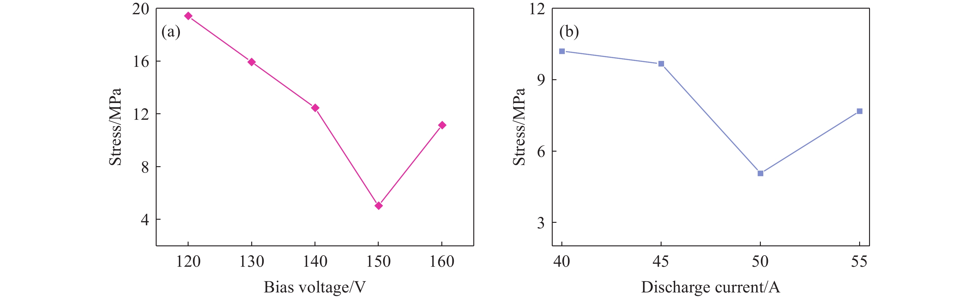
多光谱ZnS窗口作为复合光电探测系统的关键器件,可实现多波段、共光路设计。本文以多光谱ZnS为基底,设计并制备了适用于可见光、905 nm激光及长波红外多模探测应用的宽波段减反膜。系统讨论了YbF3单层膜的应力特性、制备工艺、膜系设计及误差分析,通过研究不同离子源参数对YbF3单层膜应力的影响,分析并确定了制备的最佳参数为偏压150 V,放电电流50 A。初步实验结果显示,可见光波段的平均透过率仅为73.35%,逆向分析表明,该偏差源于工具因子存在系统误差。通过修正工具因子偏差,并结合基于逆向光谱分析优化的监控方案,有效降低膜层厚度误差,实现了对高灵敏度膜层厚度的精确控制。归一化坐标分析发现,可见光与红外波段区间的光谱响应呈现显著的波长敏感度差异,本文采用针对性的单波段优化策略,并结合高灵敏度膜层的分段监控方法,以补偿多层膜沉积过程中厚度累积误差所引起的光谱偏移。测试结果表明,在0~15°入射角范围内,450~
1000 nm波段平均透过率达到93.57%,8000 ~12000 nm波段平均透过率达到92.91%,满足性能指标要求。Abstract:As a critical component of integrated optoelectronic detection systems, multispectral ZnS windows enable multiband, common-path optical configurations. In this study, a broadband anti-reflection coating was designed and fabricated on multispectral ZnS substrates for multimodal detection applications covering the visible spectrum, the 905 nm laser band, and the long-wave infrared (LWIR) region. The residual stress, deposition process, coating design, and error sources of single-layer YbF3 films were systematically investigated. By examining the effects of ion-source parameters on the stress of YbF3 films, the optimal deposition conditions were determined to be a bias voltage of 150 V and a discharge current of 50 A. Initial experiments showed that the average transmittance in the visible band was only 73.35%. Inverse analysis indicated that this deviation was mainly caused by a systematic error in the tooling factor. After correcting the tooling-factor deviation and implementing an optimized monitoring strategy based on inverse spectral analysis, the layer-thickness error was effectively reduced, enabling precise control of highly thickness-sensitive layers. Normalized-coordinate analysis further revealed pronounced wavelength-dependent differences in spectral sensitivity between the visible and infrared regions. Therefore, a targeted single-band optimization strategy, combined with segmented monitoring of highly sensitive layers, was adopted to compensate for spectral shifts induced by cumulative thickness errors during multilayer deposition. The measured results show that, within an incidence-angle range of 0-15°, the average transmittance reached 93.57% at 450-
1000 nm and 92.91% at8000 -12000 nm, satisfying the required performance specifications. -
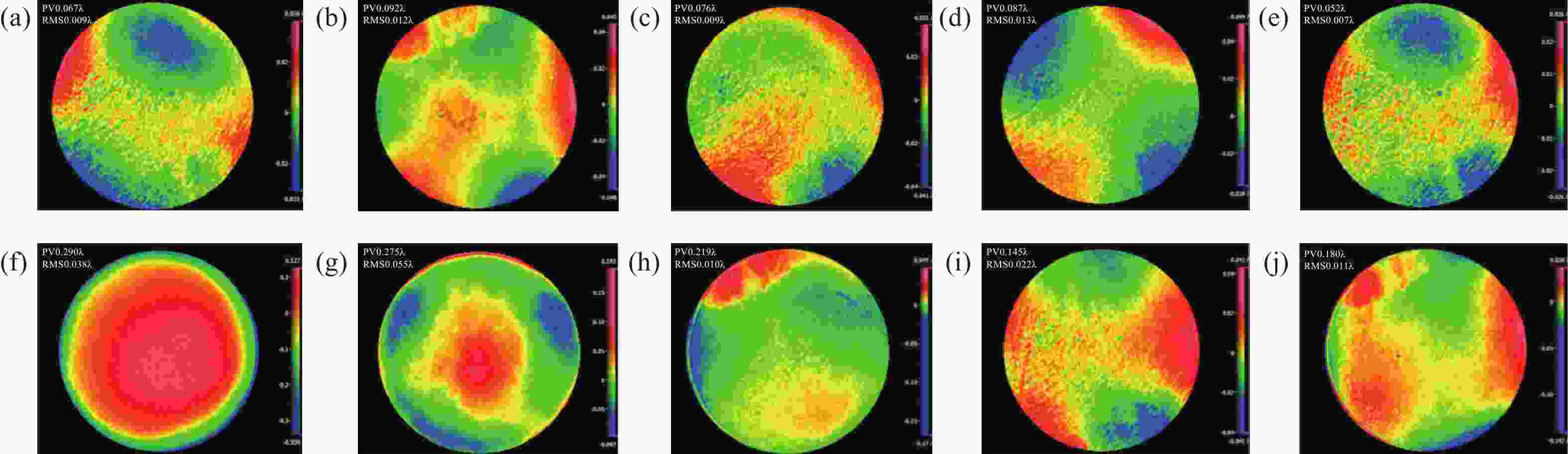
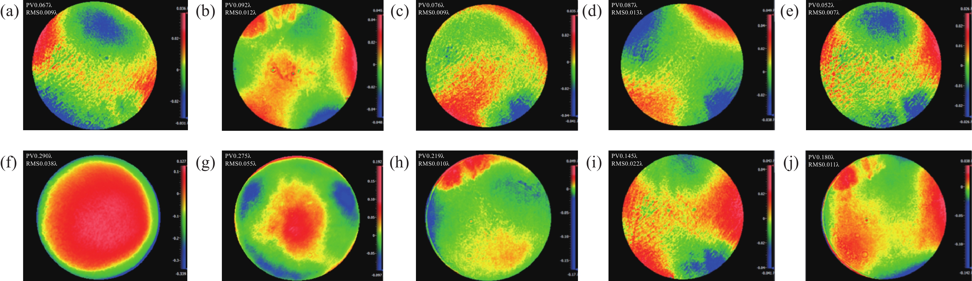
Figure 2. Surface profiles of the substrate before coating and of YbF3 films deposited under different ion-source bias voltages. (a)120 V; (b)130 V; (c)140 V; (d)150 V; (e)160 V; Surface measurement results of YbF3 films under different ion source bias voltages. (f)120 V; (g)130 V; (h)140 V; (i)150 V; (j)160 V.
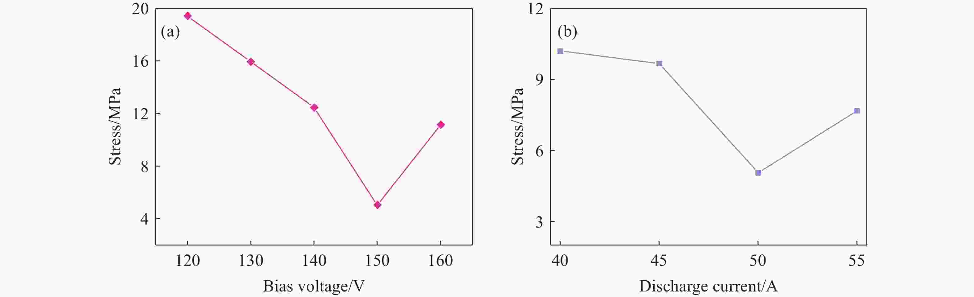
Figure 3. (a) Variation of YbF3 film stress under different ion source bias voltages; (b) Variation of YbF3 film stress under different ion source discharge currents.
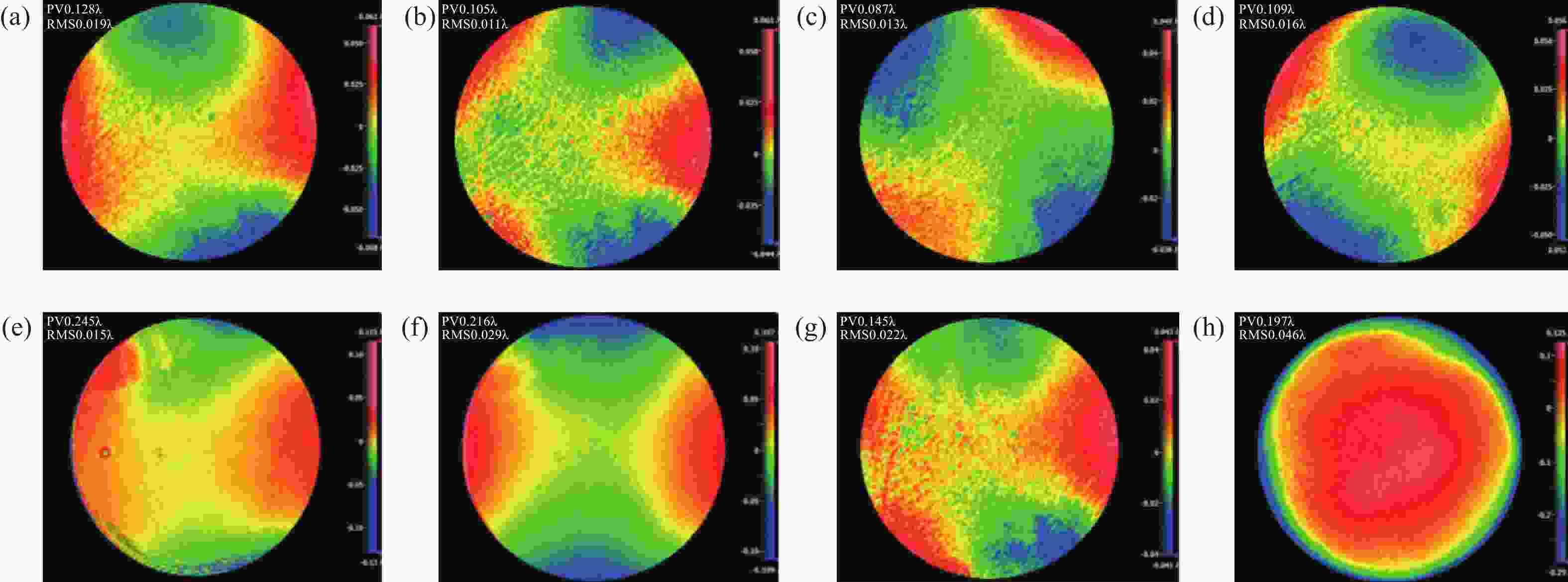
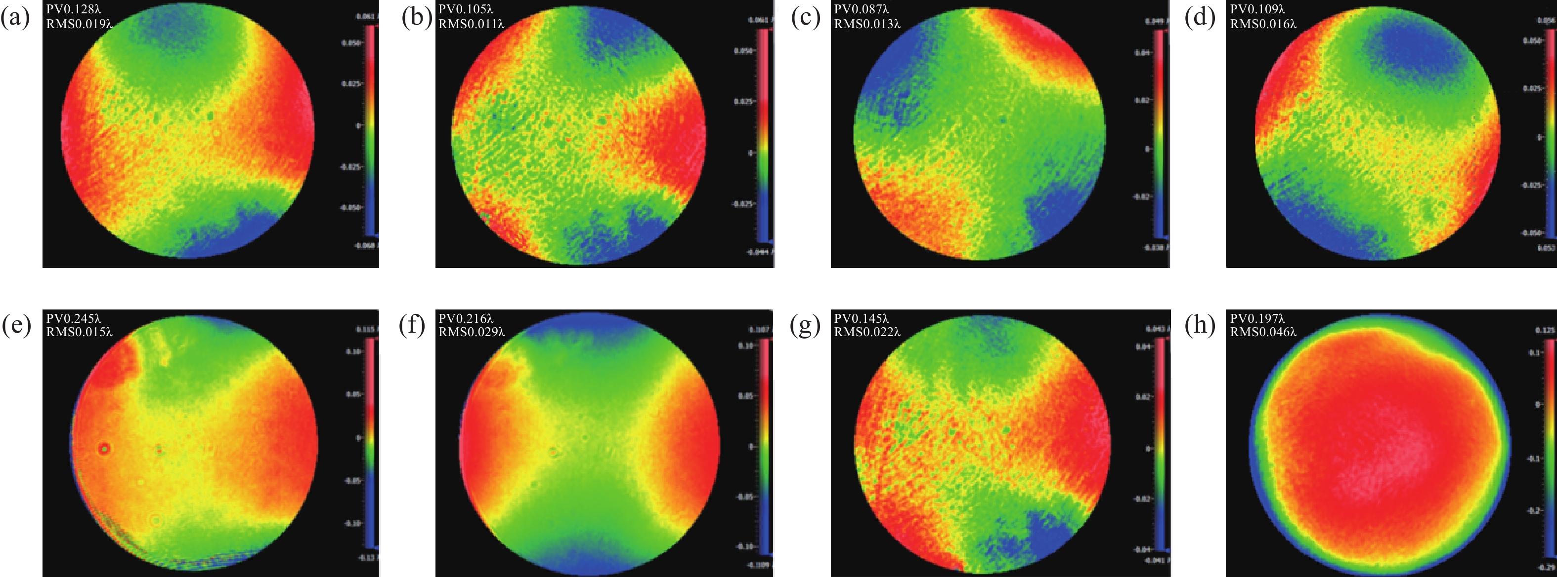
Figure 4. Surface profile of the substrate before deposition (pre-experiment). (a)40 A; (b)45 A; (c)50 A; (d)55 A. Surface measurement results of YbF3 films under different ion source discharge currents. (e)40 A; (f)45 A; (g)50 A; (h)55 A.
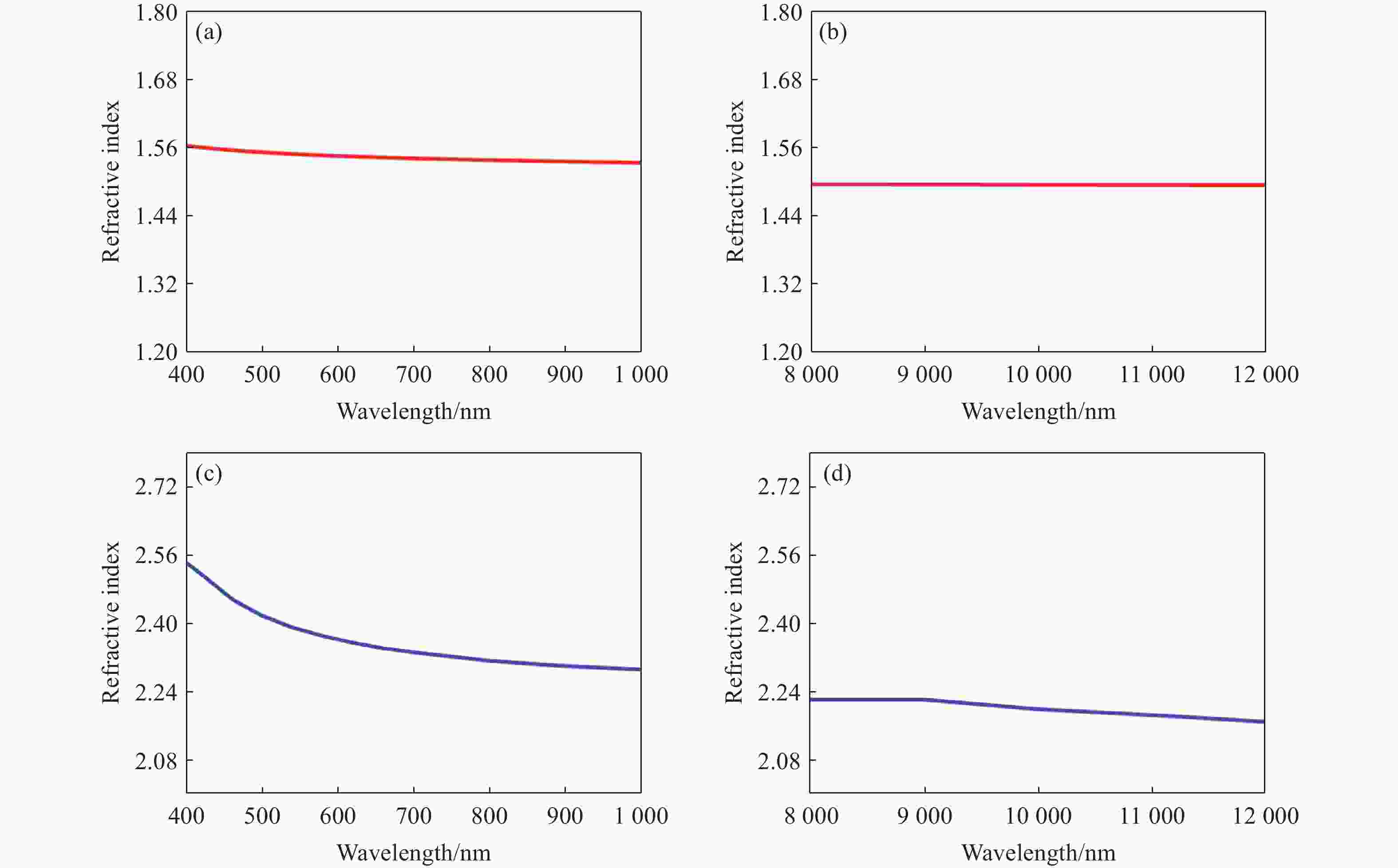
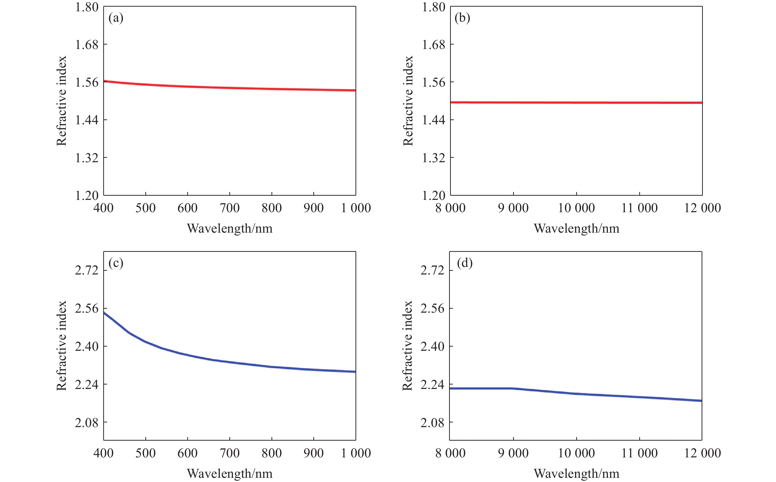
Figure 5. Refractive-index dispersion curves of YbF3 and ZnS. (a) Refractive index curve of YbF3 for 400-
1000 nm; (b) Refractive index curve of YbF3 for8000 -12000 nm; (c) Refractive index curve of ZnS for 400-1000 nm; (d) Refractive index curve of ZnS for8000 -12000 nm.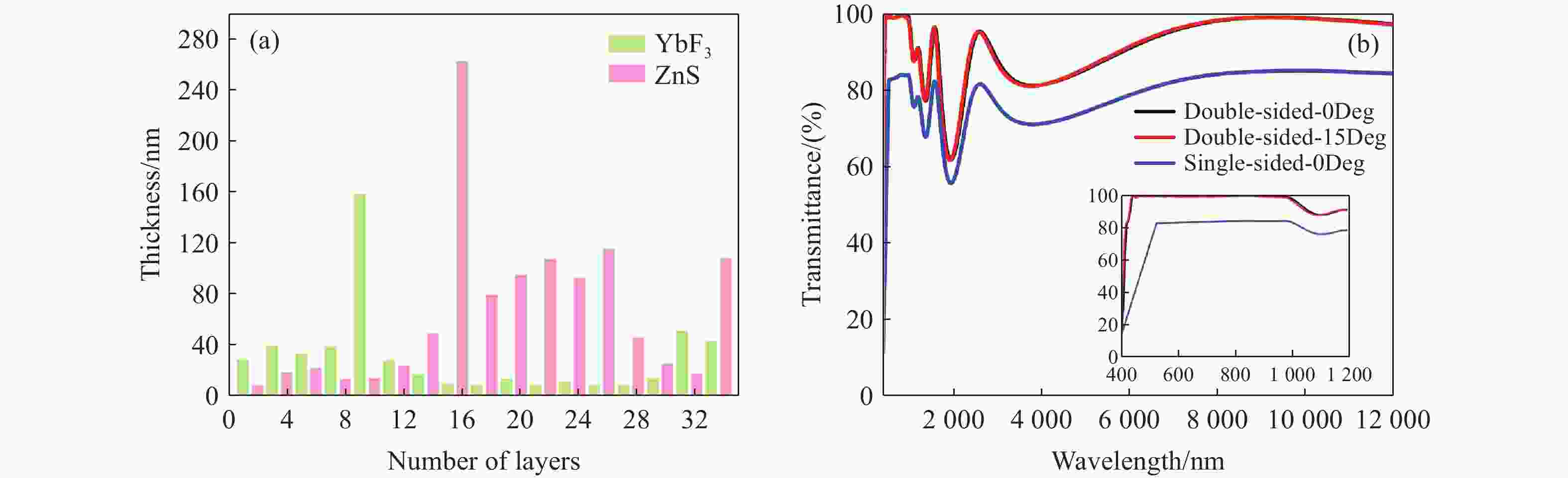
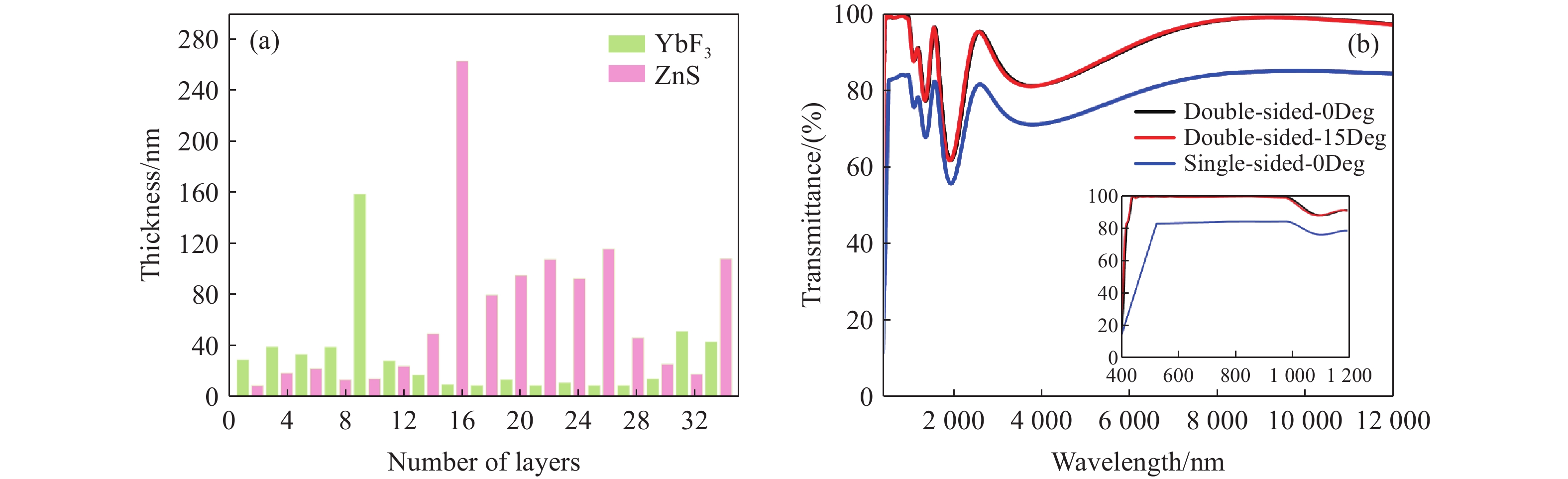
Figure 6. Layer thickness distribution of the coating stack and theoretical spectral performance of the multispectral anti-reflection coating. (a) Thickness distribution map of the multilayer coating system; (b) Theoretical spectral curve of the multispectral anti-reflection film design.
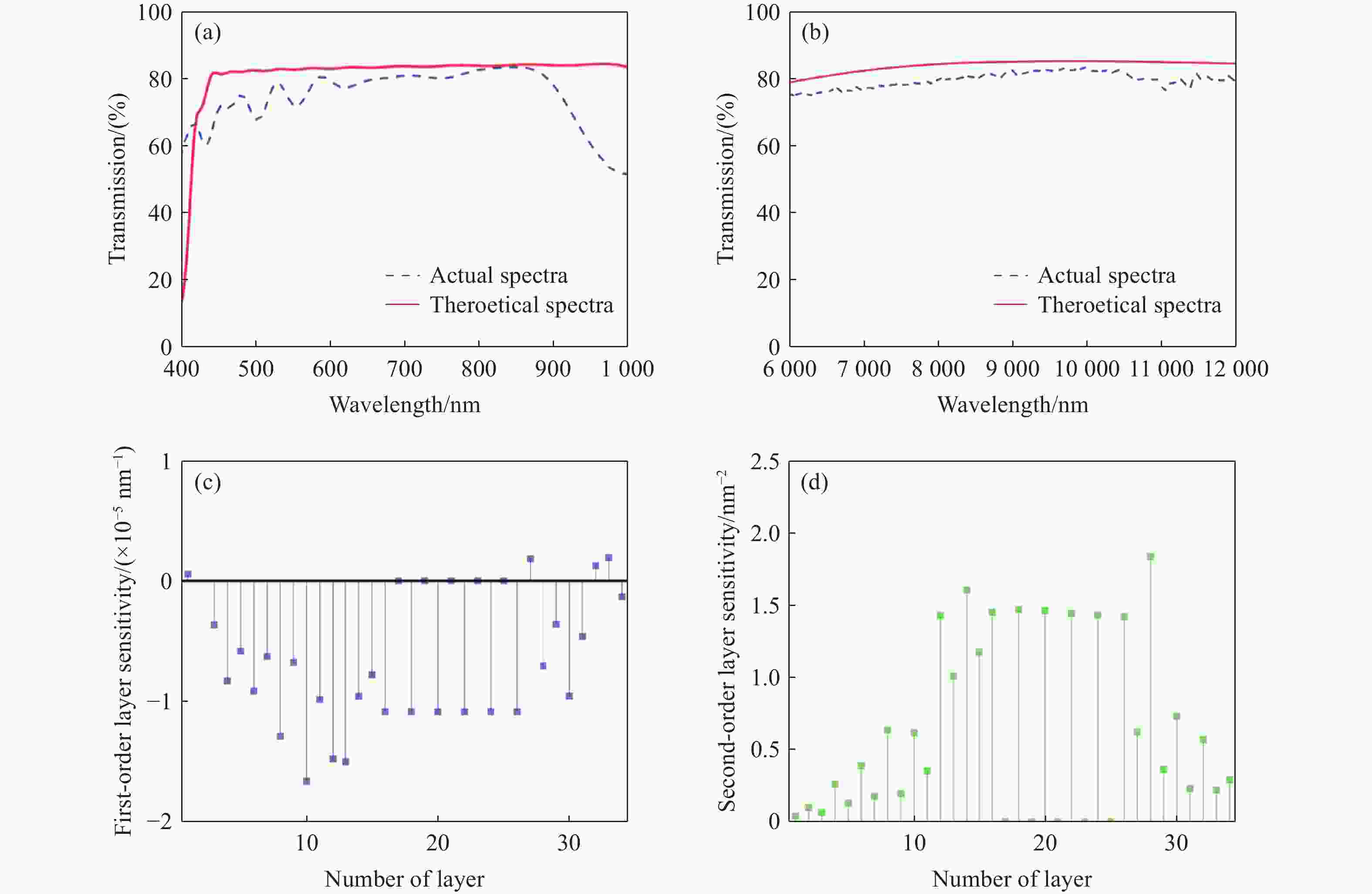
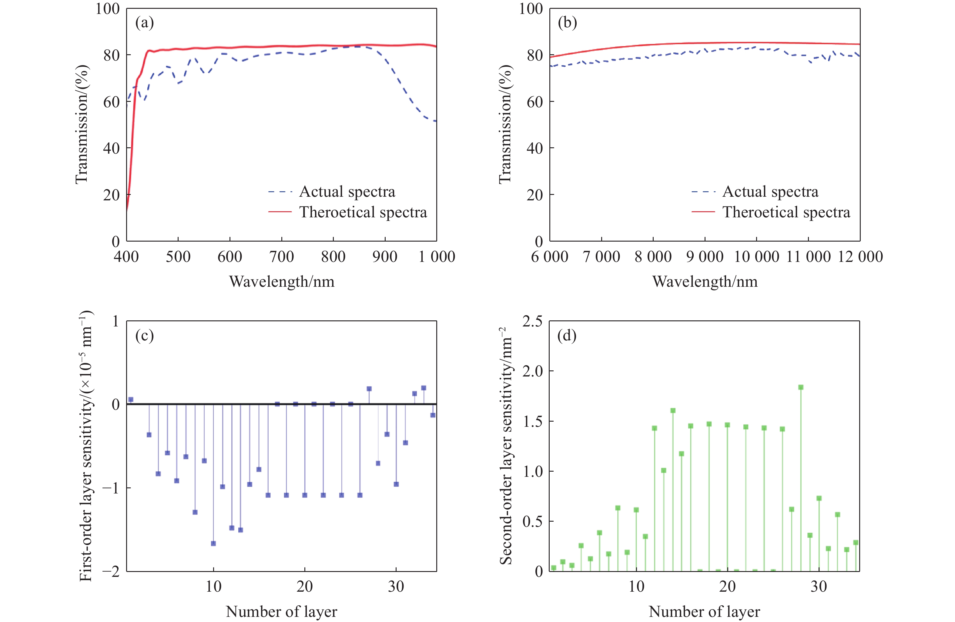
Figure 7. Measured single-sided transmittance spectra of the coating and first-order and second-order sensitivity of the coating stack. (a) Transmission test spectral curve for 400-
1000 nm; (b) Transmission test spectral curve for8000 -12000 nm; (c) First-order sensitivity; (d) Second-order sensitivity.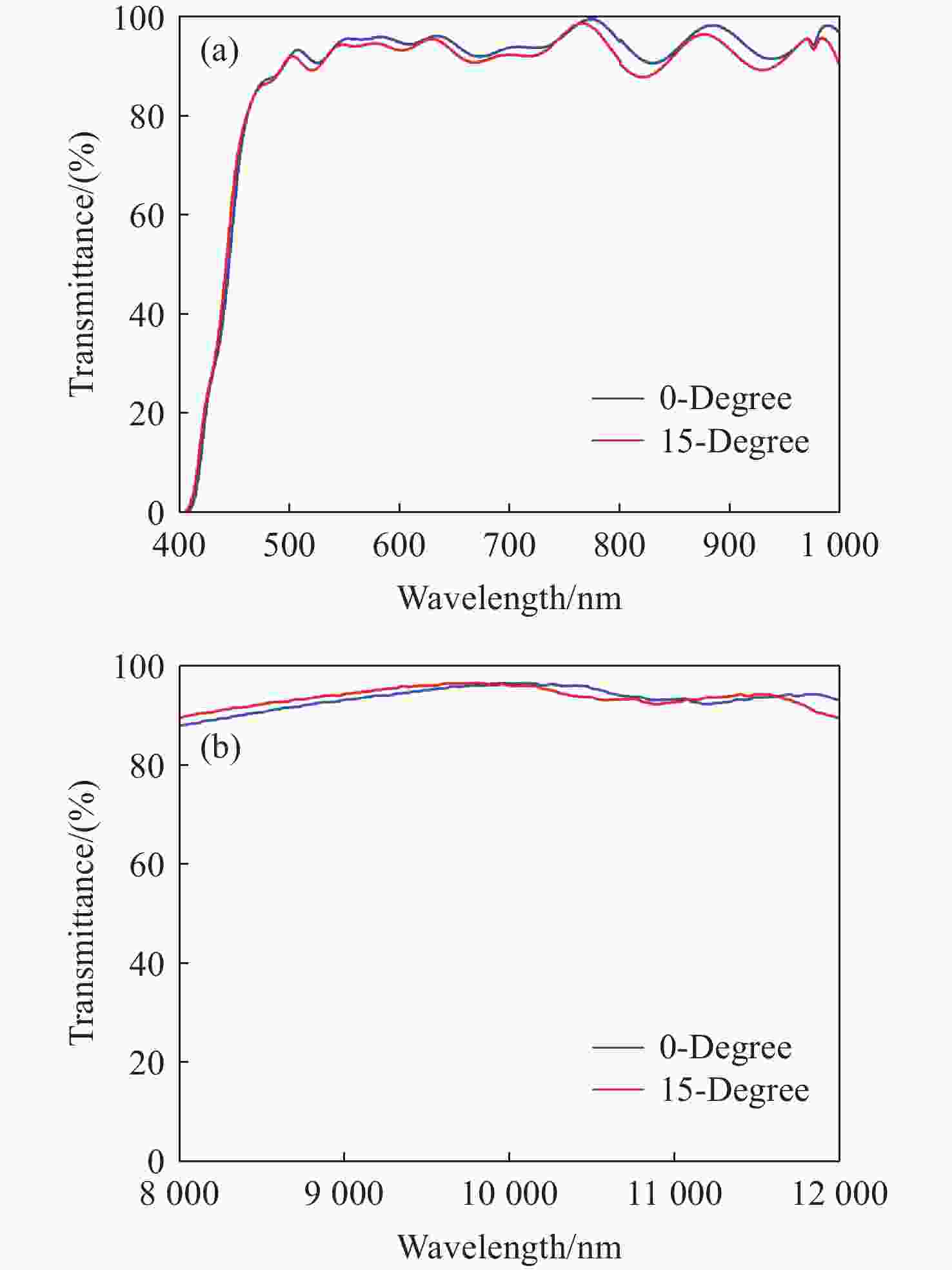
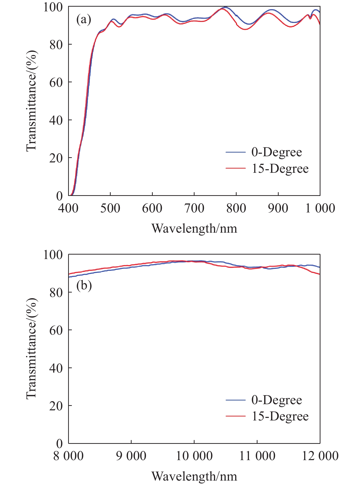
Figure 9. Measured spectral transmittance curves. (a) 0-15° transmittance spectrum over 450-
1000 nm;(b) 0-15° transmittance spectrum over8000 -12000 nm.Table 1. Deposition parameters for the control experiments.
Experiment Vacuum (mbar) Temperature
( °C)Rate (nm·s−1) APS Discharge current (A) APS Bias voltage
(V)Film thickness (nm) A 5×10⁻⁶ 120 0.5 50 120/130/
140/150/
160500 B 5×10⁻⁶ 120 0.5 40/45/
50/55150 500  下载: 导出CSV
Table 2. Deposition process parameters.
Material Deposition
temperature ( °C)Rate (nm·s−1) APS Parameters Tooling ZnS 120 0.8 - 77.5 YbF3 0.5 140 V/50 A 70.6
下载: 导出CSV
-
[1] XIN Y W, PENG Y CH, ZHANG Y X, et al. Investigation of 980/1550 nm dual-bandpass wide-cutoff filter in laser communication system[J]. Infrared Physics & Technology, 2025, 150: 105945. doi: 10.1016/j.infrared.2025.105945 [2] FU X H, JIANG H L, FU X H, et al. Study on multi-waveband infrared antireflection and protection film[J]. Acta Armamentarii, 2007, 28(10): 1183-1185. (in Chinese). doi: 10.3321/j.issn:1000-1093.2007.10.007 [3] MI G Y, ZHANG J F, HAN J, et al. Research on antireflection coating for TV, laser, mid-infrared wavebands[J]. Laser & Infrared, 2016, 46(5): 593-596. (in Chinese). doi: 10.3969/j.issn.1001-5078.2016.05.016 [4] FU X H, ZHANG G, ZHANG J, et al. Short-medium infrared detection system broadband high transmittance film[J]. Infrared and Laser Engineering, 2019, 48(10): 101700. (in Chinese). [5] WANG D SH, LI D T, FAN D, et al. Development status of space spectral imaging and integrated optical thin film technology[J]. Vacuum and Cryogenics, 2019, 25(5): 285-294. (in Chinese). doi: 10.3969/j.issn.1006-7086.2019.05.001 [6] ZHOU SH, WANG K X, LIU D Q, et al. Research on infrared dual-color filters with 3.2~3.8 μm and 4.9~5.4 μm bands[J]. Chinese Optics, 2021, 14(3): 536-543. (in Chinese). [7] LI Z Y, LIU H S, SUN P, et al. Design and preparation of laser/long-wave infrared dual-band antireflection thin film[J]. Infrared and Laser Engineering, 2022, 51(3): 202109. (in Chinese). doi: 10.3788/IRLA20210944 [8] WANG L, ZHANG SH Y, DONG J, et al. Multi-band infrared camouflage compatible with radiative cooling and visible colors via a simple multilayer film structure[J]. Optical Materials Express, 2023, 13(10): 2746-2758. doi: 10.1364/OME.497654 [9] TESLENKO A, KONSTANTINOVA T, BUSHUNOV A, et al. Antireflection microstructures on ZnSe for mid- and far-IR fabricated by femtosecond laser ablation assisted with wet chemical etching[J]. Scientific Reports, 2024, 14(1): 10743. doi: 10.1038/s41598-024-61191-3 [10] SHAVEISI M, ALIPARAST P. Design and modeling of high-performance mid-wave infrared InAsSb-based nBn photodetector using barrier band engineering approaches[J]. Frontiers of Optoelectronics, 2023, 16(1): 5. doi: 10.1007/s12200-023-00060-9 [11] MALM H, GAMFELDT A, VON WÜRTEMBERG R M, et al. High image quality type-II superlattice detector for 3.3 μm detection of volatile organic compounds[J]. Infrared Physics & Technology, 2015, 70: 34-39. doi: 10.1016/j.infrared.2014.11.013 [12] PENG Y CH, HUI B, XIN Y W, et al. Investigation into wide-angle bandpass filter for UV fluorescence imaging system[J]. Journal of Materials Science, 2025, 60(1): 339-354. doi: 10.1007/s10853-024-10546-2 [13] ZHU Y, LIU CH CH, SUN P, et al. Ultrathin, polishing-free diamond anti-reflective films for mid-wave infrared (MWIR) windows promoted by electrostatic spin-coating seeding[J]. Applied Surface Science, 2026, 722: 165554. doi: 10.1016/j.apsusc.2025.165554 [14] CIANCI E, COPPA A, FOGLIETTI V. Young's modulus and residual stress of DF PECVD silicon nitride for MEMS free-standing membranes[J]. Microelectronic Engineering, 2007, 84(5-8): 1296-1299. doi: 10.1016/j.mee.2007.01.056 [15] ZHANG Q Y, LI X L, SHEN J, et al. ZrO2 thin films and ZrO2/SiO2 optical reflection filters deposited by sol-gel method[J]. Materials Letters, 2000, 45(6): 311-314. doi: 10.1016/S0167-577X(00)00124-5 [16] JENSEN T R, WARREN J, JOHNSON R L. Ion-assisted deposition of moisture-stable hafnium oxide films for ultraviolet applications[J]. Applied Optics, 2002, 41(16): 3205-3210. doi: 10.1364/AO.41.003205 [17] SAFIN R G, GAĬNUTDINOV I S, SABIROV R S, et al. Solar-blind filter for the ultraviolet region[J]. Journal of Optical Technology, 2007, 74(3): 208-210. doi: 10.1364/jot.74.000208 [18] HITOSHI U. On-beam-assisted deposition of hard cBN films and internal stress relaxation by laminated layer[J]. Kaken, 2018, 1800123. (查阅网上资料, 未能确认文献类型, 请确认文献类型及格式是否正确). [19] MUKAI K, HUJITA S, TAKAYAMA S. Change of an internal stress exerted on each layer in AZO/Cu/Mo multilayered films on annealing[J]. Journal of the Electrochemical Society, 2022, 169(12): 122502. doi: 10.1149/1945-7111/aca6aa [20] ZHANG SH, LIU B, ZHANG X, et al. Reduction of internal stress in InGaZnO (IGZO) thin film transistors by ultra-thin metal oxide layer[J]. Materials Science in Semiconductor Processing, 2024, 173: 108093. doi: 10.1016/j.mssp.2023.108093 [21] ZHU H, JIANG H Y, GUO K, et al. Development of wide-angle depolarizing reflector at 1064 nm[J]. Materials, 2023, 16(12): 4258. doi: 10.3390/ma16124258 [22] HONG I S, HWANG Y S, LEE G H, et al. Ion-beam characteristics of novel helicon ion sources for different plasma parameters[J]. Review of Scientific Instruments, 2000, 71(3): 1385-1388. doi: 10.1063/1.1150467 [23] KLIMOV A, BAKEEV I, OKS E, et al. Forevacuum plasma source of continuous electron beam[J]. Laser and Particle Beams, 2019, 37(2): 203-208. doi: 10.1017/S0263034619000375 [24] ÖZHAN A E S, HACALOĞLU T, KAFTANOĞLU B. Development of hard, anti-reflective coating for mid wave infrared region[J]. Infrared Physics & Technology, 2021, 119: 103910. doi: 10.1016/j.infrared.2021.103910 [25] SAID S A M, AL-AQEELI N, WALWIL H M. The potential of using textured and anti-reflective coated glasses in minimizing dust fouling[J]. Solar Energy, 2015, 113: 295-302. doi: 10.1016/j.solener.2015.01.007 [26] FU X H, ZHANG Y SH, KOU Y, et al. Study and fabrication of multi-channel filter film in free-space laser communication system[J]. Chinese Journal of Lasers, 2015, 42(4): 0407001. (in Chinese). doi: 10.3788/CJL201542.0407001 [27] XIONG SH F, FU X H, LIU D M, et al. Narrow-band filter based on infrared absorption characteristics of methane gas[J]. Acta Photonica Sinica, 2017, 46(10): 1023003. (in Chinese). doi: 10.3788/gzxb20174610.1023003 [28] CAO X Y, ZHANG Y X, WANG B, et al. Integrated symmetric equivalent layer design and stress compensation for high-performance infrared dual-band depolarizing beam splitters[J]. Infrared Physics & Technology, 2026, 155: 106460. doi: 10.1016/j.infrared.2026.106460 -

 下载:
下载:

计量
- 文章访问数: 81
- HTML全文浏览量: 55
- PDF下载量: 7
- 被引次数: 0
