| Citation: | CHENG Yan-ling, DU Ling-yan, YIN Jie, CHEN Fu-song, XU Shun-yang. Effect of picosecond laser energy density on the photoelectric properties of se-doped silicon[J]. Chinese Optics. doi: 10.37188/CO.2026-0103

|
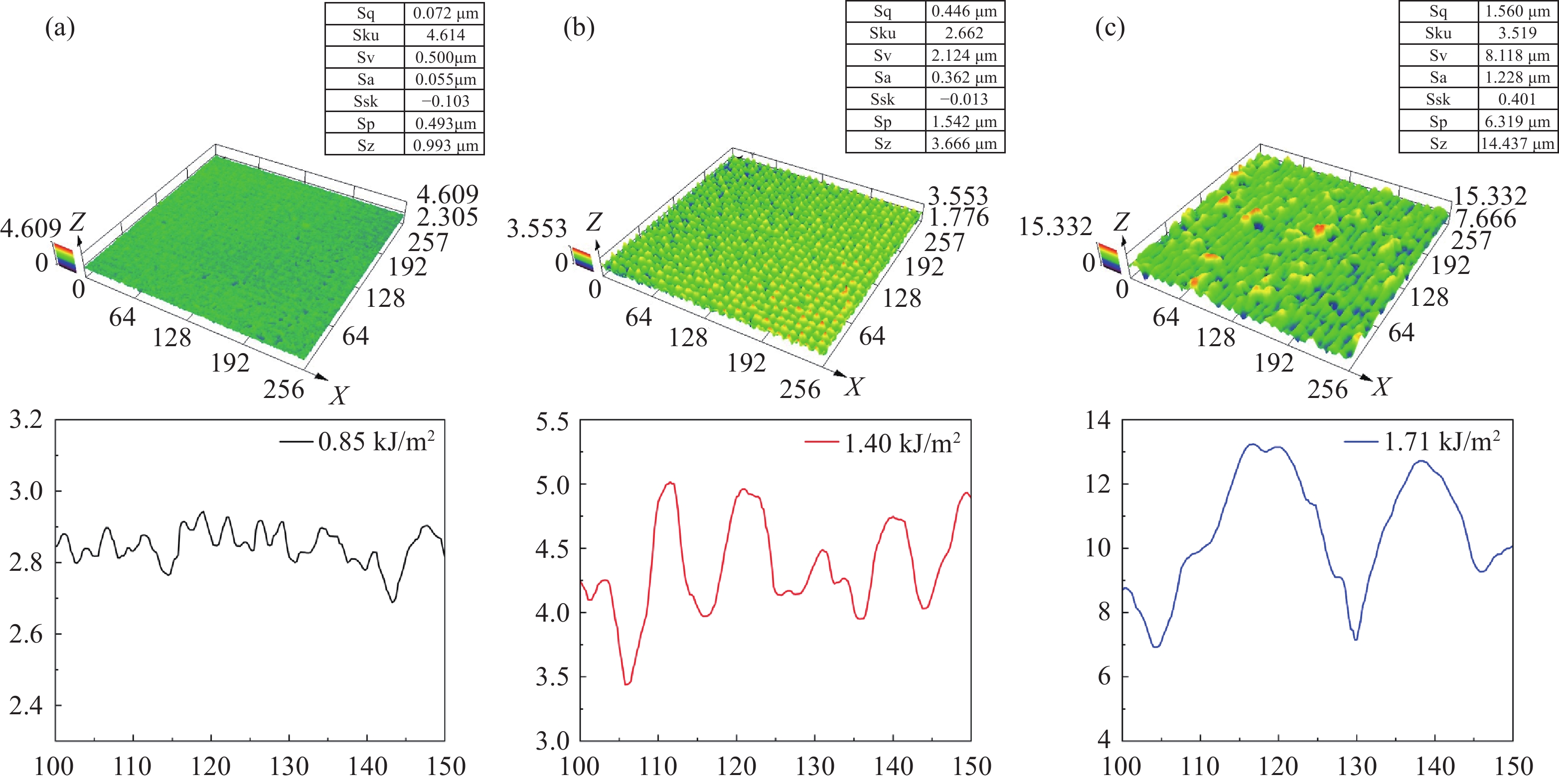
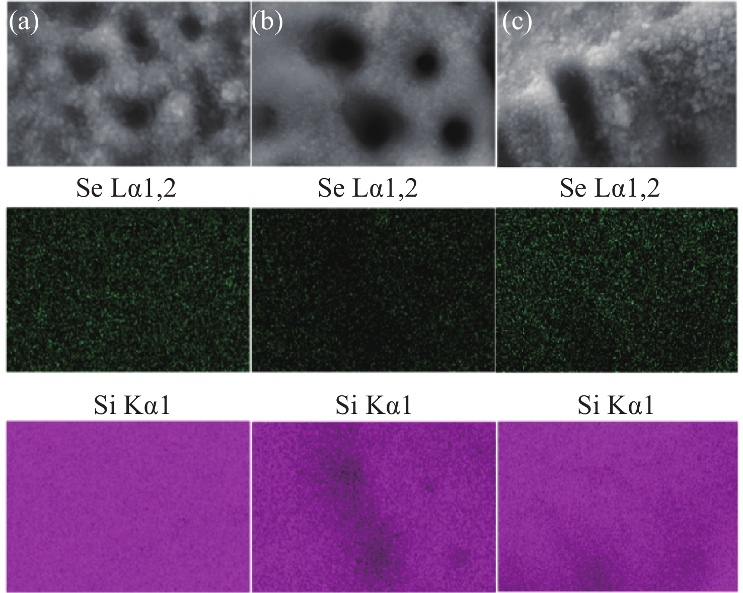
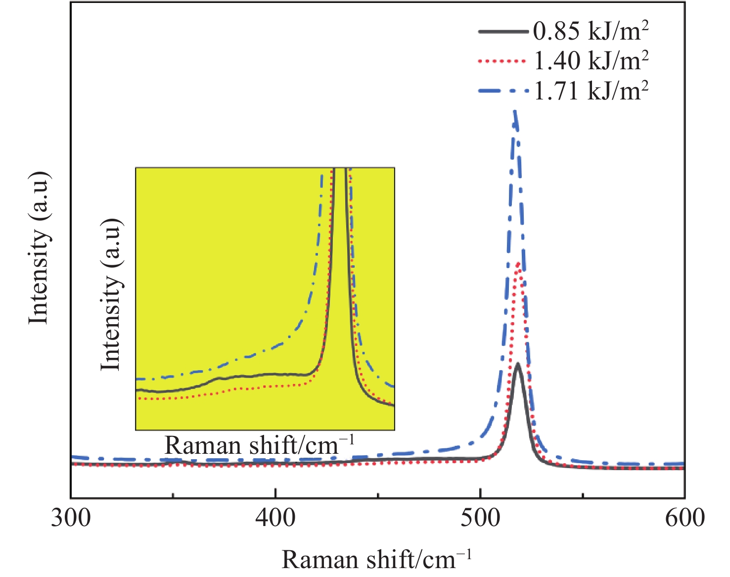
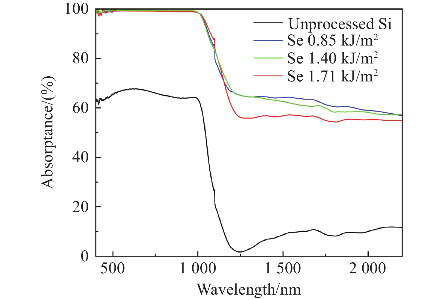
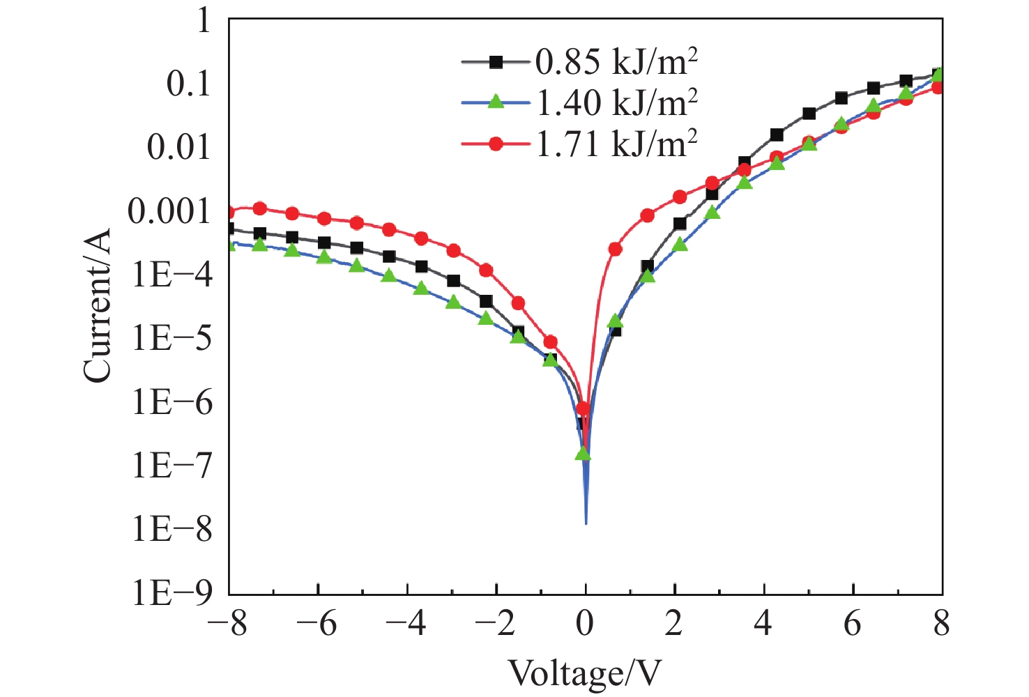
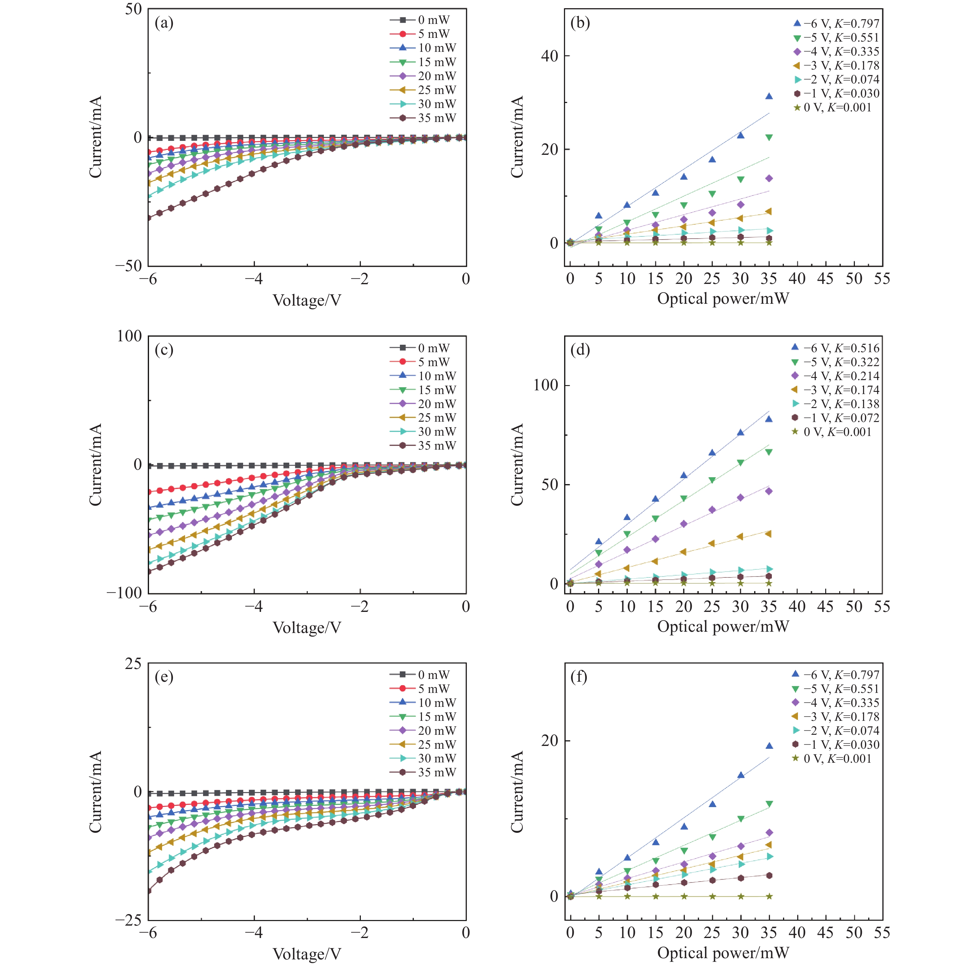
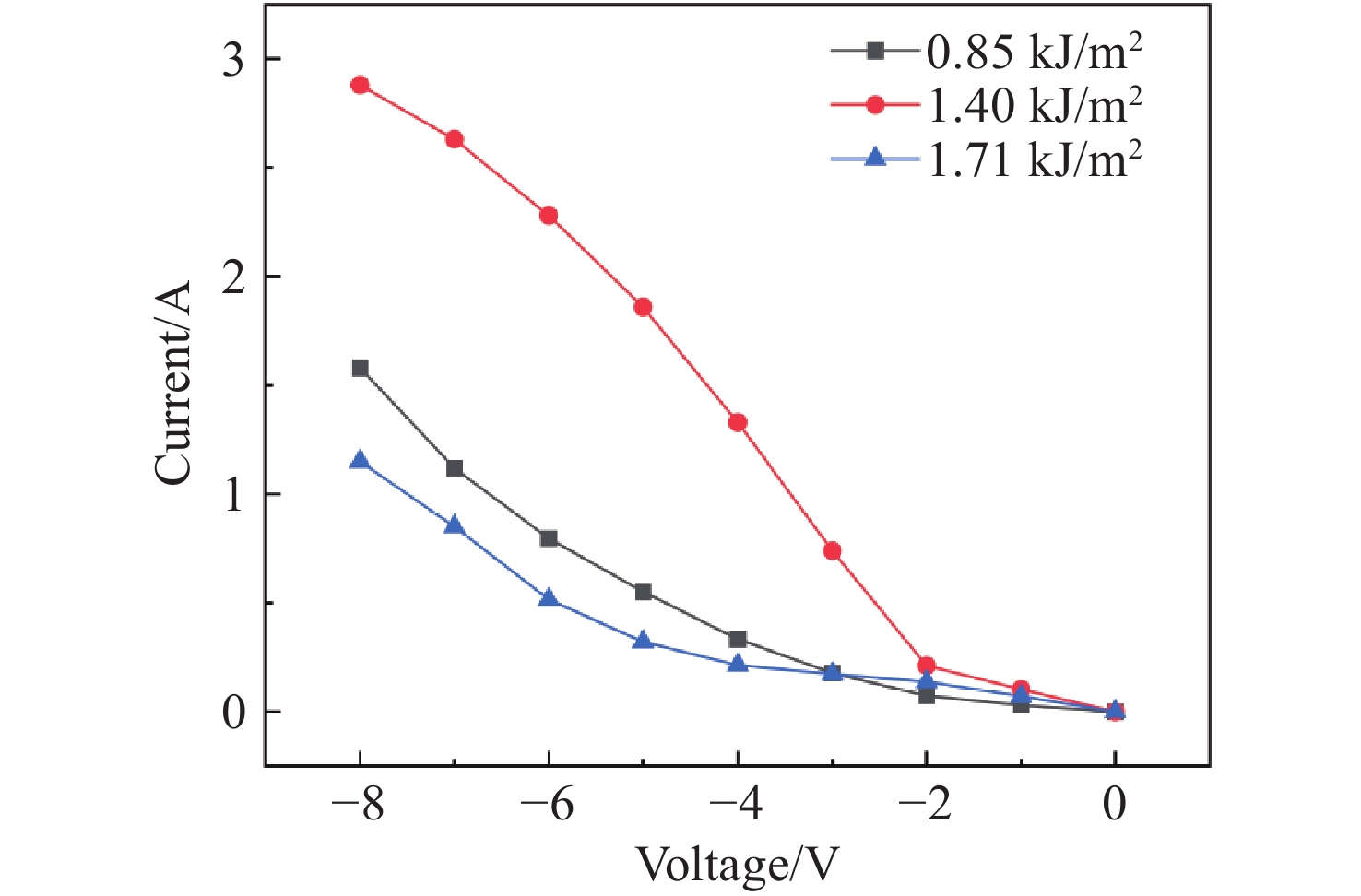
The near-infrared optical absorption and photoresponse of silicon-based optoelectronic devices are intrinsically limited by the bandgap of silicon. Picosecond laser-induced Se doping combined with surface micro/nanostructuring provides an effective approach to enhancing the near-infrared performance of silicon. Among the relevant processing parameters, laser energy density plays a critical role in governing microstructure evolution and dopant redistribution, thereby strongly influencing device performance. In this study, single-crystal silicon substrates coated with a Se film were irradiated using a picosecond laser at energy densities of 0.85, 1.40, and 1.71 kJ/m2. Se-doped N+−N silicon photodiodes were subsequently fabricated to systematically investigate the effects of laser energy density on surface micro/nanostructure, optical absorptance, and photoelectric performance. The results show that the overall crystalline structure of the samples remains well preserved under all processing conditions, whereas their surface microstructures differ markedly. These structural variations further affect the optical absorption and device photoresponse. At an energy density of 1.40 kJ/m2, the sample exhibits the most uniform surface micro/nanostructure. Optical and electrical measurements show that its near-infrared absorptance exceeds 60%, while the corresponding photodiode achieves a responsivity of 2.28 A/W at a reverse bias of −6 V under

| [1] |
LV J, ZHANG T, ZHANG P, et al. Review application of nanostructured black silicon[J]. Nanoscale Research Letters, 2018, 13(1): 110. doi: 10.1186/s11671-018-2523-4
|
| [2] |
TONG ZH Y, BU M X, ZHANG Y Q, et al. Hyperdoped silicon: processing, properties, and devices[J]. Journal of Semiconductors, 2022, 43(9): 093101. doi: 10.1088/1674-4926/43/9/093101
|
| [3] |
LI D D, KONG L H, FENG L P, et al. Large-area, high-resolution, flexible x-ray scintillator film based on a novel 0d hybrid cuprous halide[J]. Light: Advanced Manufacturing, 2025, 6(4): 44. doi: 10.37188/lam.2025.044
|
| [4] |
GAO D, CHEN B J, SHA X ZH, et al. Near infrared emissions from both high efficient quantum cutting (173%) and nearly-pure-color upconversion in NaY(WO4)2: Er3+/Yb3+ with thermal management capability for silicon-based solar cells[J]. Light: Science & Applications, 2024, 13(1): 17.
|
| [5] |
LONG J B, WANG ZH K, PENG H F, et al. A chip-based optoelectronic-oscillator frequency comb[J]. eLight, 2025, 5(1): 14. doi: 10.1186/s43593-025-00094-w
|
| [6] |
WANG H, CHEN L, WU Y, et al. Advancing inorganic electro-optical materials for 5 G communications: from fundamental mechanisms to future perspectives[J]. Light: Science & Applications, 2025, 14(1): 190.
|
| [7] |
GREEN M A. Silicon Solar Cells: Advanced Principles & Practice[M]. Kensington: Centre for Photovoltaic Devices and Systems, University of New South Wales, 1995.
|
| [8] |
SZE S M, LI Y M, NG K K. Physics of Semiconductor Devices[M]. 4th ed. Hoboken: John Wiley & Sons, 2021.
|
| [9] |
LIU X G, COXON P R, PETERS M, et al. Black silicon: fabrication methods, properties and solar energy applications[J]. Energy & Environmental Science, 2014, 7(10): 3223-3263. doi: 10.1039/C4EE01152J
|
| [10] |
FAN ZH, CUI D F, ZHANG Z X, et al. Recent progress of black silicon: from fabrications to applications[J]. Nanomaterials, 2021, 11(1): 41. doi: 10.3390/nano11010041
|
| [11] |
SUGIOKA K, CHENG Y. Ultrafast lasers-reliable tools for advanced materials processing[J]. Light: Science & Applications, 2014, 3(4): e149.
|
| [12] |
PHILLIPS K C, GANDHI H H, MAZUR E, et al. Ultrafast laser processing of materials: a review[J]. Advances in Optics and Photonics, 2015, 7(4): 684-712. doi: 10.1364/AOP.7.000684
|
| [13] |
ZHAO ZH CH, KRAVTSOV V, WANG Z R, et al. Applications of ultrafast nano-spectroscopy and nano-imaging with tip-based microscopy[J]. eLight, 2025, 5(1): 1. doi: 10.1186/s43593-024-00079-1
|
| [14] |
ZHAO J H, LI X B, CHEN Q D, et al. Ultrafast laser-induced black silicon, from micro-nanostructuring, infrared absorption mechanism, to high performance detecting devices[J]. Materials Today Nano, 2020, 11: 100078. doi: 10.1016/j.mtnano.2020.100078
|
| [15] |
LI CH, ZHAO J H, CHEN ZH G. Infrared absorption and sub-bandgap photo-response of hyperdoped silicon by ion implantation and ultrafast laser melting[J]. Journal of Alloys and Compounds, 2021, 883: 160765. doi: 10.1016/j.jallcom.2021.160765
|
| [16] |
FU J W, YANG D R, YU X G. Hyperdoped crystalline silicon for infrared photodetectors by pulsed laser melting: a review[J]. Physica Status Solidi (a), 2022, 219(14): 2100772. doi: 10.1002/pssa.202100772
|
| [17] |
HUANG S, JIN X R, WU Q, et al. Ultrafast laser hyperdoped black silicon and its application in photodetectors: a review[J]. Physica Status Solidi (a), 2024, 221(24): 2400127. doi: 10.1002/pssa.202400127
|
| [18] |
UMEZU I, WARRENDER J M, CHARNVANICHBORIKARN S, et al. Emergence of very broad infrared absorption band by hyperdoping of silicon with chalcogens[J]. Journal of Applied Physics, 2013, 113(21): 213501. doi: 10.1063/1.4804935
|
| [19] |
HER T H, FINLAY R J, WU C, et al. Microstructuring of silicon with femtosecond laser pulses[J]. Applied Physics Letters, 1998, 73(12): 1673-1675. doi: 10.1063/1.122241
|
| [20] |
SHEEHY M A, TULL B R, FRIEND C M, et al. Chalcogen doping of silicon via intense femtosecond-laser irradiation[J]. Materials Science and Engineering: B, 2007, 137(1-3): 289-294. doi: 10.1016/j.mseb.2006.10.002
|
| [21] |
HU SH X, HAN P D, WANG SH, et al. Improved photoresponse characteristics in Se-doped Si photodiodes fabricated using picosecond pulsed laser mixing[J]. Semiconductor Science and Technology, 2012, 27(10): 102002. doi: 10.1088/0268-1242/27/10/102002
|
| [22] |
DU L Y, YIN J, ZENG W, et al. Fabrication of micro-nano structure Se-doped silicon via picosecond laser irradiation assisted by dopant film[J]. Materials Letters, 2023, 331: 133463. doi: 10.1016/j.matlet.2022.133463
|
| [23] |
GUO H, XIE J W, HE G ZH, et al. A review of ultrafast laser micro/nano fabrication: material processing, surface/interface controlling, and devices fabrication[J]. Nano Research, 2024, 17(7): 6212-6230. doi: 10.1007/s12274-024-6644-z
|
| [24] |
GROSS J M, SHAVANDI S R, ZAGORAC T, et al. Picosecond versus femtosecond-laser ablation of silicon in atmosphere[J]. Journal of Laser Applications, 2023, 35(4): 042053. doi: 10.2351/7.0001206
|
| [25] |
HAMAD A H. Effects of different laser pulse regimes (nanosecond, picosecond and femtosecond) on the ablation of materials for production of nanoparticles in liquid solution[M]//VISKUP R. High Energy and Short Pulse Lasers. Rijeka: InTech, 2016.
|
| [26] |
ZHOU SH Q, LIU F, PRUCNAL S, et al. Hyperdoping silicon with selenium: solid vs. liquid phase epitaxy[J]. Scientific Reports, 2015, 5(1): 8329. doi: 10.1038/srep08329
|
| [27] |
WANG M, DEBERNARDI A, ZHANG W X, et al. Critical behavior of the insulator-to-metal transition in Te-hyperdoped Si[J]. Physical Review B, 2020, 102(8): 085204. doi: 10.1103/PhysRevB.102.085204
|
| [28] |
DU L Y, LIU SH P, CHEN F S, et al. Effects of dopant film thickness on near-infrared photodiode response based on Se-doped silicon fabricated by picosecond laser[J]. Infrared Physics & Technology, 2025, 150: 105933. doi: 10.1016/j.infrared.2025.105933
|
| [29] |
ATTEIA F, LE ROUZO J, DENAIX L, et al. Morphologies and optical properties of black silicon by room temperature reactive ion etching[J]. Materials Research Bulletin, 2020, 131: 110973. doi: 10.1016/j.materresbull.2020.110973
|
| [30] |
ZHANG X M, LI W N, JIN CH, et al. Effects of black silicon surface morphology induced by a femtosecond laser on absorptance and photoelectric response efficiency[J]. Photonics, 2024, 11(10): 947. doi: 10.3390/photonics11100947
|
| [31] |
KOMAROV F, PARKHOMENKO I, ALZHANOVA A, et al. Broad infrared absorption band through ion beam hyperdoping of silicon with selenium[J]. Applied Surface Science, 2023, 639: 158168. doi: 10.1016/j.apsusc.2023.158168
|
| [32] |
LEDINSKÝ M, FEKETE L, STUCHLÍK J, et al. Characterization of mixed phase silicon by Raman spectroscopy[J]. Journal of Non-Crystalline Solids, 2006, 352(9-20): 1209-1212. doi: 10.1016/j.jnoncrysol.2005.10.072
|
| [33] |
FANG Y J, ARMIN A, MEREDITH P, et al. Accurate characterization of next-generation thin-film photodetectors[J]. Nature Photonics, 2019, 13(1): 1-4. doi: 10.1038/s41566-018-0288-z
|

Figures(8)




 DownLoad: