| Citation: | ZOU Jing-chen, LUO Peng, MA Xu, ZHAO Yi-hui. Low-loss waveguide design for full visible spectrum on-chip photonic devices[J]. Chinese Optics, 2026, 19(3): 715-729. doi: 10.37188/CO.EN-2025-0036

|
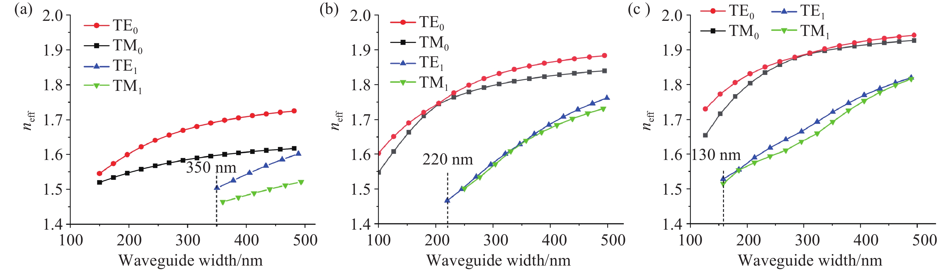
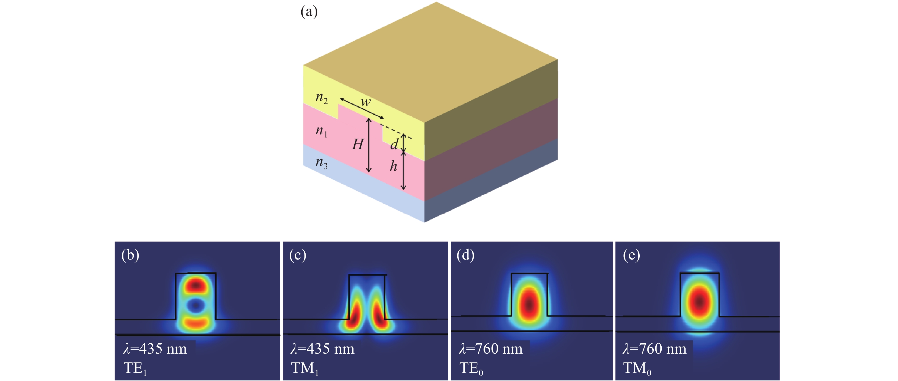
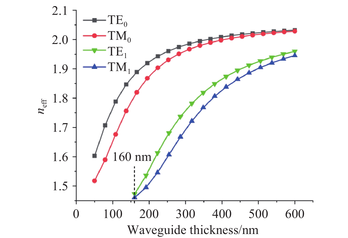
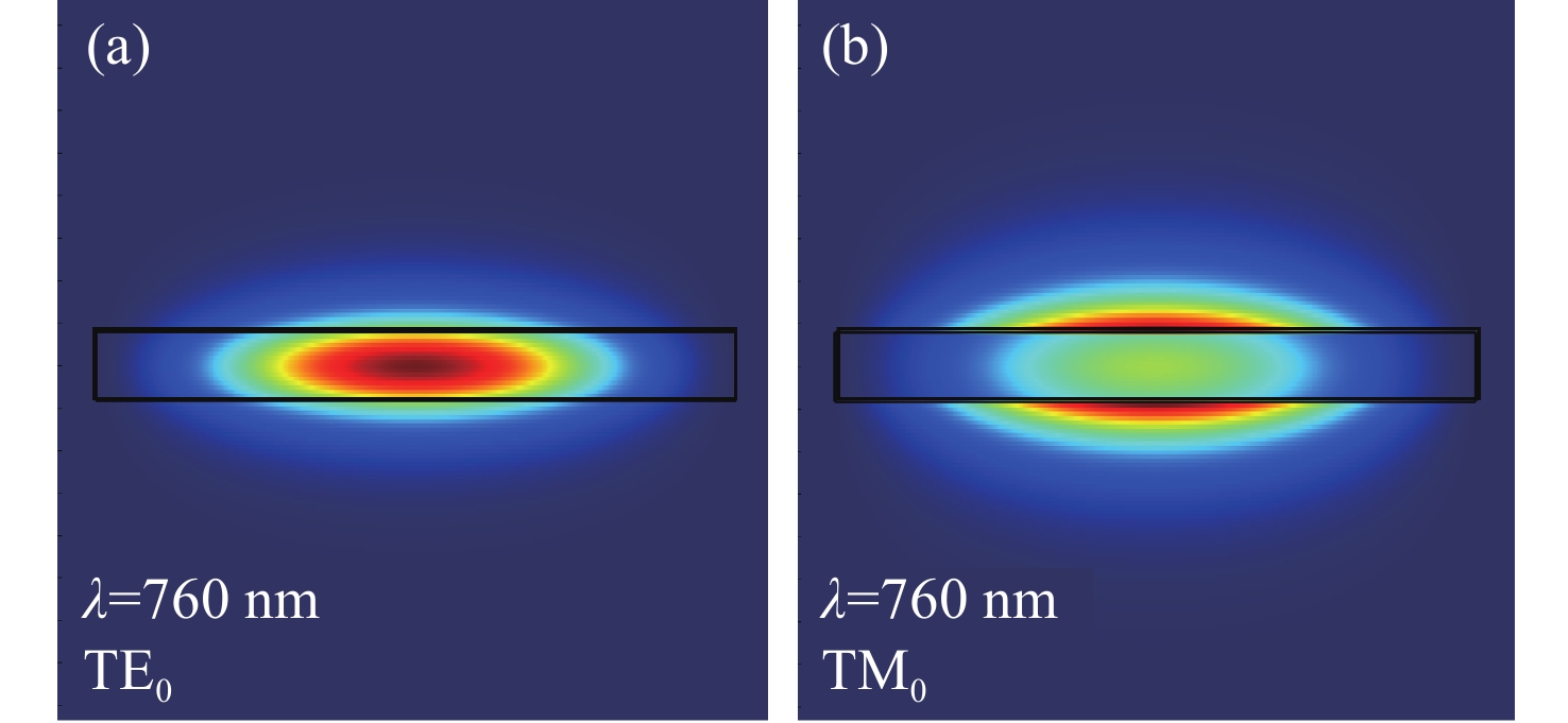
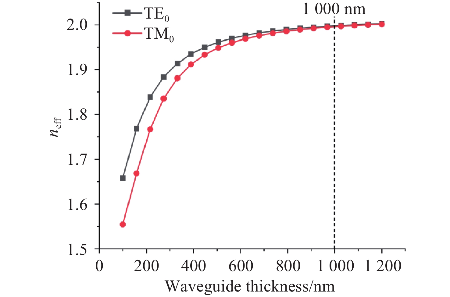
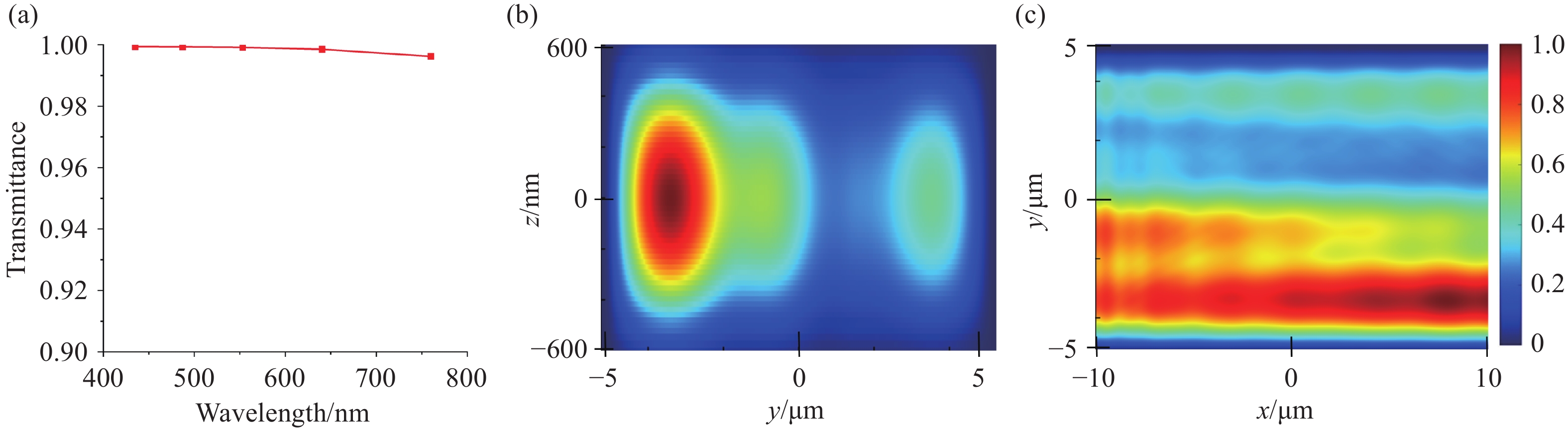
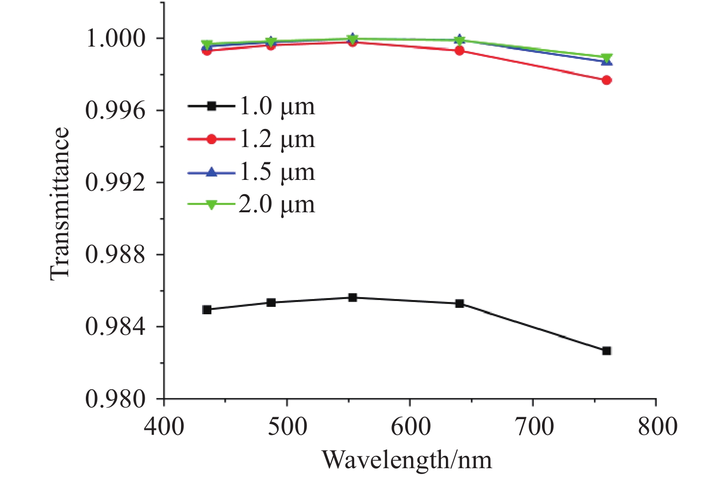
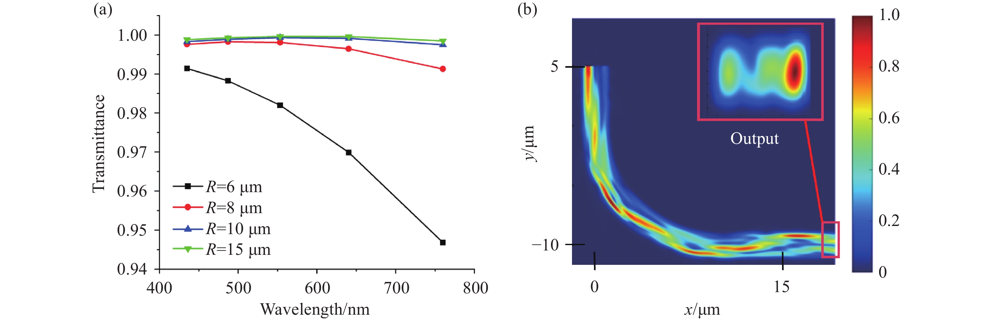
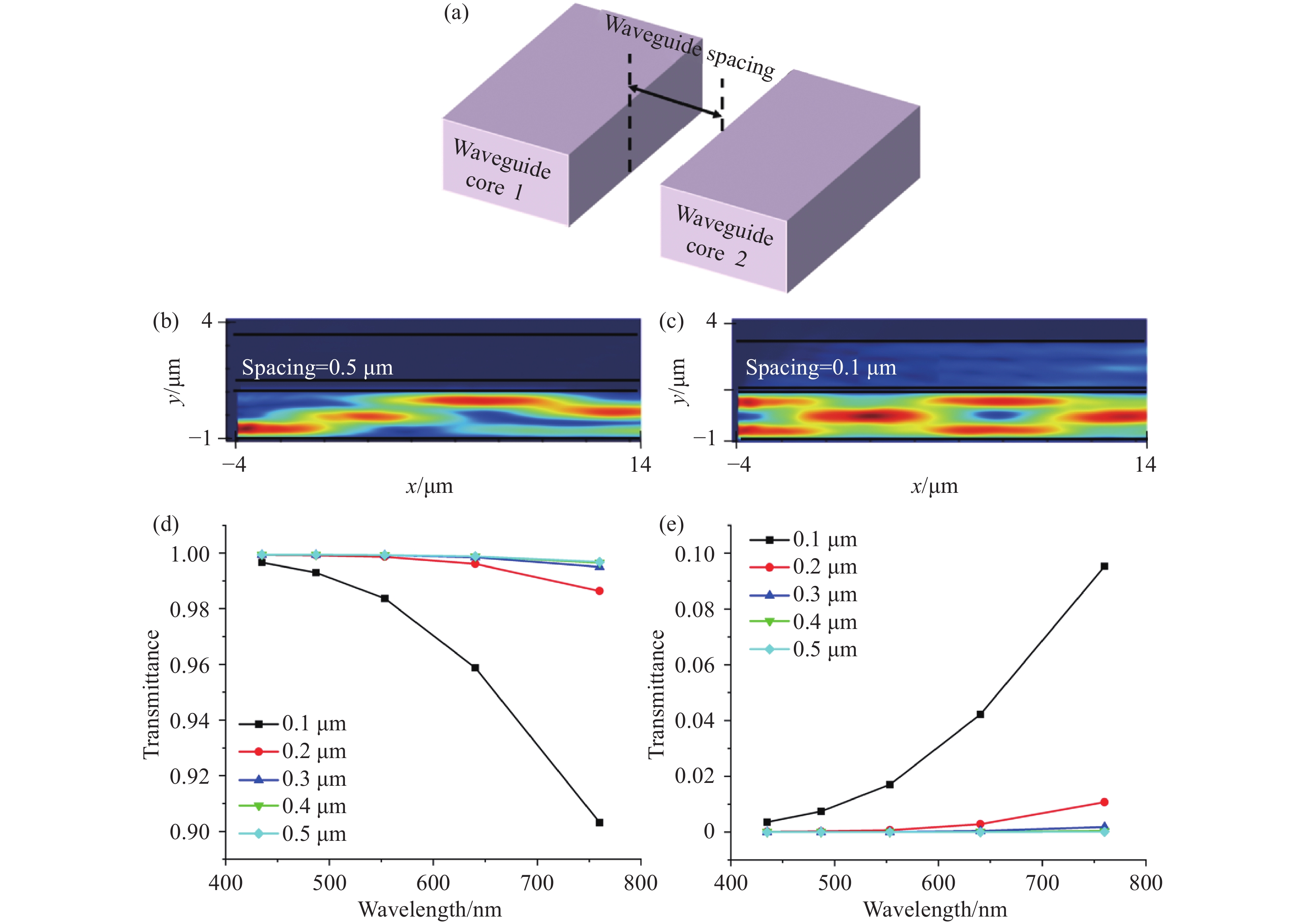
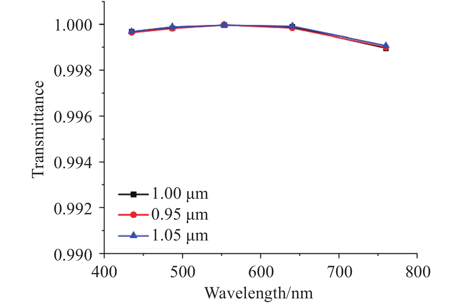
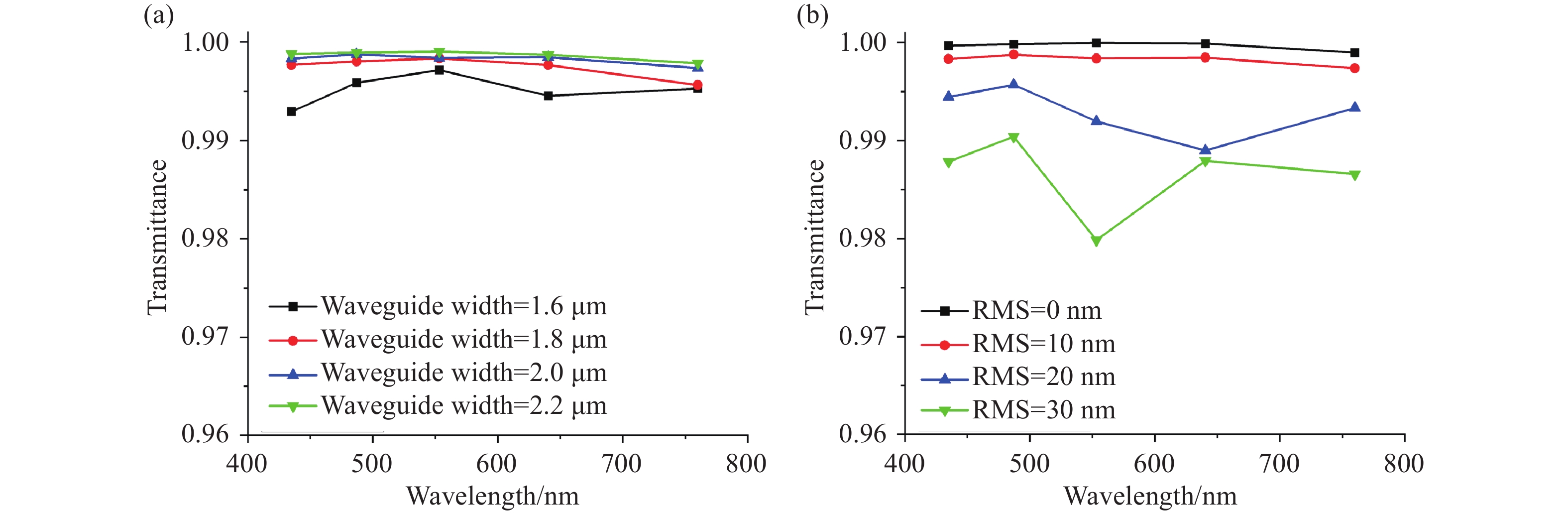
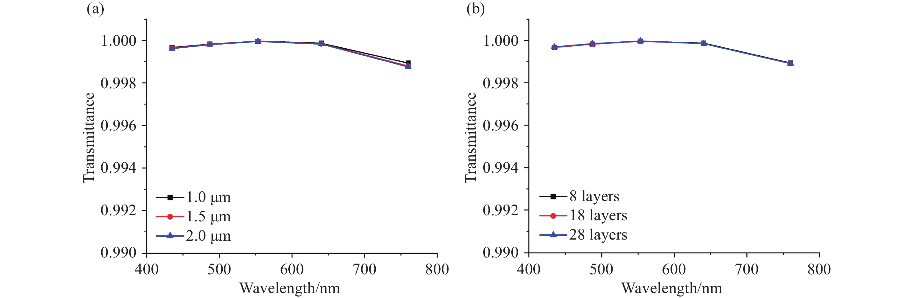
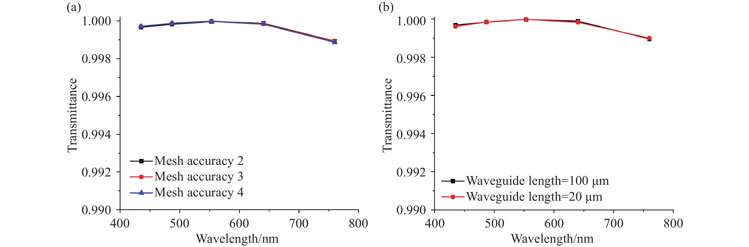
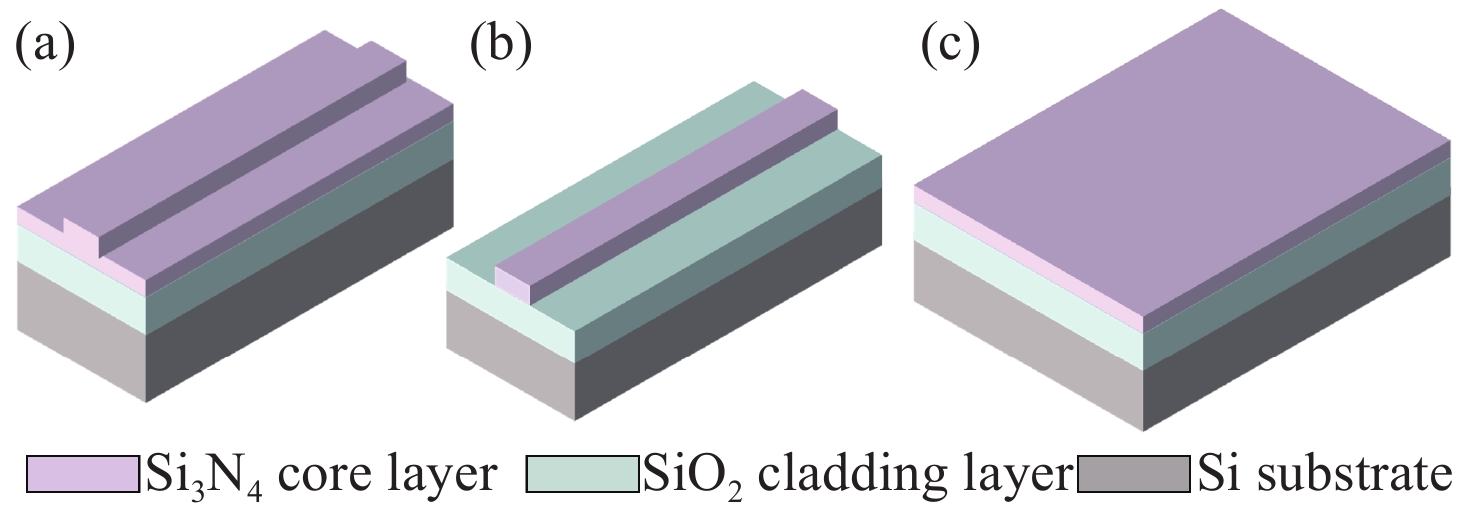
Extending the operational wavelength range of integrated optical devices to cover the entire visible spectrum holds significant importance, as it can enhance the detection accuracy and applicability of miniaturized spectrometers, broaden the bandwidth of visible light communication, and enable biosensors to simultaneously detect multiple biomolecules in complex samples. As the fundamental building block of integrated optical devices, waveguides have not yet been thoroughly investigated for full visible spectrum operation. This work presents a waveguide design supporting the full visible spectrum (435−760 nm). Numerical simulations were employed to analyze the transmission characteristics of various waveguide structures, revealing that single-mode propagation cannot be achieved across the entire visible spectrum. Under multimode propagation conditions, key parameters such as propagation loss and mode distribution were systematically examined to determine the optimal waveguide dimensions, bending radii, and waveguide spacings for low-loss transmission. For slab waveguides, a thickness ≥1 μm ensures polarization insensitivity. For strip waveguides with a thickness of 1 μm, a width ≥2 μm significantly reduces scattering loss induced by sidewall roughness. For strip waveguides with a width of 1 μm and thickness of 2 μm, radiation loss becomes negligible when the bending radius ≥10 μm and waveguide spacing ≥0.4 μm, while maintaining effective isolation from adjacent waveguides. Additionally, the impact of fabrication tolerances on waveguide performance was evaluated. In contrast to previous studies primarily focusing on narrow spectral bands within the visible range, the proposed design enables full visible spectrum transmission in a single waveguide, thereby facilitating bandwidth expansion and performance enhancement for on-chip full visible spectrum devices.

| [1] |
BUTT M A, IMRAN AKCA B, MATEOS X. Integrated photonic biosensors: enabling next-generation lab-on-a-chip platforms[J]. Nanomaterials, 2025, 15(10): 731. doi: 10.3390/nano15100731
|
| [2] |
LIANG W Y, NAN X H, CAI W F, et al. Single-pixel infrared miniaturized spectrometer enabled by ultra-broadband reconfigurable photodetection[J]. Advanced Science, 2025, 12(25): 2500830. doi: 10.1002/advs.202500830
|
| [3] |
WU N F, SUN Y X, HU J T, et al. Intelligent nanophotonics: when machine learning sheds light[J]. eLight, 2025, 5(1): 5. doi: 10.1186/s43593-025-00085-x
|
| [4] |
LIN Y D, YONG ZH, LUO X SH, et al. Monolithically integrated, broadband, high-efficiency silicon nitride-on-silicon waveguide photodetectors in a visible-light integrated photonics platform[J]. Nature Communications, 2022, 13(1): 6362. doi: 10.1038/s41467-022-34100-3
|
| [5] |
CORATO-ZANARELLA M, JI X CH, MOHANTY A, et al. Absorption and scattering limits of silicon nitride integrated photonics in the visible spectrum[J]. Optics Express, 2024, 32(4): 5718-5728. doi: 10.1364/OE.505892
|
| [6] |
CHAUHAN N, WANG J W, BOSE D, et al. Ultra-low loss visible light waveguides for integrated atomic, molecular, and quantum photonics[J]. Optics Express, 2022, 30(5): 6960-6969. doi: 10.1364/OE.448938
|
| [7] |
DUAN L, STEINER T J, PINTUS P, et al. Visible-telecom entangled-photon pair generation with integrated photonics: guidelines and a materials comparison[J]. ACS Photonics, 2025, 12(1): 118-127. doi: 10.1021/acsphotonics.4c01238
|
| [8] |
SIKDER P, RAHMAN M T, BAKIBILLAH A S M. Advancements and challenges of visible light communication in intelligent transportation systems: a comprehensive review[J]. Photonics, 2025, 12(3): 225. doi: 10.3390/photonics12030225
|
| [9] |
HUI ZH Q, LI J Y, LI T T, et al. Study of silicon nitride waveguide-based ultra-wideband on-chip light source for OCT applications[J]. Journal of Infrared and Millimeter Waves, 2024, 43(5): 671-683. (in Chinese). doi: 10.11972/j.issn.1001-9014.2024.05.011
|
| [10] |
POON J K S, GOVDELI A, SHARMA A, et al. Silicon photonics for the visible and near-infrared spectrum[J]. Advances in Optics and Photonics, 2024, 16(1): 1-59. doi: 10.1364/AOP.501846
|
| [11] |
TAO Y SH, TAO Z H, LI L, et al. Silicon integrated microwave photonics[J]. Science China Information Sciences, 2025, 68(4): 140401. doi: 10.1007/s11432-025-4330-y
|
| [12] |
MAMMERI M, HASHEMI B, CRISCI T, et al. Single mode rib waveguide design using machine learning techniques[C]. EPJ Web of Conferences, EDP Sciences, 2024: 01010.
|
| [13] |
AALTO T, CHERCHI M, HARJANNE M, et al. Open-access 3-μm SOI waveguide platform for dense photonic integrated circuits[J]. IEEE Journal of Selected Topics in Quantum Electronics, 2019, 25(5): 8201109.
|
| [14] |
SOREF R A, SCHMIDTCHEN J, PETERMANN K. Large single-mode rib waveguides in GeSi-Si and Si-on-SiO/sub 2/[J]. IEEE Journal of Quantum Electronics, 1991, 27(8): 1971-1974. doi: 10.1109/3.83406
|
| [15] |
HE J J, KOTELES E S, LAMONTAGNE B, et al. Integrated polarization compensator for WDM waveguide demultiplexers[J]. IEEE Photonics Technology Letters, 1999, 11(2): 224-226. doi: 10.1109/68.740711
|
| [16] |
ZHU N. Proposal of a polarization-insensitive echelle grating demultiplexer based on a nanophotonic silicon-on-insulator platform through a dual-grating system[J]. Optics Letters, 2010, 35(10): 1599-1601. doi: 10.1364/OL.35.001599
|
| [17] |
FENG D Z, QIAN W, LIANG H, et al. Fabrication insensitive echelle grating in silicon-on-insulator platform[J]. IEEE Photonics Technology Letters, 2011, 23(5): 284-286.
|
| [18] |
KHURANA M, DELFAN S, YI ZH H. Wafer-scale waveguide sidewall roughness scattering loss characterization by image processing[J]. Optics Express, 2025, 33(10): 20645-20655. doi: 10.1364/OE.558186
|
| [19] |
LAN Y, LIU S W, CHENG CH, et al. Ultra-compact multimode waveguide bends with arbitrary bending angles[J]. Optics Express, 2025, 33(6): 13133-13144. doi: 10.1364/OE.555795
|
| [20] |
YI X G, ZHANG Y B, CHEN Y, et al. On-chip silicon photonic nanohole metamaterials enabled high-density waveguide arrays[J]. Optics Express, 2024, 32(11): 19792-19800. doi: 10.1364/OE.523121
|
| [21] |
CONG Q Y, LI ZH Y, ZHOU J J, et al. Process development of low-loss thick silicon nitride waveguide on 8-inch wafer[J]. Acta Photonica Sinica, 2024, 53(9): 0913002. (in Chinese). doi: 10.3788/gzxb20245309.0913002
|
| [22] |
DUPONT H. Low loss silicon nitride waveguides for photonic integrated circuits[D]. Lausanne: Swiss Federal Institute of Technology, 2019: 1-52.
|
| [23] |
PFEIFFER M H P, KORDTS A, BRASCH V, et al. Photonic damascene process for integrated high-Q microresonator based nonlinear photonics[J]. Optica, 2016, 3(1): 20-25. doi: 10.1364/OPTICA.3.000020
|
| [24] |
GRILLOT F, VIVIEN L, CASSAN E, et al. Influence of waveguide geometry on scattering loss effects in submicron strip silicon-on-insulator waveguides[J]. IET Optoelectronics, 2008, 2(1): 1-5. doi: 10.1049/iet-opt:20070001
|
| [25] |
YAKUHINA A, KADOCHKIN A, SVETUKHIN V, et al. Investigation of side wall roughness effect on optical losses in a multimode Si3N4 waveguide formed on a quartz substrate[J]. Photonics, 2020, 7(4): 104. doi: 10.3390/photonics7040104
|
| [26] |
LIN P T, SINGH V, LIN H Y G, et al. Low-stress silicon nitride platform for mid-infrared broadband and monolithically integrated microphotonics[J]. Advanced Optical Materials, 2013, 1(10): 732-739. doi: 10.1002/adom.201300205
|
Figures(14) / Tables(1)


 DownLoad: