


Reseach progress of bent waveguide and its applications
-
摘要: 本文主要分析了弯曲波导损耗机理,包括传输损耗、辐射损耗、模式转换损耗。重点综述了设计低损耗弯曲波导的方法,包括波导材料、弯曲波导的曲线形状、波导种类、脊型波导的宽度、脊高、弯曲半径、模场分布、弯曲波导曲线形状和其他新型波导结构等。简要概括了近年来设计和制备低损耗弯曲波导的代表性工作。介绍了弯曲波导在集成光学中的应用。通过对弯曲波导的损耗及耦合机制理论的不断完善,实现光在较小弯曲半径的低损耗传输,从而提高集成光学的集成度是弯曲波导今后的发展趋势。Abstract: The loss mechanism of bent waveguide including the bending loss, propagation loss, radiation loss and the loss of mode conversion are theorically analysed in this paper. It focuses on the review of the design of low loss bent waveguide, including materials, the shape of bent waveguide, strip or rib waveguide, the width, height and radius of the bent waveguide, the dismatch of mode, the shape of the curve and other new structures. The representative works on the design and fabrication of low loss bent waveguides are summarized. The development status of the low loss bent waveguide is analysed and its applications in integrated optical are introduced. The future developing trend of bent waveguide is to develope the theory of the loss characterization and wave coupling, and to realize low bending loss with very small bending radii for high desity integration in Photonics Integrated Circuits (PICs).
-
Key words:
- bent waveguide /
- integrated optical /
- Silicon-on-insulator (SOI) /
- low-loss-waveguide
-

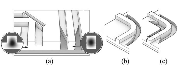
图 1 (a) TIR形弯曲波导的单模脊形波导,弯曲部分损耗0.3 dB/90°。也可以通过低损耗的锥形转换器与矩形波导相连接。(b) 带有沟槽部分的90°弯曲脊形波导。(c) 优化后的多模弯曲波导,从而减少弯曲波导尺寸和损耗[67]
Figure 1. Micron-scale silicon photonics platform. (a) single mode rib waveguides can be tightly bent by TIR mirrors with 0.3 dB/90° loss; they can be also be turned into strip waveguides by almost lossless converters; (b) a 90° ridge waveguide bend with a groove structure; (c) suitably designed bends of multimode strip waveguides to dramatically reduce bend size and losses[67]


-
[1] CHEN R, NG K W, KO W S, et al.. Nanophotonic integrated circuits from nanoresonators grown on silicon[J]. Nature Communications, 2014, 5:1-9. https://www.researchgate.net/publication/263708999_Nanophotonic_integrated_circuits_from_nanoresonators_grown_on_silicon [2] DAI D, WU H, GUAN X. SOI (Silicon-on-insulator)-compatible hybrid nanoplasmonics:waveguiding, polarization-handling, and thermal-tuning[J]. Nanophotonics and Micro/Nano Optics Ⅱ, 2014:9277. [3] DAI D X, BAUTERS J, BOWERS J E. Passive technologies for future large-scale photonic integrated circuits on silicon:polarization handling, light non-reciprocity and loss reduction[J]. Light-Sci. Appl., 2012, 1:12. doi: 10.1038/lsa.2012.12 [4] BOEUF F, CREMER S, VULLIET N, et al.. A multi-wavelength 3D-compatible silicon photonics platform on 300 mm SOI wafers for 25 Gb/s applications[C]. IEDM, 2013:13.13.11-13.13.14. [5] WELCH DF, KISH FA, MELLE S, et al.. Large-Scale InP photonic integrated circuits:enabling efficient scaling of optical transport networks[J]. IEEE J. Selected Topics in Quantum Electronics, 2007, 13(1):22-31. doi: 10.1109/JSTQE.2006.890068 [6] NICHOLES S C, MASANOVIC M L, JEVREMOVIC B, et al.. An 88 InP Monolithic Tunable Optical Router (MOTOR) packet forwarding chip[J]. J. Lightwave Technology, 2010, 28(4):641-650. doi: 10.1109/JLT.2009.2030145 [7] TAYLOR H F. Power loss at directional change in dielectric waveguides[J]. Applied Optics, 1974, 13(3):642-647. doi: 10.1364/AO.13.000642 [8] LADOUCEUR F, LABEYE P. A new general-approach to optical wave-guide path design[J]. J. Lightwave Technology, 1995, 13(3):481-492. doi: 10.1109/50.372446 [9] SUBBARAMAN H, XU X, HOSSEINI A, et al.. Recent advances in silicon-based passive and active optical interconnects[J]. Optics Express, 2015, 23(3):2487-2510. doi: 10.1364/OE.23.002487 [10] SMIT M K. InP photonic integrated circuits[J]. IEEE J. Selected Topics in Quantum Electronics, 2002, 16(5):1113-1125. [11] KAWACHI M. Recent progress in silica-based planar lightwave circuits on silicon[J]. Optoelectronics, IEE Proceedings, 1996, 143(5):257-262. doi: 10.1049/ip-opt:19960493 [12] ZHANG X, HOSSEINI A, LIN X, et al.. Polymer-based hybrid integrated photonic devices for silicon on-chip modulation and board-level optical interconnects[J]. IEEE J. Selected Topics in Quantum Electronics, 2014, 19(6):3401115. http://www.oalib.com/paper/3579041 [13] LEE H, CHEN T, LI J, et al.. Ultra-low-loss optical delay line on a silicon chip[J]. Nature Communications, 2012, 3:7. [14] BAUTERS J F, HECK M J R, JOHN D, et al.. Ultra-low-loss high-aspect-ratio Si3N4 waveguides[J]. Optics Express, 2011, 19(4):3163-3174. doi: 10.1364/OE.19.003163 [15] BAUTERS J F, HECK M J, JOHN D D, et al. Planar waveguides with less than 0.1 dB/m propagation loss fabricated with wafer bonding[J]. Optics Express, 2011, 19(24):24090-24101. doi: 10.1364/OE.19.024090 [16] ADAR R, SERBIN M R, MIZRAHI V. Less than 1 dB per meter propagation loss of silica wave-guides measured using a ring resonator[J]. J. Lightwave Technology, 1994, 12(8):1369-1372. doi: 10.1109/50.317523 [17] KOBAYASHI N, SATO K, NAMIWAKA M, et al.. Silicon photonic hybrid ring-filter external cavity wavelength tunable lasers[J]. J. Lightwave Technology, 2015, 33(6):1241-1246. doi: 10.1109/JLT.2014.2385106 [18] SOREF R A, LARENZO J. All-silicon active and passive guided-wave components for λ=1.3 and 1.6μm[J]. IEEE J. Quantum Electronics, 1986, 22(6):873-879. doi: 10.1109/JQE.1986.1073057 [19] SOREF R A. Silicon-based optoelectronics[J]. Proceedings of the IEEE, 1994, 23(12):1687-1706. [20] JALALI B, TRINH P D, YEGNANARAYANAN S, et al.. Guided-wave optics in silicon-on-insulator technology[J]. IEE Proceedings-optoelectronics, 1996, 143(5):307-311. doi: 10.1049/ip-opt:19960675 [21] JALALI B, YEGNANARAYANAN S, YOON T, et al.. Advances in silicon-on-insulator optoelectronics[J]. IEEE J. Selected Topics in Quantum Electronics, 1998, 4(6):938-947. doi: 10.1109/2944.736081 [22] LIBERTINO S, COFFA S, SAGGIO M. Design and fabrication of integrated Si-based optoelectronic devices[J]. Materials Science in Semiconductor Processing, 2000, 3(5):375-381. https://www.researchgate.net/publication/222689342_Design_and_fabrication_of_integrated_Si-based_optoelectronic_devices [23] VLASOV Y A, MCNAB S J. Losses in single-mode silicon-on-insulator strip waveguides and bends[J]. Optics Express, 2004, 12(8):1622-1631. doi: 10.1364/OPEX.12.001622 [24] YONGBO T, HUI-WEN C, SIDDHARTH J, et al.. 50 Gb/s hybrid silicon traveling-wave electroabsorption modulator[J]. Optics Express, 2011, 19(7):5811-5816. doi: 10.1364/OE.19.005811 [25] QIANFAN X, BRADLEY S, SAMEER P, et al. Micrometre-scale silicon electro-optic modulator[J]. Nature, 2005, 435(7040):325-327. doi: 10.1038/nature03569 [26] JONES R, LIU A S, RONG H S, et al.. Lossless optical modulation in a silicon waveguide using stimulated Raman scattering[J]. Optics Express, 2005, 13(5):1716-1723. doi: 10.1364/OPEX.13.001716 [27] LIU A S, JONES R, LIAO L, et al.. A high-speed silicon optical modulator based on a metal-oxide-semiconductor capacitor[J]. Nature, 2004, 427(6975):615-618. doi: 10.1038/nature02310 [28] RICKMAN A G, REED G T, NAMAVAR F. Silicon-on-insulator optical rib waveguide loss and mode characteristics[J]. J. Lightwave Technology, 1994, 12(10):1771-1776. doi: 10.1109/50.337489 [29] MELLONI A, CARNIEL F, COSTA R, et al. Determination of bend mode characteristics in dielectric waveguides[J]. J. Lightwave Technology, 2001, 19(4):571-577. doi: 10.1109/50.920856 [30] SINGH A. Influence of carrier transport on Raman amplification in silicon waveguides[J]. Optics Express, 2010, 18(12):12569-12580. doi: 10.1364/OE.18.012569 [31] RICARDO C, RAGHUNATHAN V, DIMITROPOULOS D, et al. Influence of nonlinear absorption on Raman amplification in Silicon waveguides[J]. Optics Express, 2004, 12(12):2774-2780. doi: 10.1364/OPEX.12.002774 [32] DIMITROPOULOS D, FATHPOUR S, JALALI B. Limitations of active carrier removal in silicon Raman amplifiers and lasers[J]. Applied Physics Letters, 2005, 87(26):261108-3. doi: 10.1063/1.2155071 [33] LIU Y, TSANG H K. Nonlinear absorption and Raman gain in helium-ion-implanted silicon waveguides[J]. Optics Letters, 2006, 31(11):1714-1716. doi: 10.1364/OL.31.001714 [34] HEWITT P D, REED G T. Improving the response of optical phase modulators in SOI by computer simulation[J]. J. Lightwave Technology, 2000, 18(3):443-450. doi: 10.1109/50.827519 [35] GRILLOT F, VIVIEN L, CASSAN E, et al.. Influence of waveguide geometry on scattering loss effects in submicron strip silicon-on-insulator waveguides[J]. IET Optoelectronics, 2008, 2(1):1-5. doi: 10.1049/iet-opt:20070001 [36] PAYNE F P, LACEY J P R. A theoretical analysis of scattering loss from planar optical waveguides[J]. Optical & Quantum Electronics, 1994, 26(10):977-986. [37] PAFCHEK R, TUMMIDI R, LI J, et al.. Low-loss silicon-on-insulator shallow-ridge TE and TM waveguides formed using thermal oxidation[J]. Applied Optics, 2009, 48(5):958-963. doi: 10.1364/AO.48.000958 [38] LEE K K, LIM D R, KIMERLING L C, et al.. Fabrication of ultralow-loss Si/SiO2 waveguides by roughness reduction[J]. Optics Letters, 2001, 26(23):1888-1890. doi: 10.1364/OL.26.001888 [39] LIU H C, LIN Y H, HSU W. Sidewall roughness control in advanced silicon etch process[J]. Microsystem Technologies, 2003, 10(1):29-34. doi: 10.1007/s00542-003-0309-8 [40] GAO F, WANG Y, CAO G, et al.. Improvement of sidewall surface roughness in silicon-on-insulator rib waveguides[J]. Applied Physics B, 2005, 81(5):691-694. doi: 10.1007/s00340-005-1951-x [41] CHABLOZ M, SAKAI Y, MATSUURA T, et al. Improvement of sidewall roughness in deep silicon etching[J]. Microsystem Technologies, 2000, 6(3):86-89. doi: 10.1007/s005420050003 [42] SNYDER A W. Radiation losses due to variations of radius on dielectric or optical fibers[J]. IEEE Transactions on Microwave Theory and Techniques, 1970, 18(9):608-614. doi: 10.1109/TMTT.1970.1127296 [43] LEWIN L. Radiation from curved dielectric slabs and fibers[J]. IEEE Transactions on Microwave Theory & Techniques, 1974, 22(7):718-727. [44] KUESTER E F, CHANG D C. Surface-wave radiation loss from curved dielectric slabs and fibers[J]. IEEE J. Quantum Electronics, 1975, 11(11):903-907. doi: 10.1109/JQE.1975.1068548 [45] MARCUSE D. Curvature loss formula for optical fibers[J]. J. Optical Society of America, 1976, 66(3):216-220. doi: 10.1364/JOSA.66.000216 [46] MIYAGI M, NISHIDA S. Bending losses of dielectric rectangular waveguides for integrated optics[J]. J. Optical Society of America, 1978, 68(68):316-319. https://www.researchgate.net/publication/243755215_Bending_losses_of_dielectric_rectangular_waveguides_for_integrated_optics [47] WHITE I A. Radiation from bends in optical waveguides:the volume-current method[J]. IEEE J. Microwaves, 1979, 3(5):186-188. doi: 10.1049/ij-moa.1979.0043 [48] COLLIN R. Field Theory of Guided Waves[M]. McGraw-Hill, 1960. [49] BRIMONT A, HU X, CUEFF S, et al.. Low-loss and compact silicon rib waveguide bends[J]. IEEE Photonics Technology Letters, 2016, 28(3):299-302. doi: 10.1109/LPT.2015.2495230 [50] MITOMI O, KASAYA K, MIYAZAWA H. Design of a single-mode tapered waveguide for low-loss chip-to-fiber coupling[J]. IEEE J. Quantum Electronics, 1994, 30(8):1787-1793. doi: 10.1109/3.301643 [51] ALMEIDA V R, PANEPUCCI R R, MICHAL L. Nanotaper for compact mode conversion[J]. Optics Letters, 2003, 28(15):1302-1304. doi: 10.1364/OL.28.001302 [52] MARCATILI E A J. Bends in optical dielectric guides[J]. Bell System Technical Journal, 1969, 48(7):2103-2132. doi: 10.1002/bltj.1969.48.issue-7 [53] HEIBLUM M, HARRIS J H. Analysis of curved optical-waveguides by conformal transformation[J]. IEEE J. Quantum Electronics, 1975, 11(2):75-83. doi: 10.1109/JQE.1975.1068563 [54] CHILWELL J, HODGKINSON I. Thin-films field-transfer matrix theory of planar multilayer waveguides and reflection from prism-loaded waveguides[J]. J. Optical Society of America A Optics & Image Science, 1984, 1(7):742-753. https://www.researchgate.net/publication/239007421_Thin-films_field-transfer_matrix_theory_of_planar_multilayer_waveguides_and_reflection_from_prism-loaded_waveguides [55] THYAGARAJAN K, RAMADAS M R, SHENOY M R. Beat-length measurement of birefringent optical fibers[J]. Optics Letters, 1987, 12(11):935-937. doi: 10.1364/OL.12.000935 [56] DAI D X, SAILING H. Analysis of characteristics of bent rib waveguides[J]. J. Optical Society of America A Optics Image Science & Vision, 2004, 21(1):113-121. [57] YAMAMOTO T, KOSHIBA M. Numerical analysis of curvature loss in optical waveguides by the finite-element method[J]. J. Lightwave Technology, 1993, 11(10):1579-1583. doi: 10.1109/50.249899 [58] GU J S, BESSE P A, MELCHIOR H. Method of lines for the analysis of the propagation characteristics of curved optical rib waveguides[J]. IEEE J. Quantum Electronics, 1991, 27(3):531-537. [59] FENG N N, ZHOU G R, XU C, et al.. Computation of full-vector modes for bending waveguide using cylindrical perfectly matched layers[J]. J. Lightwave Technology, 2002, 20(11):1976-1980. doi: 10.1109/JLT.2002.806333 [60] DAI D X, SHI Y C. Deeply etched SiO2 ridge waveguide for sharp bends[J]. J. Lightwave Technology, 2006, 24(12):5019-5024. doi: 10.1109/JLT.2006.885243 [61] HU Z, LU Y Y. Computing optimal waveguide bends with constant width[J]. J. Lightwave Technology, 2007, 25(10):3161-3167. doi: 10.1109/JLT.2007.904033 [62] CHERCHI M, YLINEN S, HARJANNE M, et al.. Low-loss spiral waveguides with ultra-small footprint on a micron scale SOI platform[J]. Silicon Photonics Ix, 2014, 8990. [63] ZHUANG L M, MARPAUNG D, BURLA M, et al.. Low-loss, high-index-contrast Si3N4/SiO2 optical waveguides for optical delay lines in microwave photonics signal processing[J]. Optics Express, 2011, 19(23):23162-23170. doi: 10.1364/OE.19.023162 [64] HU R, DAI D, HE S. A small polymeric ridge waveguide with a high index contrast[J]. J. Lightwave Technology, 2008, 26(13-16):1964-1968. https://www.researchgate.net/publication/3244617_A_Small_Polymeric_Ridge_Waveguide_With_a_High_Index_Contrast [65] FISCHER U, ZINKE T, KROPP J R, et al.. 0.1 dB/cm waveguide losses in single-mode SOI rib waveguides[J]. IEEE Photonics Technology Letters, 1996, 8(5):647-648. doi: 10.1109/68.491567 [66] TANG Y Z, WANG W H, LI T, et al. Integrated waveguide turning mirror in silicon-on-insulator[J]. Photonics Technology Letters IEEE, 2002, 14(1):68-70. doi: 10.1109/68.974164 [67] CHERCHI M, YLINEN S, HARJANNE M, et al.. Dramatic size reduction of waveguide bends on a micron-scale silicon photonic platform[J]. Optics Express, 2013, 21(15):17814-17823. doi: 10.1364/OE.21.017814 [68] ERIC D, FENGNIAN X, LAURENT S, et al.. Group index and group velocity dispersion in silicon-on-insulator photonic wires[J]. Optics Express, 2006, 14(9):3853-3863. doi: 10.1364/OE.14.003853 [69] MUSA S, BORREMAN A, KOK A A M, et al.. Experimental study of bent multimode optical waveguides[J]. Annals of Surgery,1984, 200(2):153-158. doi: 10.1097/00000658-198408000-00006 [70] HARJANNE M, AALTO T. Design of tight bends in silicon-on-insulator ridge waveguides[J]. Physica Scripta, 2004, T114:209-212. doi: 10.1088/0031-8949/2004/T114/053 [71] AALTO T, CHERCHI M, HARJANNE M, et al.. Launching of multi-project wafer runs in ePIXfab with micron-scale silicon rib waveguide technology[J]. Silicon Photonics Ⅸ, 2014, 8990. [72] SOLEHMAINEN K, AALTO T, DEKKER J, et al. Development of multi-step processing in silicon-on-insulator for optical waveguide applications[J]. J. Optics a-Pure and Applied Optics, 2006, 8(7):S455-S460. doi: 10.1088/1464-4258/8/7/S22 [73] SOREF R A, SCHMIDTCHEN J, PETERMANN K. Large single-mode rib waveguides in GeSi-Si and Si-on-SiO2[J]. Quantum Electronics IEEE J., 1991, 27(8):1971-1974. doi: 10.1109/3.83406 [74] DULLO F T, TINGUELY J C, SOLBO S A, et al.. Single-mode limit and bending losses for shallow rib Si3N4 waveguides[J]. IEEE Photonics J., 2015, 7(1):2700511-10. https://www.researchgate.net/profile/Stian_Solbo/publication/273166722_Single-Mode_Limit_and_Bending_Losses_for_Shallow_Rib_Si3N4_Waveguides/links/552cdea60cf2e089a3acfc02.pdf?origin=publication_detail [75] DAY I E, EVANS I, KNIGHTS A, et al.. Tapered silicon waveguides for low insertion loss highly-efficient high-speed electronic variable optical attenuators[C]. Optical Fiber Communications Conference, 2003. OFC 2003, 2003:249-251. [76] ANITA S, THOMAS D, JANUSZ M, et al.. Fabrication and characterization of three-dimensional silicon tapers[J]. Optics Express, 2003, 11(26):3555-3561. doi: 10.1364/OE.11.003555 [77] SMIT M K, PENNINGS E C M, BLOK B. Normalized approach to the design of low-loss optical waveguide bends[J]. J. Lightwave Technology, 1993, 11(11):1737-1742. doi: 10.1109/50.251169 [78] NGUYEN T G, TUMMIDI R S, KOCH T L, et al.. Lateral leakage of TM-like mode in thin-ridge silicon-on-insulator bent waveguides and ring resonators[J]. Optics Express, 2010, 18(7):7243-7252. doi: 10.1364/OE.18.007243 [79] ZHANG X M, HARRISON M, HARKER A, et al.. Serpentine low loss trapezoidal silica waveguides on silicon[J]. Optics Express, 2012, 20(20):22298-22307. doi: 10.1364/OE.20.022298 [80] MANOLATOU C, JOHNSON S G, FAN S, et al. High-density integrated optics[J]. J. Lightwave Technology, 1999, 17(9):1682-1692. doi: 10.1109/50.788575 [81] HOCHBERG M, BAEHRJONES T. Towards fabless silicon photonics[J]. Nature Photonics, 2010, 4(8):492-494. doi: 10.1038/nphoton.2010.172 [82] PO D, WEI Q, HONG L, et al.. Low power and compact reconfigurable multiplexing devices based on silicon microring resonators[J]. Optics Express, 2010, 18(10):9852-9858. doi: 10.1364/OE.18.009852 [83] NEUMANN E G. Curved Dielectric Optical Waveguide with Reduced Transition Losses[J]. Microwaves Antennas & Propagation, 1982, 129(5):278-280. [84] SMIT M K, PENNINGS E C M, BLOK H. A normalized approach to the design of low-loss optical wave-guide bends[J]. J. Lightwave Technology, 1993, 11(11):1737-1742. doi: 10.1109/50.251169 [85] PENNINGS E C M. Bends in optical ridge waveguides:modeling and experiments[D]. Netherland:Delft University of Technology, 1990. [86] FAN G, SANG W, LIU X, et al.. Silicon waveguide racetrack resonators with 1.5μm radius using junction offsets[J]. Microwave & Optical Technology Letters, 2012, 54(6):1470-1471. [87] CHEN T, LEE H, LI J, et al. A general design algorithm for low optical loss adiabatic connections in waveguides[J]. Optics Express, 2012, 20(20):22819-22829. doi: 10.1364/OE.20.022819 [88] CAI D P, LU J H, CHEN C C, et al. High Q-factor microring resonator wrapped by the curved waveguide[J]. Scientific Reports, 2015, 5. https://www.researchgate.net/publication/277084453_High_Q-factor_microring_resonator_wrapped_by_the_curved_waveguide [89] LAI C H, CHANG T, YEH Y S. Characteristics of bent terahertz antiresonant reflecting pipe waveguides[J]. Optics Express, 2014, 22(7):8460-8472. doi: 10.1364/OE.22.008460 [90] MELLONI A, MONGUZZI P, COSTA R, et al.. Design of curved waveguides:the matched bend[J]. J. Optical Society of America a-Optics Image Science and Vision, 2003, 20(1):130-137. doi: 10.1364/JOSAA.20.000130 [91] YUAN W, HALL D C. A General Scaling Rule for Matched Bend Waveguides[J]. J. Lightwave Technology, 2011, 29(24):3786-3796. doi: 10.1109/JLT.2011.2174335 [92] YUAN W, SEIBERT C S, HALL D C. Single-facet teardrop laser with matched-bends design[J]. IEEE J. Selected Topics in Quantum Electronics, 2011, 17(6):1662-1669. doi: 10.1109/JSTQE.2011.2111360 [93] LEE H, CHEN T, LI J, et al.. Chemically etched ultrahigh-Q wedge-resonator on a silicon chip[J]. Nature Photonics, 2012, 6(6):369-373. doi: 10.1038/nphoton.2012.109 [94] CHEN T, LEE H, VAHALA K J. Design and characterization of whispering-gallery spiral waveguides[J]. Optics Express, 2014, 22(5):5196-5208. doi: 10.1364/OE.22.005196 [95] SHEEHAN R N, HORNE S, PETERS F H. The design of low-loss curved waveguides[J]. Optical and Quantum Electronics, 2008, 40(14-15):1211-1218. doi: 10.1007/s11082-009-9329-7 [96] BAETS R, LAGASSE P E. Loss calculation and design of arbitrarily curved integrated-optic waveduides[J]. J. Optical Society of America, 1983, 73(2):177-182. doi: 10.1364/JOSA.73.000177 [97] DAI D X. Multimode optical waveguide enabling microbends with low inter-mode crosstalk for mode-multiplexed optical interconnects[J]. Optics Express, 2014, 22(22):27524-27534. doi: 10.1364/OE.22.027524 [98] KRAUSE M, RENNER H, BRINKMEYER E. Polarization-dependent curvature loss in silicon rib waveguides[J]. IEEE J. Selected Topics in Quantum Electronics, 2006, 12(6):1359-1362. doi: 10.1109/JSTQE.2006.884068 [99] DAOXIN D, BOWERS J E. Novel concept for ultracompact polarization splitter-rotator based on silicon nanowires[J]. Optics Express, 2011, 19(11):10940-10949. doi: 10.1364/OE.19.010940 [100] VERMEULEN D, ACOLEYEN K V, GHOSH S, et al.. Efficient tapering to the fundamental quasi-TM mode in asymmetrical waveguides[C]. 15th European conference on Integrated Optics (ECIO 2010), 2010. [101] CHERCHI M, YLINEN S, HARJANNE M, et al.. The Euler bend:paving the way for high-density integration on micron-scale semiconductor platforms[J]. Silicon Photonics Ix, 2014, 8990. http://proceedings.spiedigitallibrary.org/pdfaccess.ashx?url=/data/conferences/spiep/78713/899004.pdf [102] MEKIS A, CHEN J C, KURLAND I I, et al.. High transmission through sharp bends in photonic crystal waveguides[J]. Physical Review Letters, 1996, 77(18):3787-3790. doi: 10.1103/PhysRevLett.77.3787 [103] BOGAERTS W, BAETS R, DUMON P, et al. Nanophotonic waveguides in silicon-on-insulator fabricated with CMOS technology[J]. J. Lightwave Technology, 2005, 23(1):401-412. doi: 10.1109/JLT.2004.834471 [104] ALMEIDA V R, QIANFAN X, BARRIOS C A, et al.. Guiding and confining light in void nanostructure[J]. Optics Letters, 2004, 29(11):1209-1211. doi: 10.1364/OL.29.001209 [105] KOOS C, VORREAU P, VALLAITIS T, et al.. All-optical high-speed signal processing with silicon-organic hybrid slot waveguides[J]. Nature Photonics, 2009, 3(4):216-219. doi: 10.1038/nphoton.2009.25 [106] JUNG E J, LEE W J, KIM M J, et al.. Design of hybrid optical waveguide with a 90A degrees bend structure for high density photonics integrated circuits[J]. Optical and Quantum Electronics, 2013, 45(7):721-726. doi: 10.1007/s11082-012-9633-5 [107] CLAUDIO D, THEO L, MARTIN O J F, et al.. Simulation of complex plasmonic circuits including bends[J]. Optics Express, 2011, 19(20):18979-18988. doi: 10.1364/OE.19.018979 [108] 管小伟, 吴昊, 戴道锌.硅基混合表面等离子体纳米光波导及集成器件[J].中国光学, 2014, (2):181-195. http://www.chineseoptics.net.cn/CN/abstract/abstract9117.shtmlGUAN X W, WU H, DAI D X. Silicon hybrid surface plasmonic nano-optics-waveguide and integration devices[J]. Chinese Optics, 2014, (2):181-195. http://www.chineseoptics.net.cn/CN/abstract/abstract9117.shtml [109] ZHOU X, ZHANG T, CHEN L, et al.. A Graphene-based hybrid plasmonic waveguide with ultra-deep subwavelength confinement[J]. J. Lightwave Technology, 2014, 32(21):4199-4203. doi: 10.1109/JLT.2014.2350487 [110] DAOXIN D, SAILING H. A silicon-based hybrid plasmonic waveguide with a metal cap for a nano-scale light confinement[J]. Optics Express, 2009, 17(19):16646-16653. doi: 10.1364/OE.17.016646 [111] CHEN P X, ZHU Y P, SHI Y C, et al.. Fabrication and characterization of suspended SiO2 ridge optical waveguides and the devices[J]. Optics Express, 2012, 20(20):22531-22536. doi: 10.1364/OE.20.022531 [112] LI L X, NORDIN G P, ENGLISH J M, et al.. Integrated Optics:Devices, Materials, and Technologies Ⅶ[M]. SPIE, 2003. [113] CASSAN E, VIVIEN L, LAVAL S. Polarization-independent 90 degrees-turns in single-mode micro-waveguides on silicon-on-insulator wafers for telecommunication wavelengths[J]. Optics Communications, 2004, 235(1-3):83-88. doi: 10.1016/j.optcom.2004.02.080 [114] QIAN Y, KIM S, SONG J, et al.. Compact and low loss silicon-on-insulator rib waveguide 90 degrees bend[J]. Optics Express, 2006, 14(13):6020-6028. doi: 10.1364/OE.14.006020 [115] XIAO S J, KHAN M H, SHEN H, et all. Modeling and measurement of losses in silicon-on-insulator resonators and bends[J]. Optics Express, 2007, 15(17):10553-10561. doi: 10.1364/OE.15.010553 [116] DAI DX. Subwavelength silica-based optical waveguide with a multilayered buffer for sharp bending[J]. Jl Lightwave Technology, 2009, 27(13):2489-2494. doi: 10.1109/JLT.2008.2011501 [117] LUO J, XU P, CHEN H, et al. Realizing almost perfect bending waveguides with anisotropic epsilon-near-zero metamaterials[J]. Applied Physics Letters, 2012, 100(22):221903-221903-221905. doi: 10.1063/1.4723844 [118] FU Y, XU Y, CHEN H. Applications of gradient index metamaterials in waveguides[J]. Scientific Reports, 2015, 5. https://www.researchgate.net/publication/286982878_Applications_of_gradient_index_metamaterials_in_waveguides/fulltext/56953d3708aeab58a9a4d7d0/286982878_Applications_of_gradient_index_metamaterials_in_waveguides.pdf [119] 李浩, 宋玲玲, 张立钧等.4通道交叉型二氧化硅光波导延迟线阵列的设计与制备[J].中国光学, 2014, (3):435-441. http://www.chineseoptics.net.cn/CN/abstract/abstract9143.shtmlLI H, SONG L L, ZHANG L J, et al.. Design and fabrication of 4 channels silica cross optical waveguide delay line array[J]. Chinese Optics, 2014, (3):435-441. http://www.chineseoptics.net.cn/CN/abstract/abstract9143.shtml [120] RASRAS M S, MADSEN C K, CAPPUZZO M A, et al.. Integrated resonance-enhanced variable optical delay lines[J]. IEEE Photonics Technology Letters, 2005, 17(4):834-836. doi: 10.1109/LPT.2005.844009 [121] DENSMORE A, XU D X, JANZ S, et al.. Spiral-path high-sensitive silicon photonic wire molecular sensor with temperature-independent response[J]. Optics Letters, 2008, 33(6):596-598. doi: 10.1364/OL.33.000596 [122] CIMINELLI C, DELLOLIO F, ARMENISE M N. High-Q spiral resonator for optical gyroscope applications:numerical and experimental investigation[J]. IEEE Photonics J., 2012, 4(4):1844-1854. https://www.researchgate.net/publication/233979298_High-Q_Spiral_Resonator_for_Optical_Gyroscope_Applications_Numerical_and_Experimental_Investigation [123] CHAN H P, CHENG S Y, CHUNG P S. Low loss wide-angle symmetric Y-branch waveguide[J]. Electronics Letters, 1996, 32(7):652-654. doi: 10.1049/el:19960452 [124] QIAN W, JUN L, SAILING H. Optimal design method of a low-loss broadband Y branch with a multimode waveguide section[J]. Applied Optics, 2003, 41(36):7644-7649. https://www.researchgate.net/publication/10965541_Optimal_design_method_of_a_low-loss_broadband_Y_branch_with_a_multimode_waveguide_section [125] CHERCHI M, YLINEN S, HARJANNE M, et al.. Fabrication-tolerant optical filters for dense integration on a micron-scale SOI platform[J]. Silicon Photonics Ⅸ, 2014:8990. https://www.researchgate.net/publication/262982534_Fabrication-tolerant_optical_filters_for_dense_integration_on_a_micron-scale_SOI_platform [126] XIAO S J, KHAN M H, SHEN H, et al.. Compact silicon microring resonators with ultra-low propagation loss in the C band[J]. Optics Express, 2007, 15(22):14467-14475. doi: 10.1364/OE.15.014467 [127] XIAO S, KHAN M H, SHEN H, et al.. Silicon-on-insulator microring add-drop filters with free spectral ranges over 30 nm[J]. J. Lightwave Technology, 2008, 26(2):228-236. doi: 10.1109/JLT.2007.911098 [128] LI X B, DENG Q Z, ZHOU Z P. Low loss, high-speed single-mode half-disk resonator[J]. Optics Letters, 2014, 39(13):3810-3813. doi: 10.1364/OL.39.003810 [129] BIAN Z X, LIU B, SHAKOURI A. InP-based passive ring-resonator-coupled lasers[J]. IEEE J. Quantum Electronics, 2003, 39(7):859-865. doi: 10.1109/JQE.2003.813222 [130] KIM K C, HAN I K, LEE J I, et al.. High power single-lateral-mode operation of InAs quantum dot based ridge type laser diodes by utilizing a double bend waveguide structure[J]. Applied Physics Letters, 2010, 96(26):261103-261106. doi: 10.1063/1.3458704 [131] FAUGERON M, VILERA M, KRAKOWSKI M, et al.. High power three-section integrated master oscillator power amplifier at 1.5μm[J]. IEEE Photonics Technology Letters, 2015, 27(13):1449-1452. doi: 10.1109/LPT.2015.2425534 [132] GUAN X, WU H, SHI Y, et al.. Extremely small polarization beam splitter based on a multimode interference coupler with a silicon hybrid plasmonic waveguide[J]. Optics Letters, 2014, 39(2):259-262. doi: 10.1364/OL.39.000259 [133] UEMATSU T, KITAYAMA T, ISHIZAKA Y, et al.. Ultra-broadband silicon-wire polarization beam combiner/splitter based on a wavelength insensitive coupler with a point-symmetrical configuration[J]. IEEE Photonics J., 2014, 6(1):1-8. https://www.researchgate.net/publication/260521192_Ultra-Broadband_Silicon-Wire_Polarization_Beam_CombinerSplitter_Based_on_a_Wavelength_Insensitive_Coupler_With_a_Point-Symmetrical_Configuration [134] SHRESTHA V R, LEE H S, LEE Y G, et al.. Silicon nitride waveguide router enabling directional power transmission[J]. Optics Communications, 2014, 331(22):64-68. http://adsabs.harvard.edu/abs/2014OptCo.331...64S [135] ZHOU K, WEI W, ZHANG C. Simulation on a novel SOI optical waveguide directional coupler[J]. SPIE, 2003, 5253:897-900. https://www.researchgate.net/publication/242241375_Simulation_on_a_novel_SOI_optical_waveguide_directional_coupler [136] JONS K D, RENGSTL U, OSTER M, et al.. Monolithic on-chip integration of semiconductor waveguides, beamsplitters and single-photon sources[J]. J. Physics D-Applied Physics, 2015, 48(8):7-20. https://www.researchgate.net/publication/261182152_Monolithic_on-chip_integration_of_semiconductor_waveguides_beamsplitters_and_single-photon_sources -

 下载:
下载:


图(13)
计量
- 文章访问数: 5216
- HTML全文浏览量: 1231
- PDF下载量: 1590
- 被引次数: 0
