Fabrication and characterization of ultra-thin GaN-based LED freestanding membrane
doi: 10.37188/CO.2019-0192
-
Abstract: In order to deliver the emergent light of Light Emitting Diode (LED) active layer easily, we studied the fabrication process, morphological characterization and optical characterization of submicron-level LED freestanding membrane. We prepared ultra-thin GaN-based LED freestanding membrane based on GaN-on-silicon wafer by using the backside process with photolithography, deep reactive ion etching and fast atom beam etching. Through a white light interferometer, we found that the deformation of the prepared ultra-thin LED freestanding membrane is positively correlated with the diameter of membrane, but negatively correlated with the thickness of membrane. The deformation as a whole is a smooth nanoscale arch deformation. Through the reflection spectrum test, we found that the number of reflection modes of LED freestanding membrane is much smaller than that of unprocessed silicon-based gallium nitride wafer and that the overall light intensity of reflection spectrum of the membrane is obviously improved. In the photoluminescence test, we found that due to the stress release, the emergent spectral peak of LED freestanding membrane has a blue shift of 8.2 nm compared with silicon-based gallium nitride wafer. Moreover, obvious outgoing light can be detected on the backside of the ultra-thin LED freestanding membrane with most of epitaxial layer removed. It demonstrates that LED freestanding membrane is more beneficial to deliver the emitted light in the photoluminescence test. In this study, the LED freestanding membrane with small thickness, large area, small deformation and excellent optical properties has been realized. It provides a new way for the application of GaN-based LED in the field of Micro-Optical Mechanic Electronic System (MOMES).
-
Key words:
- gallium nitride /
- freestanding membrane /
- LED /
- reflection spectrum /
- photoluminescence
摘要: 为了便于导出LED有源层的出射光,本文研究了亚微米厚度LED悬空薄膜的工艺实现、形貌表征和光学性能表征。采用光刻工艺、深反应离子刻蚀技术和快速原子束刻蚀技术相结合的背后工艺,实现了基于硅基氮化镓晶圆的超薄氮化镓基LED悬空薄膜器件。本文利用白光干涉仪观察制备的超薄LED悬空薄膜的变形程度,发现薄膜变形大小与薄膜直径呈正相关,而与薄膜厚度呈负相关。薄膜变形大小低至纳米级,并且为中央凸起边缘平滑的拱形变形。通过反射谱测试发现未经加工的硅基氮化镓晶圆的反射模式数较多,而LED悬空薄膜的反射模式数大幅度减少,且反射谱整体光强明显提高。在光致发光测试中,发现由于应力释放,悬空薄膜的出射光峰值较硅基氮化镓晶圆出现了8.2 nm的蓝移,并且从背面也可以探测到移除了大部分外延层的超薄LED悬空薄膜有明显的出射光。这表明悬空薄膜在光致发光情况下更有利于导出发射光。本研究工作实现了厚度小、面积大、总体变形程度小、光学性能优良的LED悬空薄膜,为氮化镓基LED器件在光微机电领域的应用开辟了新的途径。 -
1. Introduction
Gallium nitride (GaN) materials have excellent optical, electrical, mechanical and piezoelectric properties[1-2]. By changing the content of In, Ga and Al, the energy gap of the material can be regulated, and the luminescent devices in ultraviolet, visible and near-infrared bands can be prepared[3-5]. High-quality silicon-based gallium nitride wafers are becoming more mature by introducing the buffer layers to release the residual stress caused by lattice mismatch and thermal expansion inconsistency. The advantages of silicon-based material, such as low cost, large wafer size, good heat dissipation and easy peeling, combined with the excellent photoelectric performance of gallium nitride material, have laid a material foundation for the research of wafer-level silicon-based gallium nitride micro-nano LED devices and related MOMES[6-8]. At present, the main bottleneck limiting the application of GaN-based LED device with silicon substrate is the adverse effect of silicon substrate and GaN epitaxial layer on the photoelectric performance of LED devices[9-11]. Due to the lattice mismatch and thermal expansion inconsistency between silicon substrate and GaN epitaxial layer, the wafer has a high internal stress[12-14]. The realization of silicon-based GaN MOMES requires the preparation of GaN-based freestanding membrane, so it is a key research difficulty to solve the problem of stress release in a large-area GaN-based freestanding membrane.
The current Chinese and international research efforts on improving the performance of silicon-based GaN LED device mainly involve the following technical route: imaging the silicon substrate, adding a Bragg reflector to the space between silicon substrate and epitaxial layer, and transferring the LED device to copper substrate. From the perspective of material growth, the research team led by Professor Takashi Egawa from the Nagoya University of Technology in Japan used the Metal-Organic Chemical Vapor Deposition (MOCVD) technology to prepare the Distributed Bragg Reflector (DBR) structure between silicon substrate and GaN epitaxial layer in order to reduce the absorption of LED-emitted light by the silicon substrate[15-16]. This team also used the Selective Laser Lift-Off (SLO) technique to remove the silicon substrate below the light-emitting zone of LED device, and transferred the LED device to the space above the copper substrate through bonding so as to improve the photoelectric performance of the device[17]. The research team led by Professor ZHANG Bai-jun from Sun Yat-Sen University transferred the LED device fabricated on a silicon-based gallium nitride wafer to an electroplated copper substrate. After the substrate transfer, part of the stress in the GaN epitaxial layer is released, which is beneficial to reduce the quantum-limited Stark effect of LED device[18-19]. The team led by Professor XIONG Chuan-bing from Nanchang University transferred the GaN-based LED membrane with silicon substrate to a substrate with a flexible bonding layer, and obtained an LED device not bound to substrate[20]. They also characterized and analyzed the stress changes before and after the transfer of LED device and its photoluminescence spectra by using high-resolution X-ray diffractometer and spectrometer. However, the above research work has not involved the preparation and optical property analysis of a large-area GaN-based LED freestanding membrane with sub-micron thickness that can be applied to MOMES system.
In this paper, the techniques of silicon substrate lift-off and freestanding GaN membrane backside thinning were developed based on silicon-based gallium nitride wafer. By using the backside process, a large-area ultrathin GaN-based LED freestanding membrane of sub-micron thickness was prepared. The morphology and optical properties of the LED freestanding membrane were tested and characterized. The optical properties of LED freestanding membrane are closely related to its thickness and deformation. The research on the large-area GaN-based LED freestanding membrane with sub-micron thickness also provides a possibility for the integration of GaN-based LED device with dynamic and adjustable MOMES system.
2. Fabrication and morphological characterization of ultra-thin GaN-based LED freestanding membrane
In this paper, the ultra-thin GaN-based LED freestanding membrane based on GaN-on-silicon wafer was prepared by combining the backside process with photolithography, Deep Reactive Ion Etching (DRIE) and Fast Atom Beam (FAB) etching. Silicon-based gallium nitride wafers were produced by Suzhou Lattice Power using the MOCVD technology. The substrate of a silicon-based gallium nitride wafer is made of thinned 200 μm thick silicon material. From bottom to top, the layered structure of GaN epitaxial layer is composed of a 900 nm Al(Ga)N buffer layer, a 400 nm undoped GaN layer, a 3.2 μm n-type GaN layer, a 250 nm InGaN/GaN multilayer quantum well layer (active luminous layer), and a 220 nm p-type GaN layer. The total thickness of GaN epitaxial layer is 4.9 nm. Both the silicon substrate and the GaN epitaxial layer will adversely affect the optical performance of LED device. The silicon substrate will absorb the outgoing light generated by the active layer of LED device, so will the epitaxial layer. This will cause the reflection dissipation of the outgoing light in the epitaxial layer.
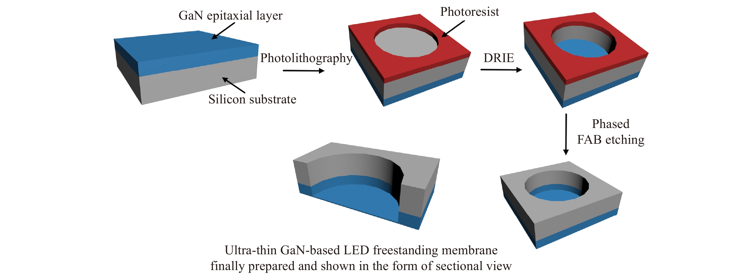
The backside process for preparing the ultra-thin GaN-based LED freestanding membrane is shown in Fig. 1. At first, a round structure with different diameters is fabricated on the silicon substrate surface behind the wafer through photolithography. Then the silicon substrate in the round structure is hollowed out by DRIE to form the GaN-based LED freestanding membranes with different diameters. Finally, an ultra-thin GaN-based LED freestanding membrane device of sub-micron thickness is prepared by using the highly controllable FAB etching technology to reduce the backside thickness of LED freestanding membrane by stages. Among the technologies, FAB etching technology is the key to the preparation process. This technology uses the electron beam generated by directional high-voltage current (1.8 kV, 12 mA) to accelerate the SF6 atoms, and performs the high-precision anisotropic etching of GaN material at a stable speed. The etching depth precision of GaN material can be up to the nanometer level.
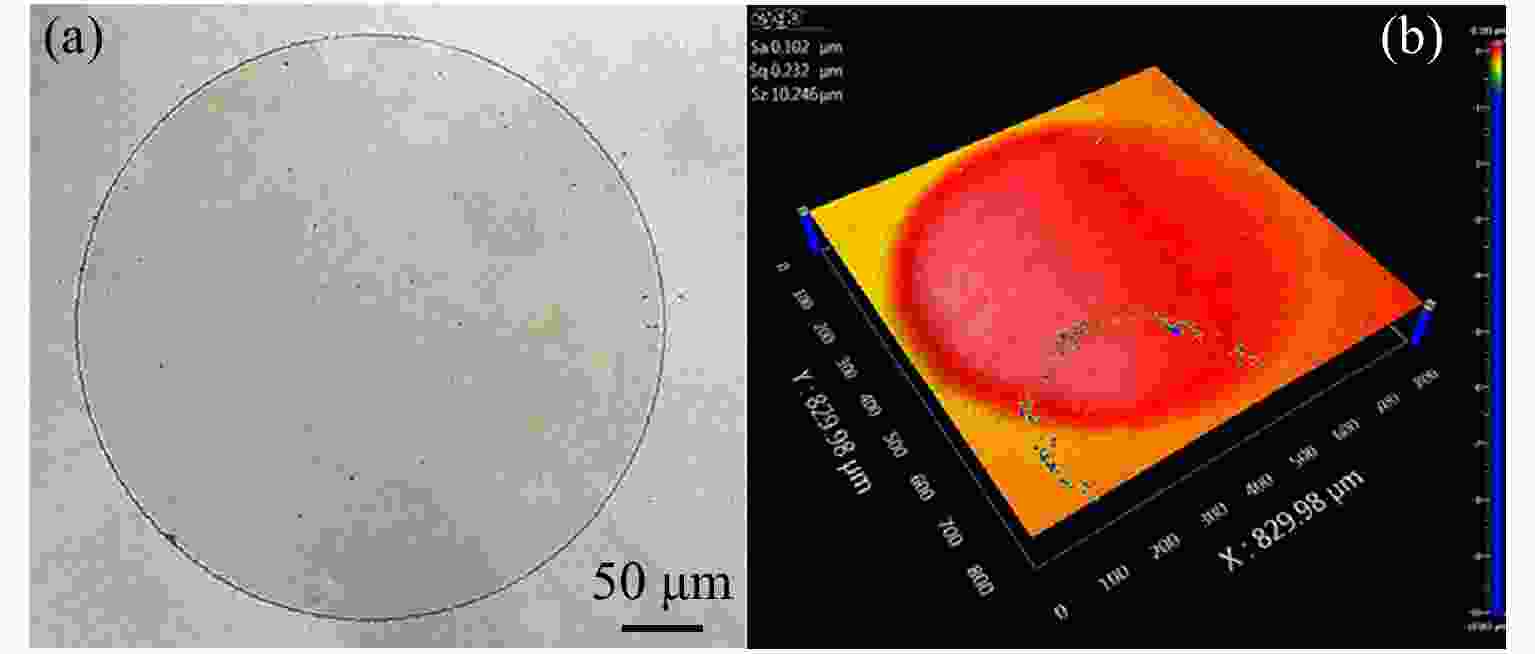
In order to study the deformation and stress release rules of the LED freestanding membranes in different sizes, we designed four types of round LED freestanding membranes with different diameters (100, 200, 400 and 800 μm). The membrane areas range from 31 400 μm2 to 2 009 600 μm2, covering the possible sizes of GaN-based MOMES system. The Fig. 2 (color online) shows the LED freestanding membrane with a diameter of 800 μm observed by optical morphological detector. The Fig. 2(a) shows the 2D morphological characteristics of the LED freestanding membrane observed from the front by optical microscope, while the Fig. 2(b) shows the 3D deformation of the membrane tested by white light interferometer. It can be seen from Fig. 2 that the LED freestanding membrane with a diameter of 800 μm still has good surface quality without cracks or other defects after the silicon substrate is hollowed out, which proves the feasibility of backside process. Due to the presence of stress between GaN epitaxial layer and silicon substrate, the membrane as a whole presents smooth arch deformation after the release of internal stress.
The LED freestanding membranes with different diameters and thicknesses prepared by backside process have different surface deformations, as can be seen in Fig. 3 (color online). The surface deformation increases with the membrane diameter and decreases with the membrane thickness. The membrane as a whole presents the arch deformation with a bulging center and a smooth edge. For the LED freestanding membrane with the silicon substrate peeled only (about 4.9 μm thick), its maximum deformation is about 400 nm when its diameter is 800 μm, and about 100 nm when its diameter is 100 μm. For the LED freestanding membrane thinned once on the backside to about 2 μm, its maximum deformation is about 300 nm when its diameter is 800 μm, and about 100 nm when its diameter is 100 μm. For the membrane thinned twice on the backside to about 600 nm (submicron thickness), its maximum deformation is about 100 nm when its diameter is 800 μm, and about 40 nm when its diameter is 100 μm. When the membrane is thinned on the backside to submicron thickness, its overall deformation is significantly reduced.
3. Optical characterization of ultrathin GaN-based LED freestanding membrane
In the above text, we studied and analyzed the morphological characteristics of ultrathin GaN-based LED freestanding membrane. In this section, we will study its optical characteristics and analyze how to improve its optical performance. We will also use a reflectance spectrometer to test the membranes that have been thinned on the backside to different thicknesses. With the wavelength range of 450~850 nm, the reflectance spectrometer tests the reflectance spectrum of the membranes from the normal incident direction. The reflected light on the membrane surface and that on the bottom interface interferes with each other. The resulting reflectance spectrum can be used to characterize the membrane thickness and the number of modes. The thicker the membrane, the more the harmonic peaks (the number of modes) caused by interference.
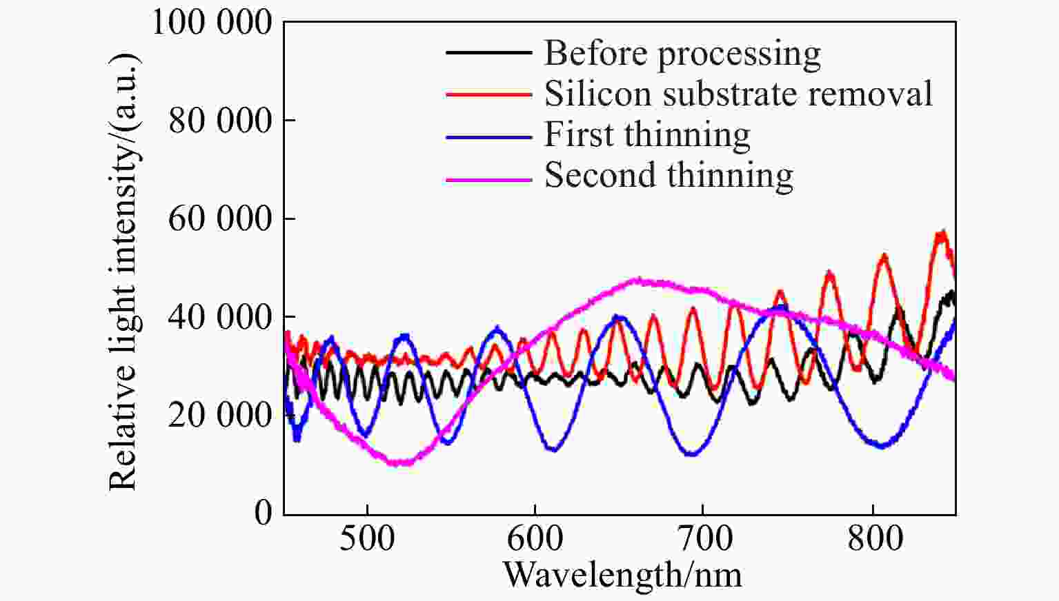
For the silicon-based GaN sample without backside processing, the total thickness of its GaN epitaxial layer, including silicon substrate, is 4.9 μm. In the Fig. 4 (color online), the number of its reflection modes is 27, and the overall relative light intensity of its reflectance spectrum is low. For the LED freestanding membrane with silicon substrate removed, its thickness remains unchanged, and the number of its reflection modes is still 27. However, due to the removal of silicon substrate, the reflected light absorbed by the sample is reduced, and the relative light intensity of reflectance spectrum is increased. For the LED freestanding membrane thinned once on the backside to about 2 μm, the number of its reflection modes is reduced to 6. For the membrane thinned twice on the backside to about 600 nm, the number of its reflection modes is finally reduced to 1. A smaller membrane thickness contributes to the application of LED freestanding membrane to the MOMES devices requiring precise operation and control. Fewer interference modes of the membrane can help deliver more easily the outgoing light generated by the active layer of LED device, and improve the luminous efficiency of the device.
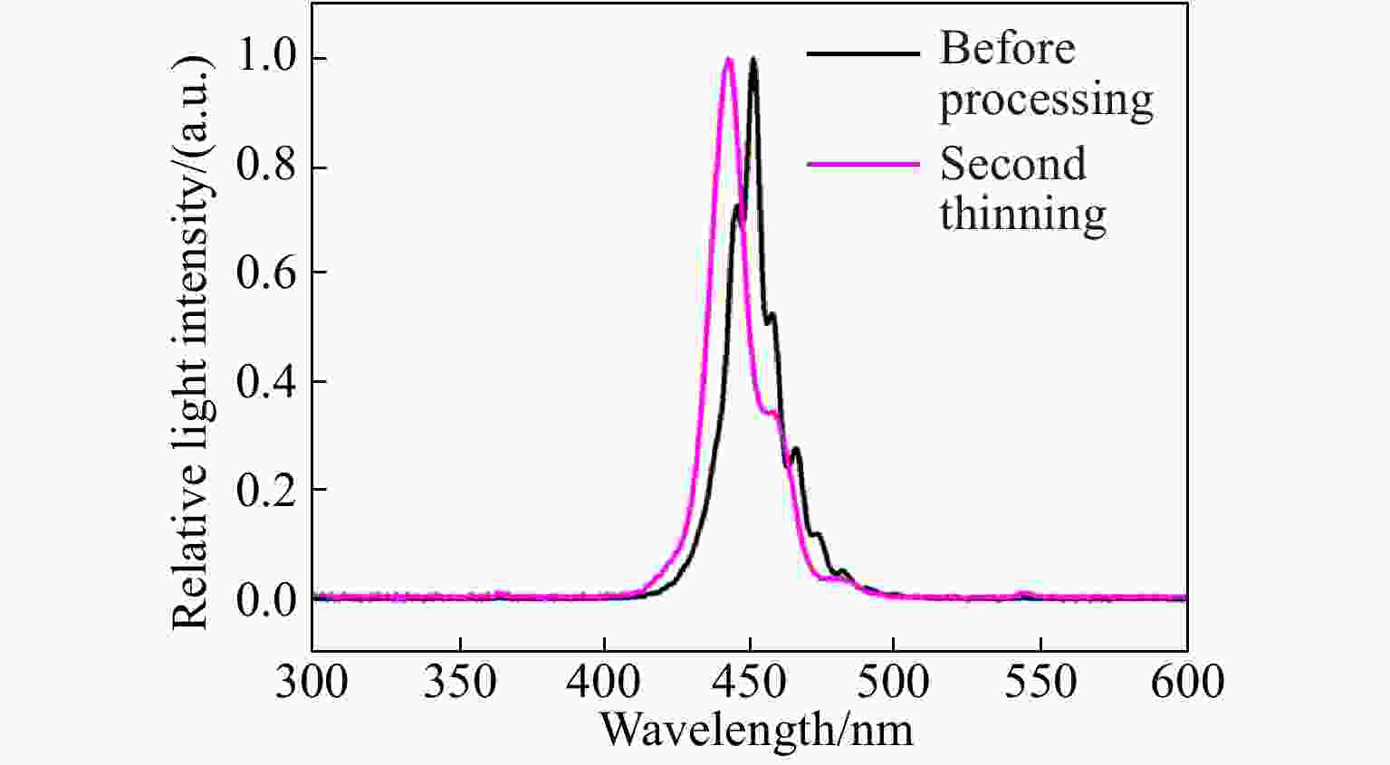
After that, a He-Ne laser with a wavelength of 325 nm is used to excite the active layer of quantum well of LED freestanding membrane to generate the emergent light, which is then tested for photoluminescence and for spectrum measurement by a wide-spectrum spectrometer. Due to the large lattice mismatch and thermal mismatch between silicon substrate and GaN epitaxial layer, a thick Al(Ga)N buffer layer is introduced into the GaN epitaxial layer to compensate for the lattice mismatch and thermal expansion. There is a large internal stress between silicon substrate and GaN epitaxial layer. Under the condition of photoluminescence excitation from the membrane front, we have studied the photoluminescence spectrum where the internal stress between GaN epitaxial layer and silicon substrate is released through the backside process. After the release of internal stress, the quantum well band structure of LED freestanding membrane will change, resulting in the corresponding change of its photoluminescence spectrum. As can be seen from Fig 5 (color online), the peak wavelength of the light emitted from the membrane is 450.7 nm before the backside processing, and is 442.5 nm after being thinned twice. Since the interface between silicon substrate and GaN epitaxial layer and the thick Al(Ga)N buffer layer are removed by backside process, the released internal stress causes the change of the quantum well band structure so that the peak wavelength of the outgoing light in photoluminescence shows a significant blue shift of 8.2 nm.
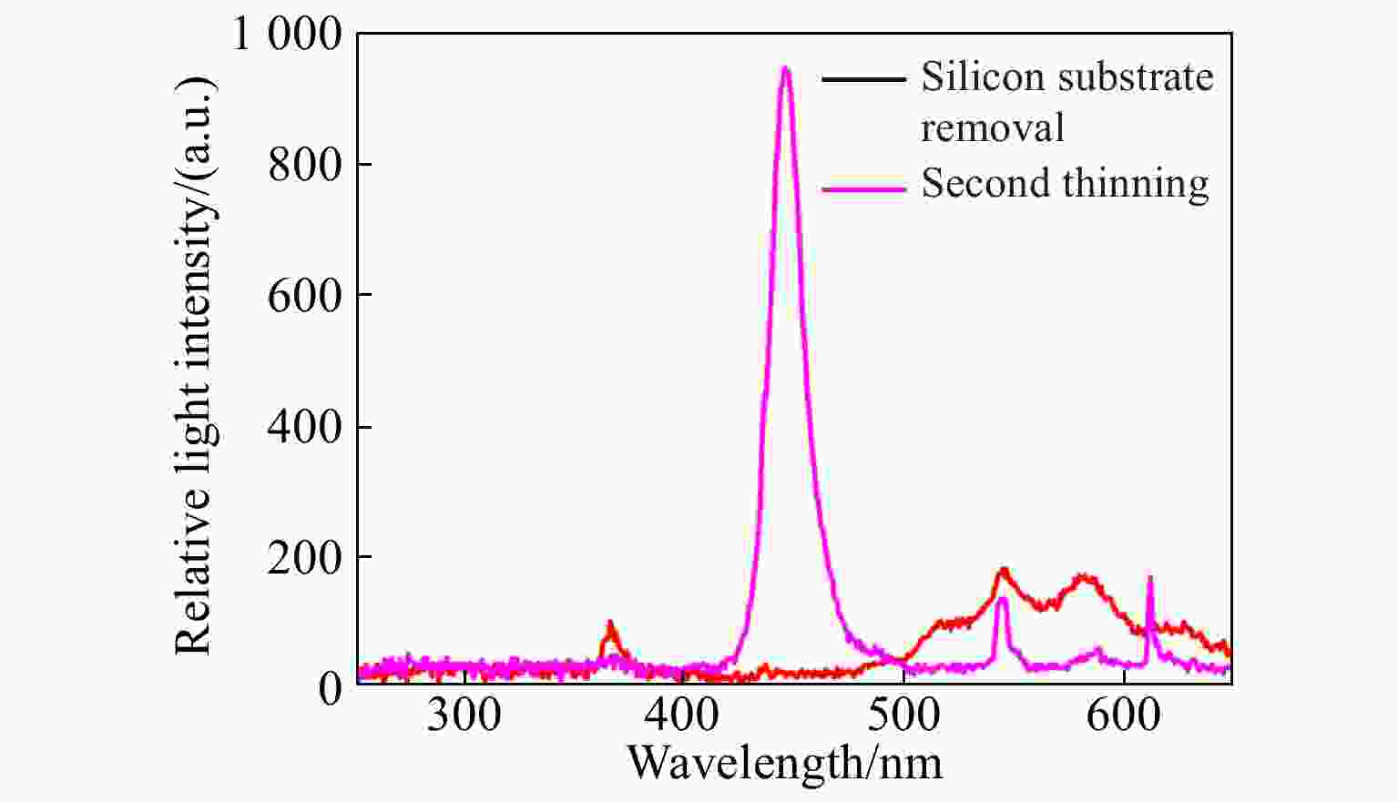
As shown in Fig. 6 (color online), in the photoluminescence test on the backside of a LED freestanding membrane, no light obviously exits from the membrane with only silicon substrate removed, and most of the light out of the backside is absorbed by GaN epitaxial layer. In addition, since the thicker membrane has more interference modes, the export of emergent light is also affected. After the backside is thinned twice, most of the epitaxial layer is removed and the thickness of the membrane is reduced to about 600 nm. As most of the epitaxial layer that absorbs the light out of the backside has been removed and the interference modes of the membrane have been decreased, the light out of the membrane backside can be obviously detected.
4. Conclusion
In this paper, an ultra-thin GaN-based LED freestanding membrane based on the backside process has been obtained by using a silicon-based gallium nitride wafer. By peeling off the silicon substrate through deep reaction ion etching and thinning the backside of GaN epitaxial layer through FAB etching, the epitaxial layer was thinned from 4.9 μm to about 600 nm. We studied the deformation and optical characteristics of LED freestanding membranes with different thicknesses and sizes. The overall membrane deformation increases with the membrane diameter and decreases with the membrane thickness. The membrane as a whole presents the arch deformation with a bulging center and a smooth edge. After the backside thinning, the deformation of the membrane with a diameter of 800 μm decreases from 400 nm to 100 nm. The reflectance spectrum test shows that the freestanding membrane with a thickness of 4.9 μm has 27 interference modes, while the membrane with a thickness of 600 nm has only 1 interference mode. The front photoluminescence test shows that the release of internal stress generated by the backside process causes the change of quantum well band structure. Compared with unprocessed silicon-based gallium nitride wafer, the spectral peak of the 600 nm thick membrane has a blue shift of 8.2 nm. In the photoluminescence test on the backside, obvious outgoing light can also be detected from the ultra-thin LED freestanding membrane with most of the GaN epitaxial layer removed. With small overall deformation, a large round LED freestanding membrane of submicron thickness can be applied to the MOMES system requiring precise operation and control. Fewer interference modes of the membrane can help derive more easily the outgoing light generated by the active layer of LED device. This membrane provides a new way for the application of GaN-based LED device in the field of MOMES.
-
-
[1] PEARTON S J, ZOLPER J C, SHUL R J, et al. GaN: processing, defects, and devices[J]. Journal of Applied Physics, 1999, 86(1): 1-78. [2] ZHANG Y H, DADGAR A, PALACIOS T. Gallium nitride vertical power devices on foreign substrates: a review and outlook[J]. Journal of Physics D:Applied Physics, 2018, 51(27): 273001. doi: 10.1088/1361-6463/aac8aa [3] NAKAMURA S, PEATRON S, FASOL G. The Blue Laser Diode: the Complete Story[M]. 2nd ed. Berlin: Springer, 2000. [4] ALHASSAN A I, YOUNG E C, ALYAMANI A Y, et al. Reduced-droop green III-nitride light-emitting diodes utilizing GaN tunnel junction[J]. Applied Physics Express, 2018, 11(4): 042101. doi: 10.7567/APEX.11.042101 [5] LI B, REN Y, CHANG B K. Stability of gradient-doping GaN photocathode[J]. Chinese Optics, 2018, 11(4): 677-683. (in Chinese) doi: 10.3788/co.20181104.0677 [6] MORELLE C, THÉRON D, DERLUYN J, et al. Gallium nitride MEMS resonators: how residual stress impacts design and performances[J]. Microsystem Technologies, 2018, 24(1): 371-377. doi: 10.1007/s00542-017-3293-0 [7] YANG ZH CH, LÜ J N, YAN G ZH, et al. Fabrication of GaN-based MEMS structures using dry-etch technique[J]. Nanotechnology and Precision Engineering, 2011, 9(1): 78-82. doi: 10.3969/j.issn.1672-6030.2011.01.015 [8] LI X, SHI ZH, HE SH M, et al. MEMS-tunable Ⅲ-nitride grating on silicon substrate[J]. Optics and Precision Engineering, 2014, 22(11): 2945-2949. (in Chinese) doi: 10.3788/OPE.20142211.2945 [9] TABATABA-VAKILI F, ROLAND I, TRAN T M, et al. Q factor limitation at short wavelength (around 300 nm) in III-nitride-on-silicon photonic crystal cavities[J]. Applied Physics Letters, 2017, 111(13): 131103. doi: 10.1063/1.4997124 [10] PRABASWARA A, MIN J W, ZHAO CH, et al. Direct growth of III-nitride nanowire-based yellow light-emitting diode on amorphous quartz using thin Ti interlayer[J]. Nanoscale Research Letters, 2018, 13(1): 41. doi: 10.1186/s11671-018-2453-1 [11] LI T P, ZHAO G ZH, LU T P, et al. Effect of Undoped GaN layer thickness on the wavelength uniformity of GaN based blue LEDs[J]. Chinese Journal of Luminescence, 2017, 38(9): 1198-1204. (in Chinese) doi: 10.3788/fgxb20173809.1198 [12] ZHOU ZH Y, YANG K, HUANG Y M, et al. Recombination Process in InGaN/GaN MQW LED on Silicon with δ-Si Doped n-GaN Layer[J]. Chinese Journal of Luminescence, 2018, 39(12): 1722-1729. (in Chinese) doi: 10.3788/fgxb20183912.1722 [13] CHARLES M, MRAD M, KANYANDEKWE J, et al. Extraction of stress and dislocation density using in-situ curvature measurements for AlGaN and GaN on silicon growth[J]. Journal of Crystal Growth, 2019, 517: 64-67. doi: 10.1016/j.jcrysgro.2019.04.014 [14] WANG K J, WANG A Q, JI Q B, et al. Epitaxy of GaN in high aspect ratio nanoscale holes over silicon substrate[J]. Applied Physics Letters, 2017, 111(25): 252101. doi: 10.1063/1.5002529 [15] ISHIKAWA H, ASANO K, ZHANG B, et al. Improved characteristics of GaN-based light-emitting diodes by distributed Bragg reflector grown on Si[J]. Physica Status Solidi (A) , 2004, 201(12): 2653-2657. [16] ISHIKAWA H, JIMBO T, EGAWA T. GaInN light emitting diodes with AlInN/GaN distributed Bragg reflector on Si[J]. Physica Status Solidi C, 2008, 5(6): 2086-2088. doi: 10.1002/pssc.200778441 [17] ZHANG B J, EGAWA T, ISHIKAWA H, et al. Thin-film InGaN multiple-quantum-well light-emitting diodes transferred from Si (111) substrate onto copper carrier by selective lift-off[J]. Applied Physics Letters, 2005, 86(7): 071113. doi: 10.1063/1.1863412 [18] CHEN T F, WANG Y Q, XIANG P, et al. Crack-free InGaN multiple quantum wells light-emitting diodes structures transferred from Si (111) substrate onto electroplating copper submount with embedded electrodes[J]. Applied Physics Letters, 2012, 100(24): 241112. doi: 10.1063/1.4729414 [19] LUO R H, RAO W T, CHEN T F, et al. Vertical InGaN multiple quantum wells light-emitting diodes structures transferred from Si (111) substrate onto electroplating copper submount with through-holes[J]. Japanese Journal of Applied Physics, 2012, 51(1R): 012101. doi: 10.7567/JJAP.51.012101 [20] HUANG B B, XIONG CH B, TANG Y W, et al. Changes of stress and luminescence properties in GaN-based LED films before and after transferring the films to a flexible layer on a submount from the silicon epitaxial substrate[J]. Acta Physica Sinica, 2015, 64(17): 177804. (in Chinese) doi: 10.7498/aps.64.177804 期刊类型引用(5)
1. 刘翠翠,林楠,马骁宇,张月明,刘素平. 多变量Si杂质诱导InGaAs/AlGaAs量子阱混杂研究. 中国光学(中英文). 2023(06): 1512-1523 . 百度学术
2. 蒋成伟,沙源清,袁佳磊,王永进,李欣. 电致发光的完全悬空超薄硅衬底氮化镓基蓝光LED器件的制备与表征. 中国光学. 2021(01): 153-162 . 百度学术
3. 傅康,王永进,绪锌羽. 基于LED同质集成效应的智慧屏幕系统. 南京邮电大学学报(自然科学版). 2021(01): 51-57 . 百度学术
4. 王世龙,熊传兵,汤英文,李晓珍,刘倩. 共晶芯片数及芯片位置对陶瓷共晶封装LED发光性能的影响. 发光学报. 2020(11): 1421-1430 . 百度学术
5. 王永进,傅康,王林宁. 一种基于可见光通信技术的光互联方案. 南京邮电大学学报(自然科学版). 2020(05): 134-140 . 百度学术
其他类型引用(1)
-