留言板

尊敬的读者、作者、审稿人, 关于本刊的投稿、审稿、编辑和出版的任何问题, 您可以本页添加留言。我们将尽快给您答复。谢谢您的支持!

姓名
邮箱
手机号码
标题
留言内容
验证码

非对称轻小型头盔显示器光学系统设计

黄颂超 冯云鹏 程灏波

常改艳, 王玉恒, 程光华. 超快贝塞尔光束在硫化锌晶体表面制备纳米孔[J]. 中国光学(中英文), 2021, 14(1): 213-225. doi: 10.37188/CO.2020-0101
引用本文: 黄颂超, 冯云鹏, 程灏波. 非对称轻小型头盔显示器光学系统设计[J]. 中国光学(中英文), 2020, 13(4): 832-841. doi: 10.37188/CO.2019-0193
CHANG Gai-yan, WANG Yu-heng, CHENG Guang-hua. Writing nanopores on a ZnS crystal with ultrafast Bessel beams[J]. Chinese Optics, 2021, 14(1): 213-225. doi: 10.37188/CO.2020-0101
Citation: HUANG Song-chao, FENG Yun-peng, CHENG Hao-bo. Non-symmetrical design of a compact, lightweight HMD optical system[J]. Chinese Optics, 2020, 13(4): 832-841. doi: 10.37188/CO.2019-0193

非对称轻小型头盔显示器光学系统设计

基金项目: 深圳市科技创新项目(No. JCYJ20170817115037194,No. JCYJ20180307123816647)
详细信息
    作者简介:

    黄颂超(1994—),男,福建泉州人,硕士,助理工程师,主要从事成像光学设计方面的研究。E-mail:478886527@qq.com

    冯云鹏(1981—),男,河北邯郸人,博士,讲师,2011年于北京理工大学获得博士学位,主要从事新型光学系统先进光学制造与检测方面的研究。E-mail:roc@bit.edu.cn

  • 中图分类号: TN141;O439

Non-symmetrical design of a compact, lightweight HMD optical system

Funds: Shenzhen Science and Technology Innovation Project (No. JCYJ20170817115037194, No. JCYJ20180307123816647)
More Information
  • 摘要: 针对非对称光学系统视场范围和出瞳直径较窄、光学结构复杂、制造成本昂贵、装配调整麻烦等问题,本文采用在系统中加入自由曲面反射镜的设计方法。首先,论述了双反射镜非对称光学系统的设计要求和工作原理。然后,分析了三反射镜非对称光学系统的离轴结构控制方法。最后,采用XY多项式自由曲面反射镜折叠光路、消除遮拦、扩大视场、校正离轴像差,设计出一款适用于头盔显示器的非对称光学系统。设计的双反射镜非对称光学系统的视场为60°×30°,出瞳直径为8 mm。在截止频率52 lp/mm处,全视场的调制传递函数值大于0.25,系统畸变小于5%,单目系统重量约为190 g。设计结果表明,该非对称光学系统的视场大小和成像质量均有所提升,实现了小型轻量化,可应用于头盔显示器。


  • The mid-infrared photonics has attracted considerable attention because its wavebands cover thermal imaging bands, multiple atmospheric windows (3~5 μm and 8~14 μm) necessary for free space communication, as well as main absorption bands of most chemical and biological molecules. It is an inevitable trend for photonic integration to cut costs, improve performance and miniaturize special optical instruments, for example, micro-scale photonic circuits are manufactured in optical materials with a transparent window up to 20 μm. The application of integrated photonics has promoted the rapid development of optical communication technology and the expansion of applied wavelength from near infrared to middle and far infrared. However, the infrared window materials in medium and long wave bands are very limited, mainly including GaAs, GaP, ZnSe, ZnS, InSb, etc.[1-4]. Considering the optical and mechanical properties of these materials, ZnS crystal has become one of the most promising infrared optical materials due to its advantages such as low absorption, high hardness, large Young's modulus, wide transparent window (0.37~14 µm) and good chemical stability[5]. The performance of photonic devices is related to nonlinear optics, the response of materials to the interaction between light and matter, and the balance between the relaxation processes of materials. This means that it is necessary to precisely control the interaction between light and matter and the size of photonic devices so as to realize effective optical transmission and control in complex optical systems.

    Ultra-fast Bessel pulse laser is the combination of ultra-fast laser pulse and spatial beam shaping (zero-order Bessel beam) and is formed by symmetric interference between the plane wave and the wave vector distributed on the conic bus. It has a long non-diffraction transmission distance (focal depth DOF = W/2·tanθ, where W is the radius of incident Gaussian beam and θ is the beam half-cone angle in the Bessel region) and good transmission robustness (self-recovery)[6-8]. An ideal Bessel beam has a narrow and strong central interference region[9-10]. This indicates that the Bessel beam is superior to the Gaussian beam in the micro-nano machining of extended micro-channels. For example, the Bessel beam has been used to successfully prepare the nanopore micro-channel structure with a aspect ratio of 10000:1 in borosilicate glass[11-13]. In addition, ultra-fast Bessel laser pulses have shown strong applicability in the high-depth and large-area machining, the micro-nano welding, and the development of a mix of micro-nano scale features with new photonic functions[6,12-14]. Although ZnS crystal is one of the most promising infrared window materials, its high nonlinear coefficient can cause serious distortion of temporal and spatial distribution of laser pulses when the focused femtosecond laser is transmitted in this crystal. Moreover, the self-focusing and the self-defocusing of plasma can cause spatial beam splitting so that the laser energy cannot be effectively concentrated on the focus. Early experimental and theoretical studies showed that the peak power density could be effectively reduced by pulse broadening, thus weakening the nonlinear effect. 15ps-20ps Ti-sapphire pulsed laser can effectively absorb laser energy and write waveguide in sulfide glass. In the early stage, ultra-fast Bessel beam was used to fabricate the nanopores mainly in quartz glass, silicate glass and borosilicate glass, whose nonlinear absorption was different from that of ZnS by orders of magnitude. Secondly, the hardness, thermal diffusion coefficient and Young's modulus of ZnS crystal are also significantly different from those of the above glass. Therefore, it is difficult to fabricate nanopores on ZnS crystal with ultrafast laser. So far, the preparation of periodic subwavelength microstructures on ZnS crystal has been reported[15]. However, the use of ultrafast laser to process the nanopores with high aspect ratio on ZnS crystal is still in blank. In Ref. [16], we reported and discussed the influence of beam mode on the quality of drilling on ZnS crystal. The experimental results show that on ZnS crystal, the pore-forming quality of Bessel beam is better than that of Gaussian beam. Therefore, the use of Bessel laser to directly write nanoscale microstructures on ZnS crystal, to prepare various medium-infrared optical components and to improve or achieve one of their capabilities has become the current research hotspot of medium-infrared integrated photonics, with a broad application prospect.

    In this paper, a Yb:KGW femtosecond laser with the central wavelength of 1030 nm, the repetition frequency of 100 kHz, and the pulse width of 223 fs was used to generate the Gauss-Bessel beam through an axicon. Then the parameter ranges of the nanopores fabricated on the surface of ZnS crystal were studied. The morphology of nanopores was analyzed by using a Focusing Ion Beam (FIB, Helios G4 CX) and a Scanning Electron Microscope (SEM, JEOL JSM-7500F). The dependence of the surface morphology, diameter and depth of nanopores on laser pulse energy and pulse width was determined. The potential applications of nanopores were discussed.

    The Bessel beam generation device described in Ref. [8], as shown in Fig. 1, is used in this experiment. Firstly, the beam is expanded to 8 mm, and the beam diameter will affect the focusing depth. Applying a combination of an axicon with 1° base angle (Altechna, 1-APX-2-H254-P, n = 1.45), focusing lens L1 with focal length f1 = 400 mm, and the 20× near-infrared focusing objective lens L2 with f2 = 10 mm (Mitutoy NIR, numerical aperture NA = 0.42, working distance L= 20 mm), and using a spatial filtering system, we build an experimental device for generating zero-order Bessel beam laser direct-writing microstructure. A Yb:KGW mode-locked regenerative laser amplification system (Pharos, Light Conversion) with a central wavelength of 1030 nm and adjustable repetition frequency is used to write nano-pore microstructures on ZnS crystal. The pulse width can be continuously adjusted within 223 fs~25 ps by a removable grating compressor in the laser system. The energy of laser pulse is regulated by a half-wave-plate Polarized Beam Splitter (PBS). The sample where the nanopores are written is an 18 mm×8 mm×2 mm four-sided polished ZnS crystal. It is fixed to a computer-controlled XYZ 3D high-precision air bearing platform (Aerotech, ANT130). A focusing lens is used to focus the beam on the sample. A high-precision (75 nm) NC system is used to move the sample at a constant speed during the irradiation with a continuous laser pulse. The nanopore spacing can be adjusted by the repetition frequency of the laser source and the translational velocity of the sample (Λ = v/f). During continuous laser irradiation, the Aerotech platform moves the sample at a constant speed (in the positive direction of X-axis) and simultaneously moves the relative movement with respect to the laser focus (in the negative direction of Z-axis) to ensure that a new exposure area is always placed in the laser action area. This writing method can help observe the dynamic evolution process of the pore diameter inside the polished sample.

    Figure  1.  Experimental setup for microchannel writing with Bessel laser

    The focusing ultrashorter laser pulse has ultra-high peak power and can selectively induce a series of nonlinear effects of transparent materials, such as multi-photon absorption, Kerr effect, plasma self-focusing and self-defocusing, so as to change the microregion morphology and molecular structure of the materials[17]. For the ultra-fast laser with a pulse width of 20 ps and a wavelength of 1 μm, its air ionization threshold is approximately 2.7×10¹³ W/cm2[18]. It can be calculated that, in this experiment, the laser power density range acting on ZnS crystal is 0.57×10¹³~6.02 ×10¹³ W/cm2. When the laser power density is greater than the ionization threshold of air or ZnS crystal, the laser pulse will generate strong nonlinear absorption in the focus area and cause the formation of plasma, thus effectively absorbing the laser energy and forming a local deposition area with high energy density[19]. The extreme high temperature and pressure in the focus area leads to phase transition and micro-explosion, and the energy diffuses from the focus area to the surrounding material in the form of shock wave, so as to construct a 3D micro-nano structure inside the transparent material[20-22]. By discussing and analyzing the deposition energy from the nonlinear transmission of laser pulse inside transparent material as well as the possible thermal mechanism, the phase change and the formed microstructural morphology can be controlled more easily. For the laser parameters and air/ZnS crystal interface issue in this experiment, the nonlinear Schrodinger equation in common use can be used to calculate the concentration of plasma in the focus region. However, the mechanism of micro-explosion on the air/crystal interface is more complex. By referring to the parameters and law of femtosecond laser waveguide writing on quartz glass and sulfide glass[23-24], this experiment studied the features of the microstructure fabricated by Bessel beam on ZnS crystal surface when the pulse width changed from femtosecond to 20 ps and the energy changed from damage threshold to 63 μJ. The FIB, SEM and phase contrast microscope (PCM, Olympus BX51) were used to characterize the morphology and length of nanopores and micro-channels on the sample surface and determine the dependence of surface morphology, diameter and depth of nanopores on laser pulse energy and pulse width.

    Pulse energy and pulse width are the key parameters that affect the interaction between laser and matter. Pulse energy determines the effective radiation flux that the unit area of material is exposed to in unit time. Pulse width is related to the axial energy deposition efficiency of Bessel laser beam[6,25]. The experimental and numerical results of the interaction between ultrafast beam and quartz glass and of micro-nano fabrication show that several picoseconds of pulses can effectively overcome the decrease of laser focus plasma density caused by strong nonlinear effects. Considering spatial and temporal focusing characteristics, the nonlinear numerical simulation results of this material show that the plasma concentration generated by the 4.7-ps pulse ionized at the focal point is one order of magnitude higher than that generated by the 60-fs pulse of the same energy[6]. However, the nonlinear absorption coefficient of ZnS is one order of magnitude higher than that of common glass, so in the process of pulse width optimization, the range of pulse variation needs to be increased. During the experiment, the maximum pulse width was adjusted to 25 ps by adjusting the compressor of the regenerative amplifier to cover the writing range of the sulfide waveguide[26]. When the laser pulse width was increased from 10 ps to 20 ps, the damage threshold range of the ZnS crystal used in this experiment was 6.51~8.32 J/cm2. The detailed measurement and calculation methods have been reported in Ref. [27].

    The Fig. 2 is a picture of the nanopores on the sample surface, which was obtained from SEM characterization without any post-treatment. During the SEM morphology characterization, the ZnS surface was coated with a gold film about 50 nm thick to become conductive. The black dots at the center of the white ring are nanopores, each of which is written with a single pulse. The white halo around the nanopores is formed by the sputtering or redeposition of the material removed during laser processing. Similar material deposition principles have been reported in Ref. [28]. ZnS crystal is an important wideband infrared window material with strong photosensitivity and inherent sub-stability. Its band gap width is 3.6~3.8 eV. Under the 1030-nm infrared laser radiation, it performs the three-photon absorption. Its nonlinear absorption coefficient (a3 = 0.5×10⁻³ cm3/GW2) is two orders of magnitude higher than quartz glass. These characteristics indicate the necessity of spatiotemporal envelope control of ultrafast laser pulses[15]. Pulse width is a parameter sensitive to ZnS crystal surface damage. The Fig. 2 shows that 12.5-ps pulse width is the critical value where a nanopore will occur. When the pulse width was less than 12.5 ps, the nanopores with a aspect ratio did not appear in the pulse energy range of 35.83~62.82 μJ. Instead, the pits with certain depth appeared, as shown in the left column of Fig.2. This is because under short-duration pulses, the carrier generation speed is faster and the plasma defocusing efficiency is higher, so that the axial energy deposition density will be reduced and the thermodynamic conditions for micro-explosion can't be met[29].

    The Fig. 3 shows the dependence of nanopore diameter on the pulse width and energy of Bessel beam. The minimum nanopore diameter on ZnS crystal surface was measured by SEM to be 80 nm, and was written by the laser with a pulse width of 12.5 ps and pulse energy of 48.67 μJ. The curves in Fig. 3 show that when the pulse energy is fixed, the nanopore diameter will increase with the pulse width within the pulse width window of 12.5~20 ps. When the pulse width is fixed, the nanopore diameter will increase with the pulse energy. Moreover, the greater the energy is, the more obvious this trend will be. However, this does not seem to be the case at the pulse width of 12.5 ps. Since pulse width is a parameter sensitive to crystal surface ablation, the laser near the critical pulse width 12.5 ps can cause various nonlinear effects to interact with each other and result in the instability of nanopore. All the experiments in this paper demonstrate the damage characteristics under monopulse action, which are significantly different from the results of multi-pulse action[30]. As far as monopulse is concerned, the self-organizing interference is difficult to occur, and the modulation of laser intensity in the focus area and of plasma intensity is not obvious.

    Figure  2.  SEM images of nanopores on ZnS surface at various pulse energies. (a) 35.83 μJ; (b) 48.67 μJ; (c) 62.82 μJ. The laser pulse widths in columns 1 to 4 are 10 ps, 12.5 ps, 15 ps and 20 ps respectively
    Figure  3.  Nanopore diameter on ZnS crystal surface changes with pulse energy under different laser pulse widths

    The dynamic process of nanopore formation is generally divided into three stages. The first stage is the nonlinear absorption of crystal and the distortion of pulse space-time. In this stage, different laser parameters directly affect the absorption and deposition of energy in the focus area. The second stage is plasma relaxation, which includes the release of backscattering pressure of high temperature electrons and the transfer of electron energy to the lattice to cause lattice heating and deformation. The third stage is mainly thermal process and lattice relaxation lasting from picoseconds to microseconds. The change of refractive index of quartz glass under the action of ultra-fast Bessel beam can be seen from time-resolved phase contrast photographs and plasma luminescence intensity. For example, the refractive index of fs time window decreases, that of ps window increases, and those of ns and μs time windows decrease. However, it is difficult to determine whether the nanopores are formed in the femtosecond stage or nanosecond stage. Both the backscattering pressure of the electrons and the rapid expansion caused by thermal effect may lead to micro-explosion. The self-focusing and self-defocusing effects in nonlinear absorption process and the Rayleigh Taylor instability in fluid dynamics process will lead to the irregular change of nanopore diameter[19].

    AFM, SEM and other surface analysis tools are powerless to characterize the 3D morphology of the nanopores with high depth-diameter ratio. Therefore, in order to obtain the longitudinal morphology features of nanopores, the characterization method of "FIB denudation +SEM imaging" was selected. The FIB etching process enables us to minimize the damage to one-dimensional Bessel pores so that we can analyze the longitudinal morphology of nanopores more intuitively. The results of SEM surface characterization showed that, under 20-ps pulse width and 62.82-μJ pulse energy, the nanopore structure on the surface of ZnS crystal was an oval rather than a regular circle occurring under other laser parameters. Under overhigh peak power density, the Bessel beam was subjected to unexpected nonlinear effects on the crystal surface, which affected the normal transmission of the beam. The possible influencing mechanisms include: Kerr self-focusing, plasma self-defocusing, multi-photon ionization, and plasma shielding. These effects work together to constrain the strength of the Bessel beam on the material surface. Therefore, 20-ps pulse width and 48.67-μJ pulse energy are selected as the laser parameters for follow-up study.

    The Fig.4 shows the nanopore structure prepared under 20-ps pulse width and 48.67-μJ pulse energy. It can be seen that, the pore channel has a variable diameter along the laser transmission direction. This has something to do with the distribution of axially deposited energy density of Bessel pulse laser during the nonlinear optical transmission inside the material.[6]. The appearance of pore wall indicates that the material has undergone a process of melting and resolidification. The white flake on the microstructure surface is the residual of the gold film which was applied on the sample surface for conductive use during the SEM characterization and then ultrasonically cleaned. The chemical composition of the white flake was characterized by energy spectrometer (EDS). The results showed that the flake was gold. The lamination diagram along the FIB etching direction is helpful to observe the morphological changes of pore microchannels during the etching process. It can be seen that the pore microchannel transitions from about 3 μm to a larger length as the FIB etching goes on. Because the FIB etching direction can't be easily aligned to the extension direction of the pore, the information on nanopores isn't exhaustive in this paper. To learn more about the pore depth, we observed the side of the nanopore by optical phase contrast microscope.

    Figure  4.  SEM image of cross section of FIB-etched nanopore

    The Fig. 5(b) shows the side view of pore microchannels under a 20× phase contrast microscope (transmission type). In the PCM transmission-type microscope, the phase shift corresponding to negative refractive index change looks darker on the gray background. For quartz glass, the black traces indicate that the increase in refractive index, while the white traces is the nanopore or gratings with decreasing refractive index. But for sulfide glass with high refractive index, the change of refractive index cannot be judged by diffraction contrast. On the one hand, the refractive index varies greatly and the phase may be inverted; on the other hand, the indication left after laser damage has strong scattering[25]. The above enlarged view shows that the micro-channels have good uniformity without fault. The nanopore fabricated on ZnS crystal by 20 ps/48.67 μJ Bessel laser pulse is about 270 μm long. The refractive index of ZnS crystal is higher than that of quartz glass. If there is no nonlinear effect, the effective length of Bessel beam focus in the ZnS crystal should be larger than that of quartz glass. However, both the simulation and experimental results show that the length of nanopore in ZnS is only half of that in quartz glass. The main reason is that the travel of a nanopore is a highly nonlinear process. It is difficult to derive the law of pore pattern change in the two materials from a single parameter. To explore the positive morphology and pore size change of nanopores inside the material, the sample surface was repeatedly polished, gold-plated and characterized by SEM. The Fig. 5(a) is a SEM image of the cross section of the polished micro-channel. The measurement results show that the pore diameter is about 180 nm, 40 nm smaller than the unpolished diameter. To verify the operability and repeatability of microchannels, several pore microchannels spaced 15 μm apart were processed on the ZnS crystal by using the Bessel beams with the same pulse width and energy (20 ps, 48.67 μJ). Three of them are shown in 5(b). From Fig. 4 and Fig. 5, the accurate information on nanopore depth cannot be obtained, except for the information of 3 μm < pore depth < 270 μm, which is about half of the pore depth on the surface of optimized quartz glass. Even so, it is still of great significance to fabricate nanopores in mid-infrared sulfide glass and sulfide crystal. This technique has laid an important technical foundation for the realization of mid-infrared waveguide/standing-wave waveguide Fourier transform spectrometer[31-32]. Its applications in mid-infrared photonic crystals, mid-infrared microfluidic devices and photonic screens are of great significance [33].

    Figure  5.  Characteristics of nanopore inside ZnS crystal. (a) SEM image of cross-section of polished nanopore; (b) side view of the nanopore under a 20 × phase contrast microscope (transmission microscopy type). The upper inset is an enlarged view of a microchannel. Note that all the microstructures in the picture are written under the laser parameters of 20 ps and 48.67 μJ

    The nanopore structures with high aspect ratio were written in ZnS crystal with ultrafast Bessel laser. By adjusting the laser parameters, the optimal energy window (36~63 μJ) and pulse width window (12.5~20 ps) for nanopore writing on ZnS crystal were obtained to fabricate the nanopores with a diameter of 80~320 nm. By using the scanning electron microscope, focused ion beam and phase contrast microscope, the morphology and length of nanopores and pore channels on the sample surface were characterized, and the dependence of surface morphology, diameter and depth of nanopores on laser pulse energy and pulse width was identified. This technique is of great significance to the fabrication of mid-infrared waveguide Fourier transform spectrometer and sulfide photonic crystal.

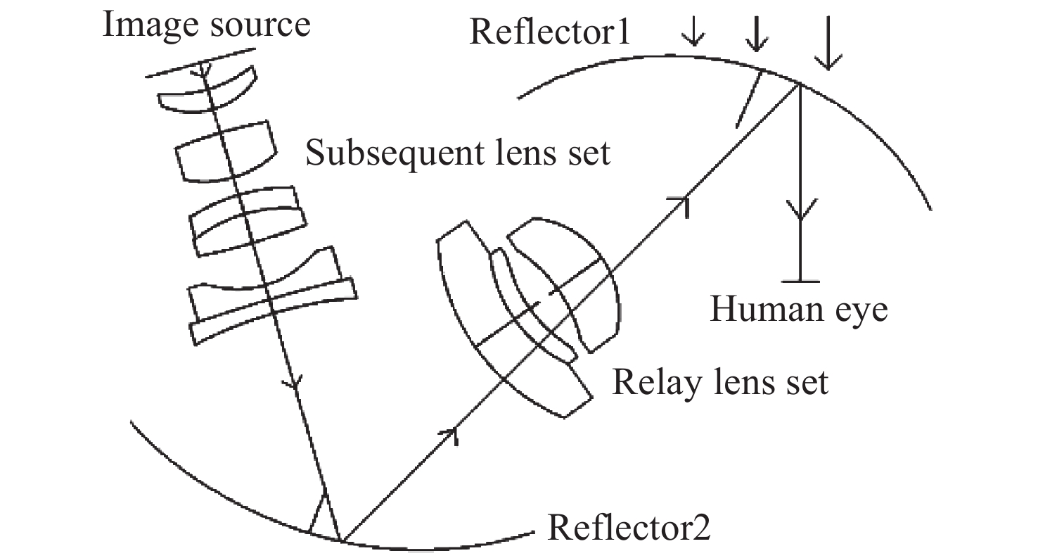
  • 图 1  离轴双反射式非对称光学系统单目一般结构示意图

    Figure 1.  Schematic diagram of monocular general structure of off-axis dual reflection non-symmetric optical system

    图 2  三反射镜非对称光学系统的结构控制示意图

    Figure 2.  Schematic diagram of structure control of non-symmetrical optical system with three mirrors

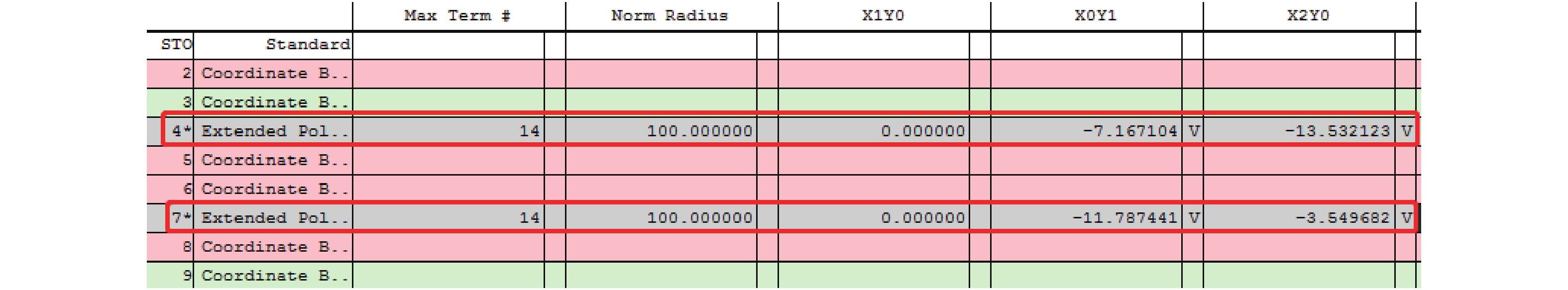
    图 3  双反射镜非对称光学系统的自由曲面参数设置

    Figure 3.  Free-form surface parameter setting of the dual mirror non-symmetric optical system

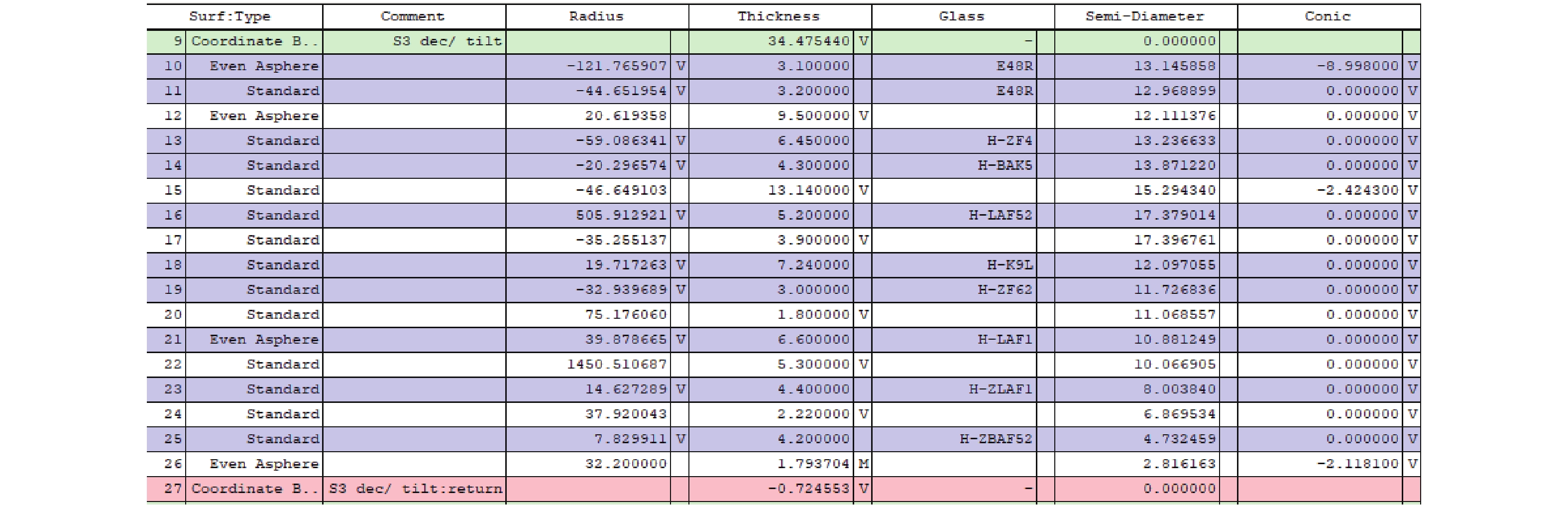
    图 4  双反射镜非对称光学系统的后继透镜组参数设置

    Figure 4.  Parameter setting of the subsequent lens group of the dual mirror non-symmetric optical system

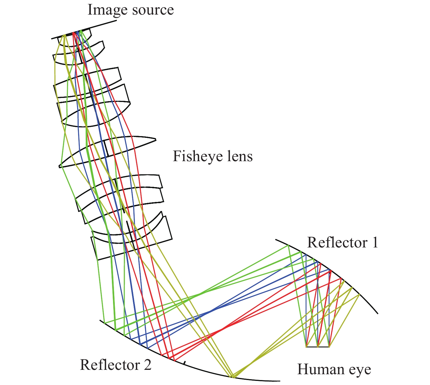
    图 5  双反射镜非对称光学系统的光路示意图

    Figure 5.  Schematic diagram of optical path of dual mirror non-symmetric optical system

    图 6  双反射镜非对称光学系统的MTF曲线图

    Figure 6.  MTF graphs of dual mirror non-symmetric optical system
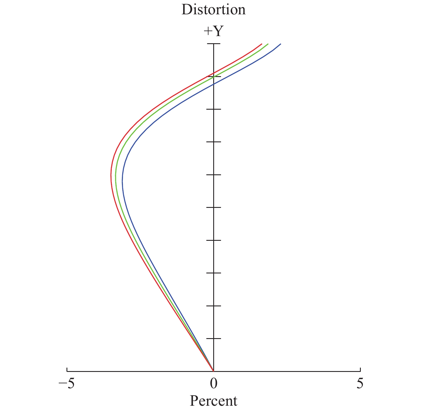
    图 7  双反射镜非对称光学系统的畸变图

    Figure 7.  Distortion diagram of dual mirror non-symmetric optical system
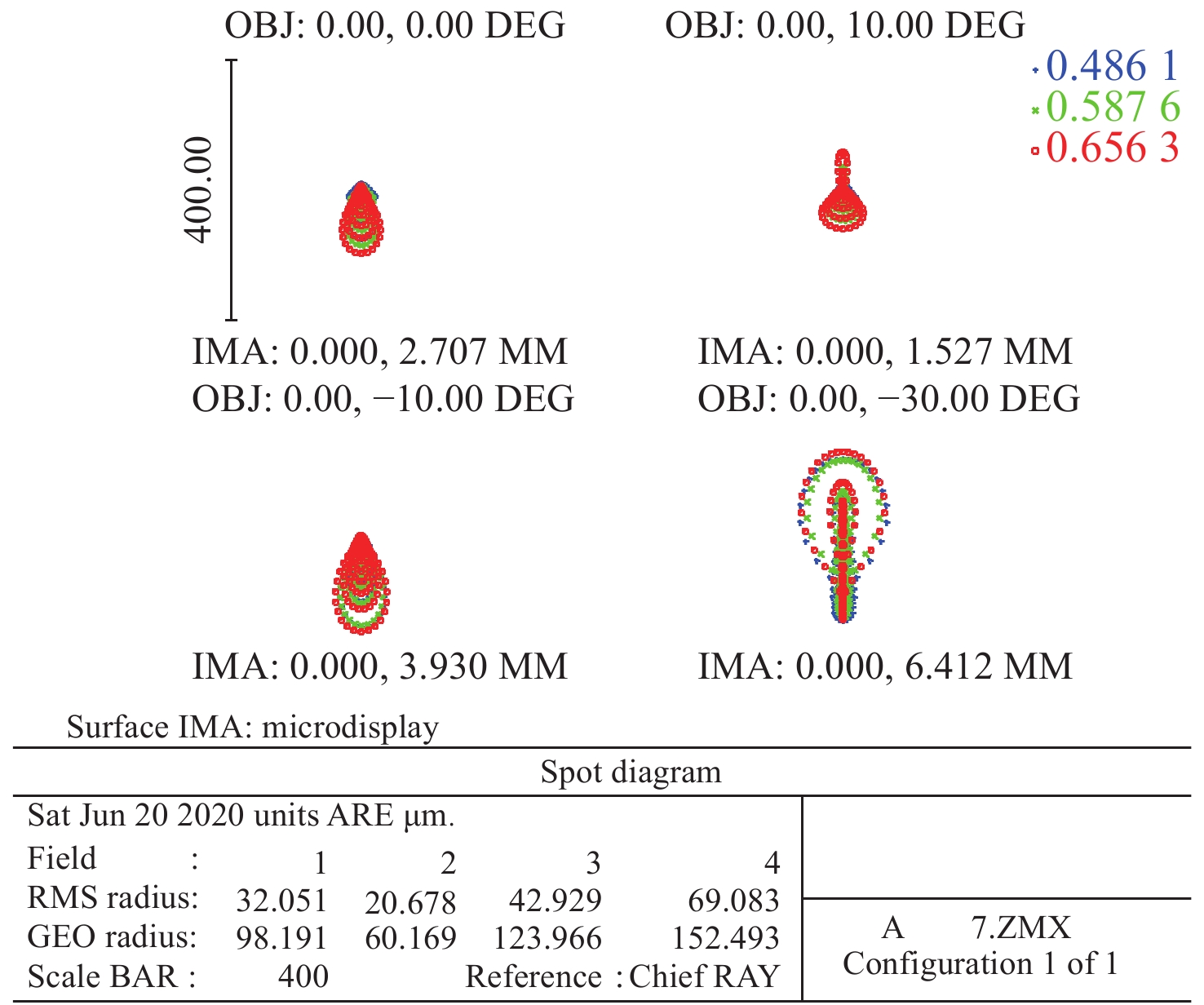
    图 8  双反射镜非对称光学系统的点列图

    Figure 8.  Spot diagram of a double mirror non-symmetric optical system

    表  1  三反射镜非对称光学系统的结构控制宏语言与注解

    Table  1.   Control macro language and annotation of non-symmetric optical system structure with three mirror

    ZPLannotation
    !threemirror.zplZPLXX.zpl
    !
    nfield=NFLD ()Number of fields
    maxfield=MAXF ()Maximum half angle of view
    IF(Maxfield==0.0)
    THEN Maxfield=1.0;
    Avoid errors that divide by zero
    ! 面的个数
    n==pvhx ()Take the value of Hx to n
    ! field
    i=pvhy ()Take the value of Hy to i
    ! 子午或弧矢
    j=pvpy ()Take the value of Py to j
    hx=FLDX(i)/maxfieldHx= field of view (x direction) / maximum field of view
    hy=FLDY(i)/MaxfieldHy= field of view (y direction) / maximum field of view
    PRINT “Field number”, i
    RAYTRACE hx, hy, 0, j, PWAV ()Ray tracing
    PRINT “X-field angle:”, FLDX(i),
    Y-field angle:”, FLDY(i)
    PRINT “X-chief ray:”, RAGX(n),
    Y-chief ray:”, RAGY(n),
    Z-chief ray:”, RAGZ(n)
    Spherical coordinate position at the ray cutoff
    PRINT
    OPTRETURN 0, RAGY(n)
    OPTRETURN 1, RAGZ(n)Return value
    PRINT “All Done!”
    下载: 导出CSV

    表  2  三反射镜非对称光学系统的部分ZPL调用方式

    Table  2.   Partial ZPL calling method of three mirror asymmetric optical system

    Oper#Op1Op2HxHyPxPyTargetWeight
    1 BLNK 1 field of view meridian upper edge of the intersection of light and face 1
    2 ZPLM 11 0 1 1 0 1 0 0
    3 ZPLM 11 1
    4 BLNK 1 field of view meridian upper edge of the intersection of light and face 2
    5 ZPLM 12 0 3 1 0 1 0 0
    6 ZPLM 12 1
    7 BLNK 1 field of view meridian edge light and face 3 intersection
    8 ZPLM 12 0 6 1 0 −1 0 0
    9 ZPLM 12 1
    10 BLNK Solving straight line
    11 DIFF 6 3
    12 DIFF 5 2
    13 BLNK Solving slope k0
    14 DIVI 12 11
    15 BLNK The distance between the line and the light on the meridian of the field of view
    16 PROD 14 9
    17 PROD 14 3
    18 DIFF 16 17
    19 SUMM 2 18
    20 DIFF 8 19
    21 OPLT 20 250 0.1
    22 OPGT 20 25 0.1
    下载: 导出CSV

    表  3  eMagin公司的AMOLED规格参数

    Table  3.   Specifications of AMOLED produced by eMagin

    ItemParameter
    Pixel size/μm 9.6×9.6
    Resolution ratio 1 920×1 200
    Visible area/mm 18.7×11.75 (0.856 inch)
    The white light brightness/(cd·m−2) >150
    Contrast >1000:1
    Refresh rate/Hz 30~85
    Power consumption <350 mW(150 cd/m2)
    Weight/g <3
    下载: 导出CSV
  • [1] 夏振平, 胡伏原, 程成, 等. 基于视觉空间定向理论的虚拟现实空间重构[J]. 液晶与显示, 2019, 34(2): 215-219.

    XIA ZH P, HU F P, CHENG CH, et al. Virtual reality space reconstruction based on visual space orientation theory[J]. Chinese Journal of Liquid Crystals and Displays, 2019, 34(2): 215-219. (in Chinese)
    [2] 王士铭, 程德文, 黄一帆, 等. 大视场高分辨率光学拼接头盔显示器的设计[J]. 激光与光电子学进展,2018,55(6):364-369.

    WANG SH M, CHENG D W, HUANG Y F, et al. Design of wide FOV optical-tiled head-mounted display with high-resolution[J]. Laser &Optoelectronics Progress, 2018, 55(6): 364-369. (in Chinese)
    [3] 程德文, 王涌天, 常军, 等. 轻型大视场自由曲面棱镜头盔显示器的设计[J]. 红外与激光工程,2007,36(3):309-311. doi: 10.3969/j.issn.1007-2276.2007.03.006

    CHENG D W, WANG Y T, CHANG J, et al. Design of a lightweight and wide field-of-view HMD system with free-form-surface prism[J]. Infrared and Laser Engineering, 2007, 36(3): 309-311. (in Chinese) doi: 10.3969/j.issn.1007-2276.2007.03.006
    [4] 徐越, 范君柳, 孙文卿, 等. 基于全息波导的增强现实头盔显示器研究进展[J]. 激光杂志,2019,40(1):11-17.

    XU Y, FAN J L, SUN W Q, et al. Research progress of augmented reality head-mounted display based on holographic waveguide[J]. Laser Journal, 2019, 40(1): 11-17. (in Chinese)
    [5] 刘奡, 张宇宁, 沈忠文, 等. 全息波导显示系统的实现与优化[J]. 光学学报,2017,37(5):0523003. doi: 10.3788/AOS201737.0523003

    LIU A, ZHANG Y N, SHEN ZH W, et al. Realization and optimization of holographic waveguide display system[J]. Acta Optica Sinica, 2017, 37(5): 0523003. (in Chinese) doi: 10.3788/AOS201737.0523003
    [6] 相广鑫, 郭岩, 李文强, 等. L型全息波导构型设计[J]. 电光与控制,2017,24(3):89-92.

    XIANG G X, GUO Y, LI W Q, et al. Design of a holographic waveguide with L configuration[J]. Electronics Optics &Control, 2017, 24(3): 89-92. (in Chinese)
    [7] 何丽鹏, 曾振煌, 林峰. 折/反射式离轴头盔显示器光学系统设计[J]. 激光与光电子学进展,2017,54(12):122201.

    HE L P, ZENG ZH H, LIN F. Optical design of catadioptric off-axis helmet-mounted display[J]. Laser &Optoelectronics Progress, 2017, 54(12): 122201. (in Chinese)
    [8] 刘军, 黄玮. 反射式自由曲面头盔显示器光学系统设计[J]. 红外与激光工程,2016,45(10):1018001. doi: 10.3788/IRLA201645.1018001

    LIU J, HUANG W. Optical system design of reflective head mounted display using freeform surfaces[J]. Infrared and Laser Engineering, 2016, 45(10): 1018001. (in Chinese) doi: 10.3788/IRLA201645.1018001
    [9] 何子清, 葛超, 王春阳. 基于最小二乘配置的光学镜头畸变校正方法[J]. 液晶与显示, 2019, 34(3): 302-308.

    HE Z Q, GE CH, WANG CH Y. Optical lens distortion correction method based on least square configuration[J]. Chinese Journal of Liquid Crystals and Displays, 2019, 34(3): 302-308. (in Chinese)
    [10] 周鑫, 肖锡晟, 孙胜利. 自由曲面在离轴光学系统中的应用[J]. 红外,2017,38(3):6-11, 16. doi: 10.3969/j.issn.1672-8785.2017.03.002

    ZHOU X, XIAO X SH, SUN SH L. Application of free-form surface in off-axis optical systems[J]. Infrared, 2017, 38(3): 6-11, 16. (in Chinese) doi: 10.3969/j.issn.1672-8785.2017.03.002
    [11] 庞志海, 樊学武, 马臻, 等. 自由曲面校正光学系统像差的研究[J]. 光学学报,2016,36(5):0522001. doi: 10.3788/AOS201636.0522001

    PANG ZH H, FAN X W, MA ZH, et al. Free-form optical elements corrected aberrations of optical system[J]. Acta Optica Sinica, 2016, 36(5): 0522001. (in Chinese) doi: 10.3788/AOS201636.0522001
    [12] TSOU B H. System design considerations for a visually coupled system[J]. The Infrared and Electro-Optics Systems Handbook, 1993, 8: 515-540.
    [13] 孟祥翔, 刘伟奇, 张大亮, 等. 双自由曲面大视场头盔显示光学系统设计[J]. 红外与激光工程,2016,45(4):0418004. doi: 10.3788/irla201645.0418004

    MENG X X, LIU W Q, ZHANG D L, et al. Design of wide field-of-view head-mounted display optical system with double freeform surfaces[J]. Infrared and Laser Engineering, 2016, 45(4): 0418004. (in Chinese) doi: 10.3788/irla201645.0418004
    [14] 李华. 头盔显示器光学系统关键技术研究[D]. 长春: 中国科学院研究生院(长春光学精密机械与物理研究所), 2015.

    LI H. Research on key technologies of optical system of helmet-mounted display[D]. Changchun: Changchun Institute of Optics, Fine Mechanics and Physics, Chinese Academy of Sciences, 2015. (in Chinese)
    [15] 张春燕, 陈文栋, 季渊, 等. 基于OLED微显示器的原子扫描控制器设计[J]. 液晶与显示, 2019, 34(4): 395-401.

    ZHANG CH Y, CHEN W D, JI Y, et al. Design of atomic scan controller based on OLED microdisplay[J]. Chinese Journal of Liquid Crystals and Displays, 2019, 34(4): 395-401. (in Chinese)
    [16] 解红军, 张小宝. 一种针对AMOLED器件劣化的电学补偿技术[J]. 液晶与显示, 2019, 34(4): 335-341.

    XIE H J, ZHANG X B. Electronic-compensation technique for improving the degradation of AMOLED Devices[J]. Chinese Journal of Liquid Crystals and Displays, 2019, 34(4): 335-341. (in Chinese)
  • 期刊类型引用(2)

    1. 李政昊,吕枭,李寰,成龙,周文超,吴一辉. ICP快速大面积制备三维内部联通蜂窝状微孔阵列. 光学精密工程. 2023(15): 2227-2235 . 百度学术
    2. 吴绍华,黄攀,赵劲松,赵跃进,郑丽和,董汝昆. 三温区梯度化学气相沉积ZnS制备. 红外与激光工程. 2021(10): 180-185 . 百度学术

    其他类型引用(3)

  • 加载中
图(8) / 表(3)
计量
  • 文章访问数:  2264
  • HTML全文浏览量:  760
  • PDF下载量:  178
  • 被引次数: 5
出版历程
  • 收稿日期:  2019-09-25
  • 修回日期:  2019-11-20
  • 刊出日期:  2020-08-01

目录

/

返回文章
返回