Defects- and interface-enhanced Raman scattering in low-dimensional optoelectronic materials
-
摘要: 近年来,一系列新型低维光电材料相继涌现,展现出优异的性能。这些光电材料与表面增强拉曼散射(SERS)技术相结合,显示出巨大的应用潜力,有望成为高灵敏SERS活性基底。缺陷与界面调控是低维光电材料SERS应用的重要策略,本文将重点介绍新型低维光电材料缺陷与界面增强拉曼散射的种类和增强机理。通过对缺陷与界面增强拉曼散射的应用和研究前景的展望,启发人们对SERS研究的再思考和再认识。Abstract: In recent years, a series of new low-dimensional optoelectronic materials with excellent properties have emerged. Combined with surface-enhanced Raman scattering (SERS) technology, they show great application potential and are expected to become highly sensitive SERS substrates. Defects and interface regulation of low-dimensional optoelectronic materials are important strategies for their applications in SERS technology. In this paper, the types and enhancement mechanisms of defects- and interface-enhanced Raman scattering in new low-dimensional optoelectronic materials are introduced. By looking forward to the application and research prospect of defects- and interface-enhanced Raman scattering, this work might inspire people to reconsider and further understand the study of SERS.
-
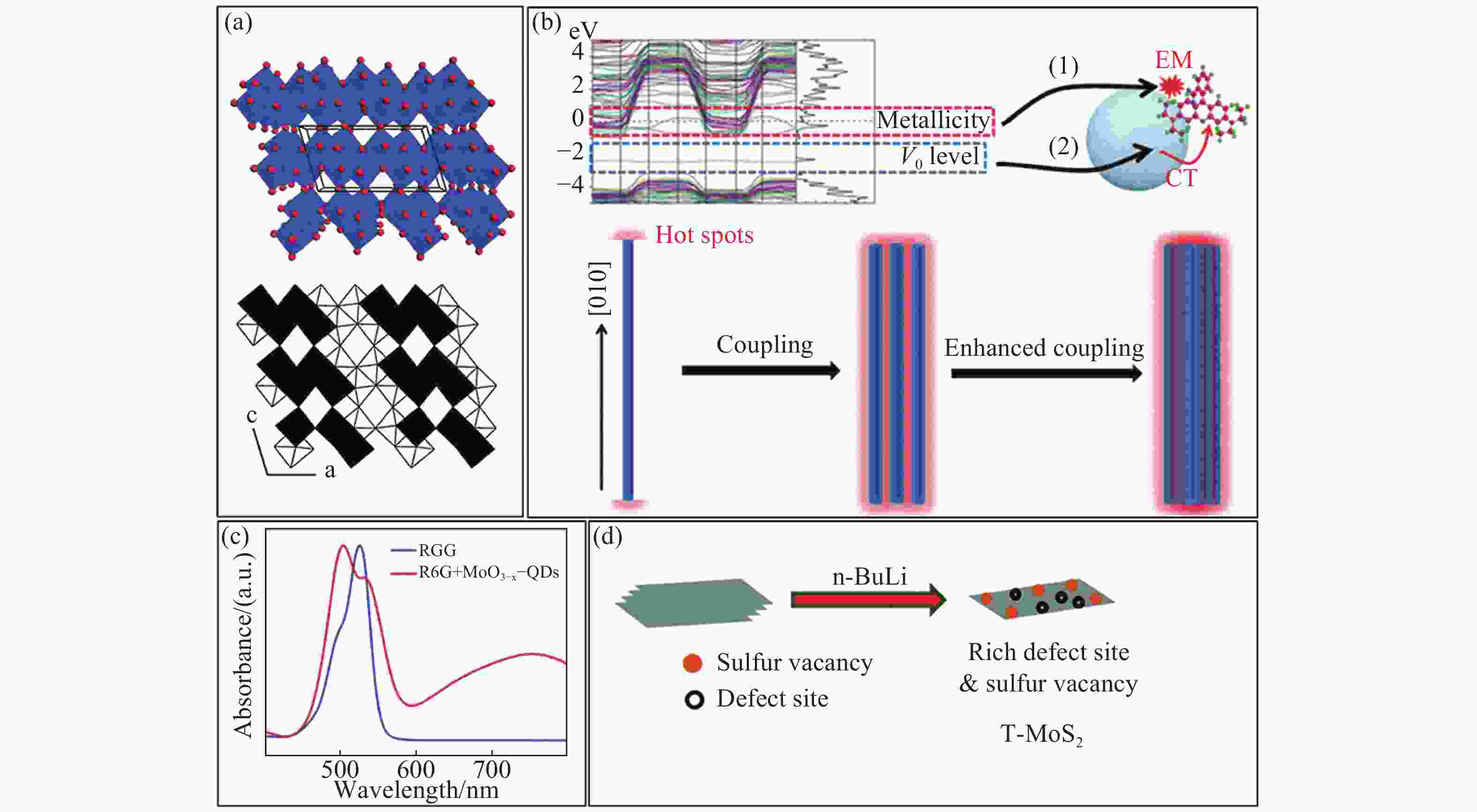
图 4 (a)本身具有周期性氧空位的二氧化钒纳米片的晶体结构示意图[25];(b)合成富含氧空位的氧化钨纳米线利用电荷转移和等离激元共振协同增强拉曼散射的示意图[26];(c)合成富含氧空位的氧化钼量子点与吸附分子体系的吸收光谱[28];(d)锂溶液直接剥离富含硫空位的二维硫化钼示意图[31]
Figure 4. (a) Schematic diagram of crystal structures of vanadium dioxide nanosheets with periodic oxygen vacancies[25]; (b) schematic diagram of enhanced Raman scattering caused by the synergistic effect of surface plasmon resonance coupling and charge transfer in tungsten oxide nanowires with oxygen vacancies[26]; (c) UV-vis spectra of adsorbed molecules and molybdenum trioxide quantum dots with oxygen vacancies[28]; (d) schematic diagram of lithium-exfoliated molybdenum disulfide with suffur vacancies[31]
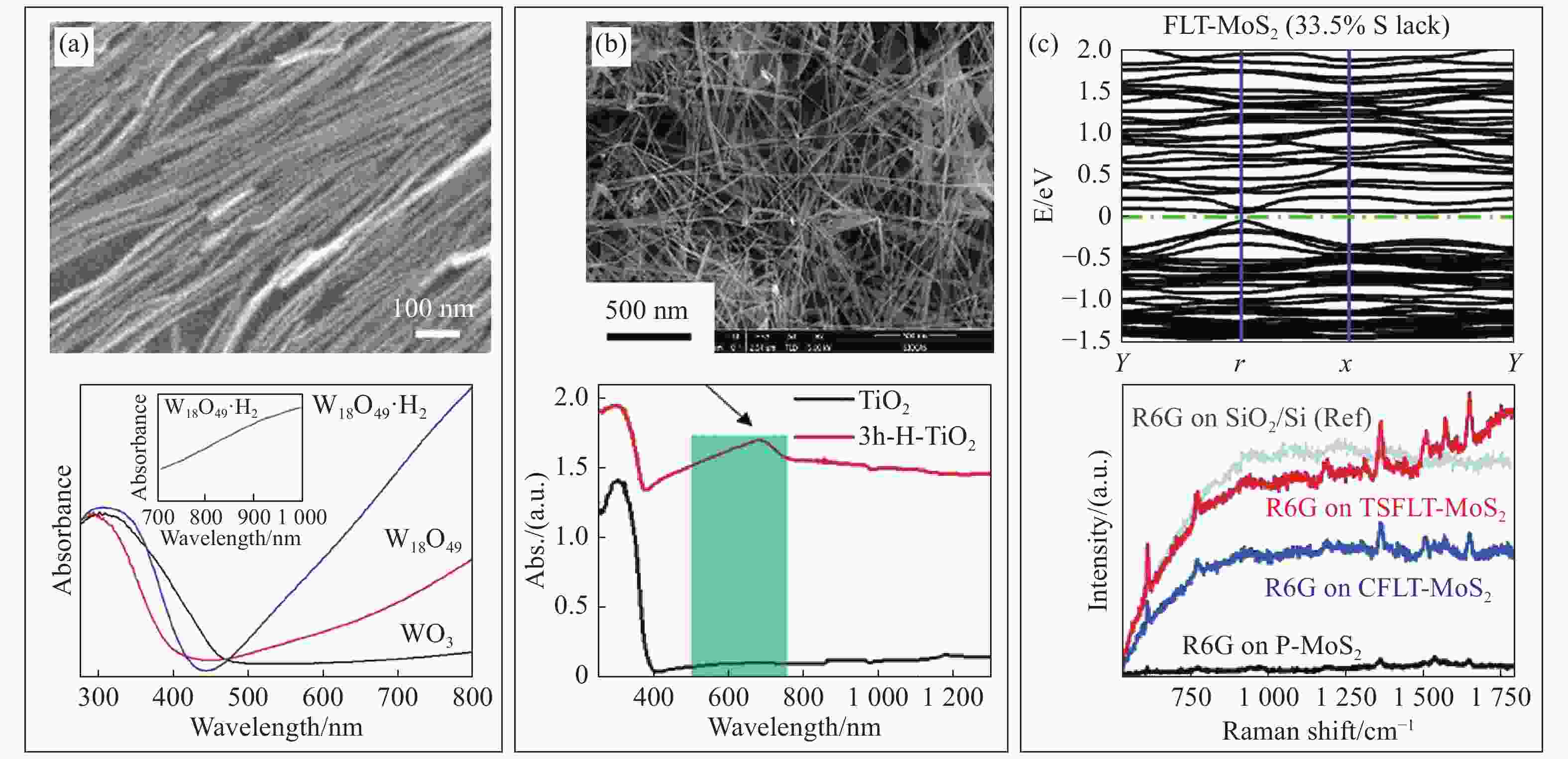
图 5 (a)退火形成富含氧空位的氧化钨纳米线的扫描电子显微镜图像(上)和吸收光谱(下)[29];(b)水热反应制造富含氧空位的二氧化钛纳米线的扫描电子显微镜图像(上)和吸收光谱(下)[30];(c)激光诱导富含硫空位的单层硫化钼的能带(上)和增强拉曼散射谱图(下)[32]
Figure 5. (a) Scanning electron microscopy image (top) and UV-vis spectra (bottom) of tungsten oxide nanowires rich in oxygen vacancies formed by annealing[29]; (b) scanning electron microscopy image (top) and UV-vis spectra (bottom) of titanium dioxide nanowires rich in oxygen vacancies produced by a hydrothermal reaction[30]; (c) bandgaps (top) and surface-enhanced Raman spectra (bottom) of femtosecond laser-treated molybdenum sulfide rich in sulfur vacancies[32]
图 6 (a)石墨烯与二硒化钨异质结利用层间电荷转移实现增强拉曼散射的示意图[33];(b)富含氧空位的氧化钨与单层硫化钼异质结利用层间电荷转移和多种激子共振实现增强拉曼散射的示意图[34-35];(c)单层硫化钼和二硒化锡异质结利用非辐射能量转移效应增强拉曼散射的示意图[36-37];(d)外加磁场下形成的石墨烯和罗丹明6G三明治结构的示意图[38]
Figure 6. Schematic diagram of enhanced Raman scattering caused by (a) the interlayer charge transfer in the graphene and tungsten disulfide heterojunction[33], (b) the interlayer charge transfer and multiple exciton resonances in tungsten oxide rich in oxygen vacancies and with a monolayer molybdenum sulfide heterojunction[34-35], and (c) nonradiative energy transfer effect in monolayer molybdenum sulfide and tin diselenide heterostructure[36-37]; (d) pressure-induced surface enhanced Raman scattering in graphene-molecule-graphene sandwich structures under an external magnetic field[38]
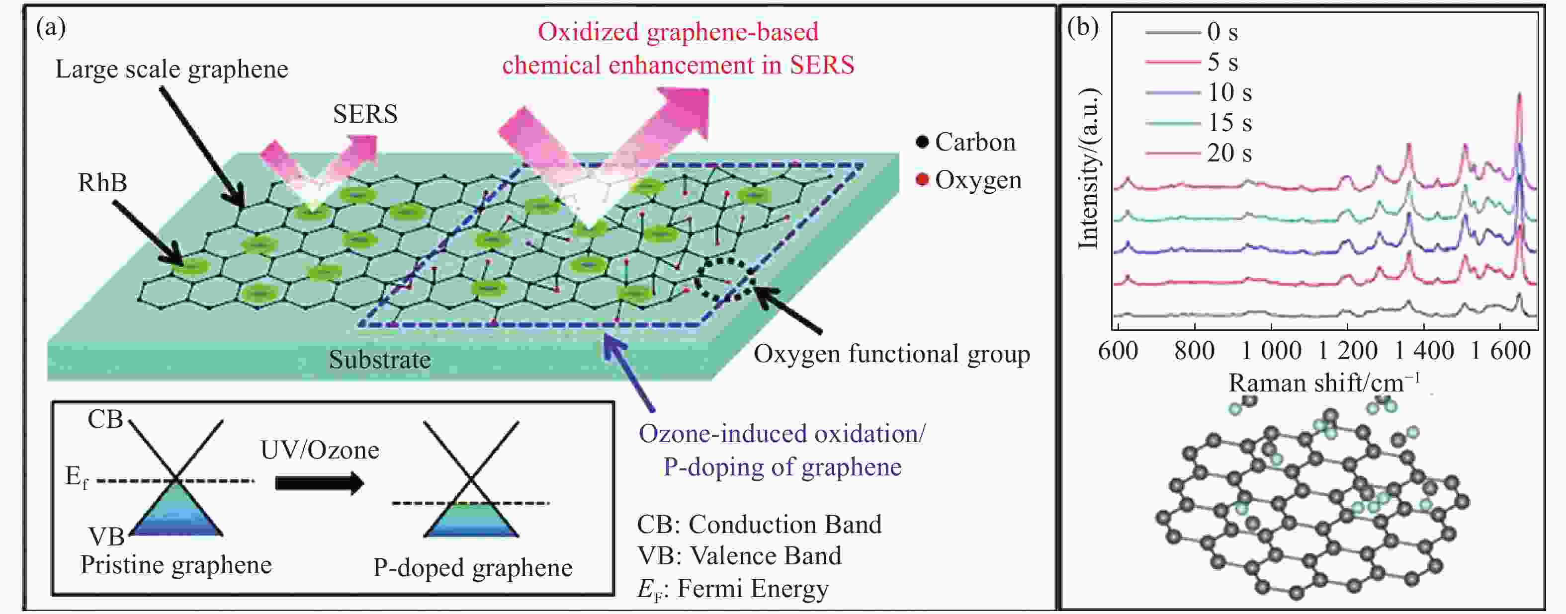
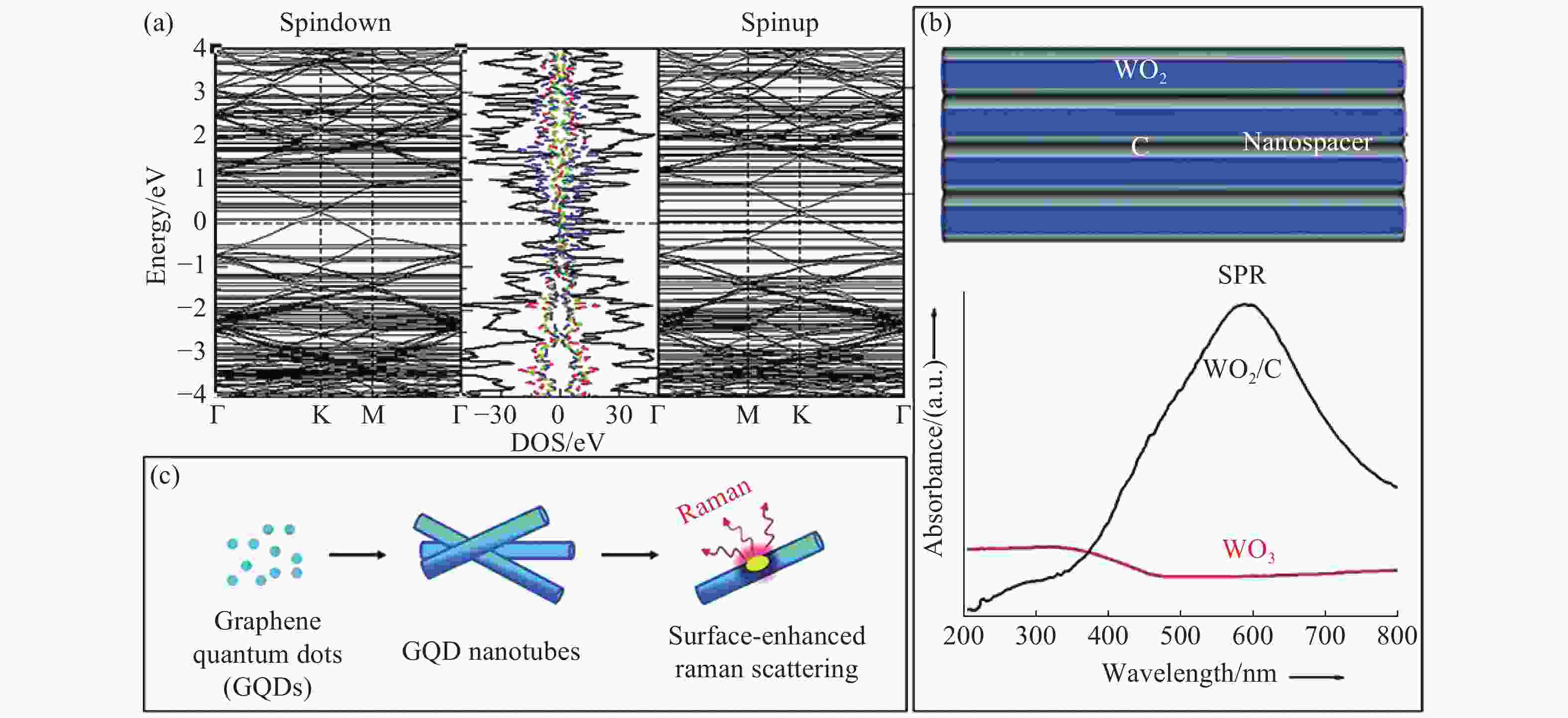
图 7 (a)硫化钼量子点和二维还原氧化石墨烯界面结构的能带和态密度[39];(b)混杂二氧化钨和碳纳米线束状界面结构的吸收光谱[40];(c)石墨烯量子点形成一维纳米管和其表面增强拉曼散射的示意图[41]
Figure 7. (a) The energy band and density of the states of the interface structure between a molybdenum disulfide quantum dot and reduced graphene oxide[39]; (b) UV-vis spectra of hybrid tungsten dioxide/carbon ultrathin nanowire beams[40]; (c) scheme of the fabrication of graphene-quantum-dot assembled nanotubes and their SERS function[41]
-
[1] FLEISCHMANN M, HENDRA P J, MCQUILLAN A J. Raman spectra of pyridine adsorbed at a silver electrode[J]. Chemical Physics Letters, 1974, 26(2): 163-166. doi: 10.1016/0009-2614(74)85388-1 [2] JEANMAIRE D L, VAN DUYNE R P. Surface raman spectroelectrochemistry: Part I. Heterocyclic, aromatic, and aliphatic amines adsorbed on the anodized silver electrode[J]. Journal of Electroanalytical Chemistry and Interfacial Electrochemistry, 1977, 84(1): 1-20. doi: 10.1016/S0022-0728(77)80224-6 [3] NIE SH M, EMORY S R. Probing single molecules and single nanoparticles by surface-enhanced Raman scattering[J]. Science, 1997, 275(5303): 1102-1106. doi: 10.1126/science.275.5303.1102 [4] HOU X Y, ZHANG X Y, MA Q W, et al. Alloy engineering in few-layer manganese phosphorus trichalcogenides for surface-enhanced Raman scattering[J]. Advanced Functional Materials, 2020, 30(12): 1910171. doi: 10.1002/adfm.201910171 [5] TAO L, CHEN K, CHEN Z F, et al. 1T′ transition metal telluride atomic layers for plasmon-free SERS at femtomolar levels[J]. Journal of the American Chemical Society, 2018, 140(28): 8696-8704. doi: 10.1021/jacs.8b02972 [6] KARTHICK KANNAN P, SHANKAR P, BLACKMAN C, et al. Recent advances in 2D inorganic nanomaterials for SERS sensing[J]. Advanced Materials, 2019, 31(34): 1803432. doi: 10.1002/adma.201803432 [7] ALESSANDRI I, LOMBARDI J R. Enhanced Raman scattering with dielectrics[J]. Chemical Reviews, 2016, 116(24): 14921-14981. doi: 10.1021/acs.chemrev.6b00365 [8] LOMBARDI J R. The theory of surface-enhanced Raman scattering on semiconductor nanoparticles; Toward the optimization of SERS sensors[J]. Faraday Discussions, 2017, 205: 105-120. doi: 10.1039/C7FD00138J [9] 程光煦. 也谈光散射增强[J]. 光散射学报,2016,28(4):374-390.CHENG G X. Also talking about the enhanced in light scattering[J]. The Journal of Light Scattering, 2016, 28(4): 374-390. (in Chinese) [10] HU Z H, WU ZH T, HAN C, et al. Two-dimensional transition metal dichalcogenides: Interface and defect engineering[J]. Chemical Society Reviews, 2018, 47(9): 3100-3128. doi: 10.1039/C8CS00024G [11] LING X, XIE L M, FANG Y, et al. Can graphene be used as a substrate for Raman enhancement?[J]. Nano Letters, 2010, 10(2): 553-561. doi: 10.1021/nl903414x [12] HUH S, PARK J, KIM Y S, et al. UV/ozone-oxidized large-scale graphene platform with large chemical enhancement in surface-enhanced Raman scattering[J]. ACS Nano, 2011, 5(12): 9799-9806. doi: 10.1021/nn204156n [13] MAO H Y, WANG R, ZHONG J Q, et al. Mildly O2 plasma treated CVD graphene as a promising platform for molecular sensing[J]. Carbon, 2014, 76: 212-219. doi: 10.1016/j.carbon.2014.04.070 [14] SUN L F, HU H L, ZHAN D, et al. Plasma modified MoS2 nanoflakes for surface enhanced raman scattering[J]. Small, 2014, 10(6): 1090-1095. doi: 10.1002/smll.201300798 [15] YU X X, LIN K, QIU K Q, et al. Increased chemical enhancement of Raman spectra for molecules adsorbed on fluorinated reduced graphene oxide[J]. Carbon, 2012, 50(12): 4512-4517. doi: 10.1016/j.carbon.2012.05.033 [16] LV R T, LI Q, BOTELLO-MÉNDEZ A R, et al. Nitrogen-doped graphene: Beyond single substitution and enhanced molecular sensing[J]. Scientific Reports, 2012, 2(1): 586. doi: 10.1038/srep00586 [17] FENG S M, CRISTINA DOS SANTOS M, CARVALHO B R, et al. Ultrasensitive molecular sensor using N-doped graphene through enhanced Raman scattering[J]. Science Advances, 2016, 2(7): e1600322. doi: 10.1126/sciadv.1600322 [18] REN P Y, PU E Q, LIU D B, et al. Fabrication of nitrogen-doped graphenes by pulsed laser deposition and improved chemical enhancement for Raman spectroscopy[J]. Materials Letters, 2017, 204: 65-68. doi: 10.1016/j.matlet.2017.05.124 [19] SUN Y S, LIN C F, LUO S T. Two-dimensional nitrogen-enriched carbon nanosheets with surface-enhanced raman scattering[J]. The Journal of Physical Chemistry C, 2017, 121(27): 14795-14802. doi: 10.1021/acs.jpcc.7b02913 [20] DAS R, PARVEEN S, BORA A, et al. Origin of high photoluminescence yield and high SERS sensitivity of nitrogen-doped graphene quantum dots[J]. Carbon, 2020, 160: 273-286. doi: 10.1016/j.carbon.2020.01.030 [21] HU L, XU ZH Y, LONG F CH, et al. Direct bandgap opening in sodium-doped antimonene quantum dots: an emerging 2D semiconductor[J]. Materials Horizons, 2020, 7(6): 1588-1596. doi: 10.1039/D0MH00440E [22] CONG SH, YUAN Y Y, CHEN ZH G, et al. Noble metal-comparable SERS enhancement from semiconducting metal oxides by making oxygen vacancies[J]. Nature Communications, 2015, 6(1): 7800. doi: 10.1038/ncomms8800 [23] HOU X Y, FAN X C, WEI PH, et al. Planar transition metal oxides SERS chips: a general strategy[J]. Journal of Materials Chemistry C, 2019, 7(36): 11134-11141. doi: 10.1039/C9TC03195B [24] HOU X Y, LUO X G, FAN X C, et al. Plasmon-coupled charge transfer in WO3-X semiconductor nanoarrays: toward highly uniform silver-comparable SERS platforms[J]. Physical Chemistry Chemical Physics, 2019, 21(5): 2611-2618. doi: 10.1039/C8CP07305H [25] MIAO P, WU J, DU Y CH, et al. Phase transition induced Raman enhancement on vanadium dioxide (VO2) nanosheets[J]. Journal of Materials Chemistry C, 2018, 6(40): 10855-10860. doi: 10.1039/C8TC04269A [26] LIU W, BAI H, LI X SH, et al. Improved surface-enhanced raman spectroscopy sensitivity on metallic tungsten oxide by the synergistic effect of surface plasmon resonance coupling and charge transfer[J]. The Journal of Physical Chemistry Letters, 2018, 9(14): 4096-4100. doi: 10.1021/acs.jpclett.8b01624 [27] YU H H, ZHUANG ZH F, LI D L, et al. Photo-induced synthesis of molybdenum oxide quantum dots for surface-enhanced Raman scattering and photothermal therapy[J]. Journal of Materials Chemistry B, 2020, 8(5): 1040-1048. doi: 10.1039/C9TB02102G [28] ZHANG J J, PAN Y M, CHEN Y F, et al. Plasmonic molybdenum trioxide quantum dots with noble metal-comparable surface enhanced Raman scattering[J]. Journal of Materials Chemistry C, 2018, 6(9): 2216-2220. doi: 10.1039/C7TC04807F [29] WANG X Y, LI J, SHEN Y H, et al. An assembled ordered W18O49 nanowire film with high SERS sensitivity and stability for the detection of RB[J]. Applied Surface Science, 2020, 504: 144073. doi: 10.1016/j.apsusc.2019.144073 [30] YANG L L, PENG Y S, YANG Y, et al. Green and sensitive flexible semiconductor SERS substrates: hydrogenated black TiO2 nanowires[J]. ACS Applied Nano Materials, 2018, 1(9): 4516-4527. doi: 10.1021/acsanm.8b00796 [31] ANBAZHAGAN R, VADIVELMURUGAN A, TSAI H C, et al. Surface-enhanced Raman scattering of alkyne-conjugated MoS2: a comparative study between metallic and semiconductor phases[J]. Journal of Materials Chemistry C, 2018, 6(5): 1071-1082. doi: 10.1039/C7TC03682E [32] ZUO P, JIANG L, LI X, et al. Enhancing charge transfer with foreign molecules through femtosecond laser induced MoS2 defect sites for photoluminescence control and SERS enhancement[J]. Nanoscale, 2019, 11(2): 485-494. doi: 10.1039/C8NR08785G [33] TAN Y, MA L N, GAO Z B, et al. Two-dimensional heterostructure as a platform for surface-enhanced raman scattering[J]. Nano Letters, 2017, 17(4): 2621-2626. doi: 10.1021/acs.nanolett.7b00412 [34] LI M Z, FAN X C, GAO Y M, et al. W18O49/monolayer MoS2 heterojunction-enhanced raman scattering[J]. The Journal of Physical Chemistry Letters, 2019, 10(14): 4038-4044. doi: 10.1021/acs.jpclett.9b00972 [35] SEO J, LEE J, KIM Y, et al. Ultrasensitive plasmon-free surface-enhanced raman spectroscopy with femtomolar detection limit from 2D van der waals heterostructure[J]. Nano Letters, 2020, 20(3): 1620-1630. doi: 10.1021/acs.nanolett.9b04645 [36] DANDU M, WATANABE K, TANIGUCHI T, et al. Spectrally tunable, large raman enhancement from nonradiative energy transfer in the van der waals heterostructure[J]. ACS Photonics, 2020, 7(2): 519-527. doi: 10.1021/acsphotonics.9b01648 [37] REN P Y, ZHOU W CH, REN X P, et al. Improved surface-enhanced Raman scattering (SERS) sensitivity to molybdenum oxide nanosheets via the lightning rod effect with application in detecting methylene blue[J]. Nanotechnology, 2020, 31(22): 224002. doi: 10.1088/1361-6528/ab758b [38] LEE Y, KIM H, LEE J B, et al. Pressure-induced chemical enhancement in Raman scattering from graphene-Rhodamine 6G-graphene sandwich structures[J]. Carbon, 2015, 89: 318-327. doi: 10.1016/j.carbon.2015.03.065 [39] WU D, CHEN J L, RUAN Y E, et al. A novel sensitive and stable surface enhanced Raman scattering substrate based on a MoS2 quantum dot/reduced graphene oxide hybrid system[J]. Journal of Materials Chemistry C, 2018, 6(46): 12547-12554. doi: 10.1039/C8TC05151H [40] HE CH Y, BAI H, YI W C, et al. A highly sensitive and stable SERS substrate using hybrid tungsten dioxide/carbon ultrathin nanowire beams[J]. Journal of Materials Chemistry C, 2018, 6(13): 3200-3205. doi: 10.1039/C8TC00573G [41] CHENG H H, ZHAO Y, FAN Y Q, et al. Graphene-quantum-dot assembled nanotubes: a new platform for efficient Raman enhancement[J]. ACS Nano, 2012, 6(3): 2237-2244. doi: 10.1021/nn204289t [42] LIVINGSTONE R, ZHOU X C, TAMARGO M C, et al. Surface enhanced Raman spectroscopy of pyridine on CdSe/ZnBeSe quantum dots grown by molecular beam epitaxy[J]. The Journal of Physical Chemistry C, 2010, 114(41): 17460-17464. doi: 10.1021/jp105619m [43] QUAGLIANO L G. Observation of molecules adsorbed on III-V semiconductor quantum dots by surface-enhanced Raman scattering[J]. Journal of the American Chemical Society, 2004, 126(23): 7393-7398. doi: 10.1021/ja031640f [44] LOMBARDI J R, BIRKE R L. The theory of surface-enhanced Raman scattering[J]. The Journal of Chemical Physics, 2012, 136(14): 144704. doi: 10.1063/1.3698292 [45] XU H, XIE L M, ZHANG H L, et al. Effect of graphene Fermi level on the Raman scattering intensity of molecules on graphene[J]. ACS Nano, 2011, 5(7): 5338-5344. doi: 10.1021/nn103237x [46] ZHOU C L, SUN L F, ZHANG F Q, et al. Electrical tuning of the sers enhancement by precise defect density control[J]. ACS Applied Materials &Interfaces, 2019, 11(37): 34091-34099. [47] LIN J, YU J, AKAKURU O U, et al. Low temperature-boosted high efficiency photo-induced charge transfer for remarkable SERS activity of ZnO nanosheets[J]. Chemical Science, 2020, 11(35): 9414-9420. doi: 10.1039/D0SC02712J [48] WU H, WANG H, LI G H. Metal oxide semiconductor SERS-active substrates by defect engineering[J]. Analyst, 2017, 142(2): 326-335. doi: 10.1039/C6AN01959E [49] QIU H W, WANG M Q, ZHANG L, et al. Wrinkled 2H-phase MoS2 sheet decorated with graphene-microflowers for ultrasensitive molecular sensing by plasmon-free SERS enhancement[J]. Sensors and Actuators B:Chemical, 2020, 320: 128445. doi: 10.1016/j.snb.2020.128445 -


 下载:
下载:
