Hybrid graphene/n-GaAs photodiodes with high specific detectivity and high speed
doi: 10.37188/CO.2020-0153
-
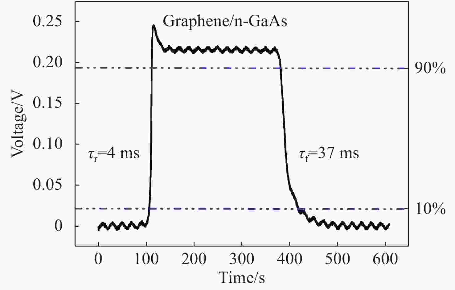
摘要: 混合结构的石墨烯/半导体光电晶体管因其超高的响应度而备受关注。然而,该类光电晶体管通过源-漏电极测试得到的比探测率(D*)容易受到1/f噪声的限制。本文制备了混合结构的石墨烯/GaAs光电探测器,通过源-栅电极测得D*大约为1.82×1011 Jones,与通过源-漏电极测量相比,D*提高了约500倍。这可归因于界面上肖特基势垒对载流子俘获和释放过程的屏蔽作用。此外,探测器的上升时间和下降时间分别是4 ms和37 ms,响应速度相应地提高了2个数量级。该工作为制备高比探测率和高速的光电探测器提供了一种新的思路。Abstract: Hybrid graphene/semiconductor phototransistors have attracted great attention because of their ultrahigh responsivity. However, the specific detectivity (D*) for such hybrid phototransistors obtained from source-drain electrodes is assumed to be 1/f noise. In this paper, D* of ~1.82×10¹¹ Jones was achieved from source-gate electrodes. Compared with the same device which was measured from source-drain electrodes, D* was improved by ~500 times. This could be attributed to the carrier trapping and detrapping processes having been screened by the Schottky barrier at the interface. The rise and decay times were 4 ms and 37 ms, respectively. The temporal response speed also correspondingly improved by ~2 orders of magnitude. This work provides an alternative route toward light photodetectors with high specific detectivity and speed.
-
Key words:
- graphene /
- photodiode /
- specific detectivity /
- response speed
-
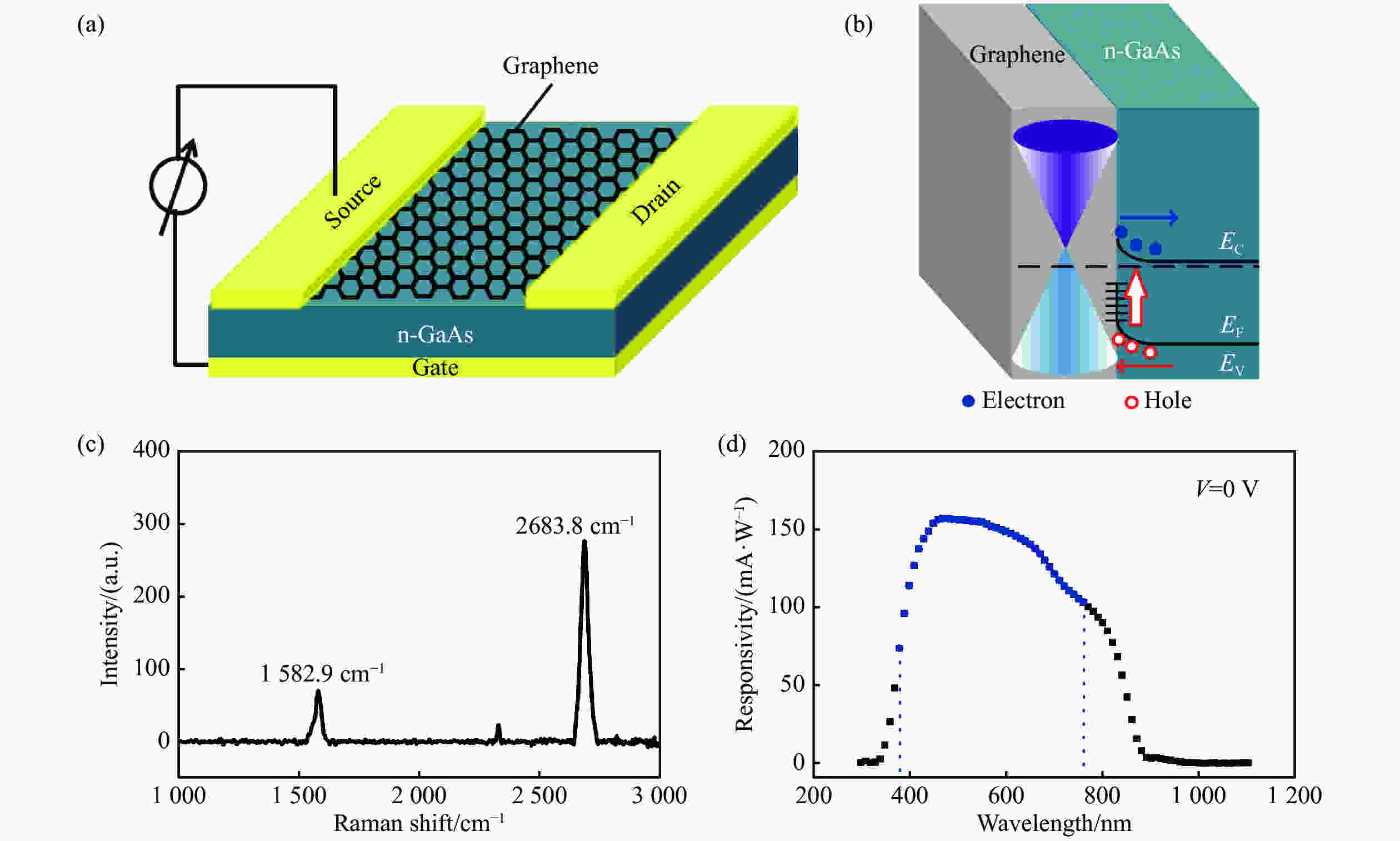
Figure 1. (a) Schematic diagram of the graphene/n-GaAs photodetector. The optical and electrical performances were measured by source-gate electrodes. (b) Energy band diagram of the graphene/n-GaAs heterojunction with the Schottky barrier height ΦB of the graphene/GaAs junction of ~0.7 eV. The interface states are depicted at the interface, illustrating that the carrier trapped photons at the graphene/GaAs interface during carrier transport through the junction. (c) Measurement result of the Raman spectrum of graphene on the GaAs substrate. (d) Spectral response of the photodiode under zero bias voltage.
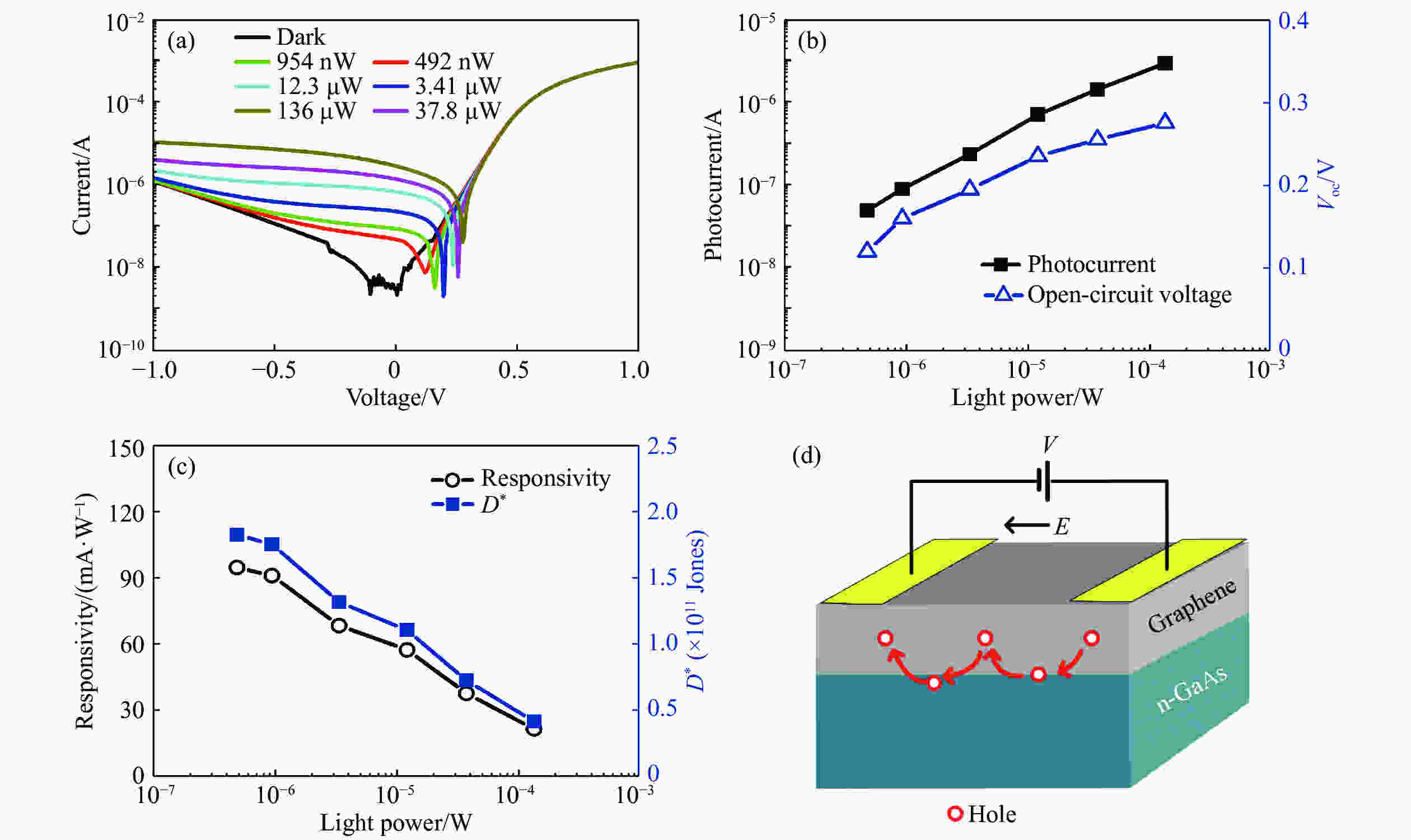
Figure 2. (a) Current versus voltage curves of the device under different light powers. (b) The relationship between photocurrent and photovoltage (Voc) with the incident light’s power in the self-driven mode. (c) Responsivity and D* versus illumination power under a zero bias voltage. (d) Illustration of the carrier trapping and detrapping processes at the interface of the graphene/GaAs interface, which is the main source of 1/f noise.
-
[1] KOPPENS F H L, MUELLER T, AVOURIS P, et al. Photodetectors based on graphene, other two-dimensional materials and hybrid systems[J]. Nature Nanotechnology, 2014, 9(10): 780-793. doi: 10.1038/nnano.2014.215 [2] NAIR R R, BLAKE P, GRIGORENKO A N, et al. Fine structure constant defines visual transparency of graphene[J]. Science, 2008, 320(5881): 1308. doi: 10.1126/science.1156965 [3] GUO X T, WANG W H, NAN H Y, et al. High-performance graphene photodetector using interfacial gating[J]. Optica, 2016, 3(10): 1066-1070. doi: 10.1364/OPTICA.3.001066 [4] GREBENCHUKOV A N, ZAITSEV A D, KHODZITSKY M K. Optically controlled narrowband terahertz switcher based on graphene[J]. Chinese Optics, 2018, 11(2): 166-173. doi: 10.3788/co.20181102.0166 [5] HU A Q, TIAN H J, LIU Q L, et al. Graphene on self-assembled InGaN quantum dots enabling ultrahighly sensitive photodetectors[J]. Advanced Optical Materials, 2019, 7(8): 1801792. doi: 10.1002/adom.201801792 [6] LIU Q L, TIAN H J, LI J W, et al. Hybrid graphene/Cu2O quantum dot photodetectors with ultrahigh responsivity[J]. Advanced Optical Materials, 2019, 7(20): 1900455. doi: 10.1002/adom.201900455 [7] GONG X, TONG M H, XIA Y J, et al. High-detectivity polymer photodetectors with spectral response from 300 nm to 1450 nm[J]. Science, 2009, 325(5948): 1665-1667. doi: 10.1126/science.1176706 [8] WANG G SH, LU H, CHEN D J, et al. High quantum efficiency GaN-based p-i-n ultraviolet photodetectors prepared on patterned sapphire substrates[J]. IEEE Photonics Technology Letters, 2013, 25(7): 652-654. doi: 10.1109/LPT.2013.2248056 [9] BALANDIN A A. Low-frequency 1/f noise in graphene devices[J]. Nature Nanotechnology, 2013, 8(8): 549-555. doi: 10.1038/nnano.2013.144 [10] LU Y H, FENG S R, WU ZH Q, et al. Broadband surface plasmon resonance enhanced self-powered graphene/GaAs photodetector with ultrahigh detectivity[J]. Nano Energy, 2018, 47: 140-149. doi: 10.1016/j.nanoen.2018.02.056 [11] TIAN H J, HU A Q, LIU Q L, et al. Interface-induced high responsivity in hybrid graphene/GaAs photodetector[J]. Advanced Optical Materials, 2020, 8(8): 1901741. doi: 10.1002/adom.201901741 [12] HU W D, LI Q, CHEN X SH, et al. Recent progress on advanced infrared photodetectors[J]. Acta Physica Sinica, 2019, 68(12): 120701. (in Chinese) [13] CHEN Y Y, WANG C H, CHEN G S, et al. Self-powered n-MgxZn1−xO/p-Si photodetector improved by alloying-enhanced piezopotential through piezo-phototronic effect[J]. Nano Energy, 2015, 11: 533-539. doi: 10.1016/j.nanoen.2014.09.037 [14] FAUSKE V T, HUH J, DIVITINI G, et al. In situ heat-induced replacement of GaAs nanowires by Au[J]. Nano Letters, 2016, 16(5): 3051-3057. doi: 10.1021/acs.nanolett.6b00109 [15] ZHANG X T, ZHANG L N, CHAN M S. Doping enhanced barrier lowering in graphene-silicon junctions[J]. Applied Physics Letters, 2016, 108(26): 263502. doi: 10.1063/1.4954799 [16] LI X Q, LIN SH SH, LIN X, et al. Graphene/h-BN/GaAs sandwich diode as solar cell and photodetector[J]. Optics Express, 2016, 24(1): 134-145. doi: 10.1364/OE.24.000134 [17] CANCADO L G, JORIO A, FERREIRA E H M, et al. Quantifying defects in graphene via Raman spectroscopy at different excitation energies[J]. Nano Letters, 2011, 11(8): 3190-3196. doi: 10.1021/nl201432g [18] HAO Y F, WANG Y Y, WANG L, et al. Probing layer number and stacking order of few-layer graphene by Raman spectroscopy[J]. Small, 2010, 6(2): 195-200. doi: 10.1002/smll.200901173 [19] DI BARTOLOMEO A. Graphene Schottky diodes: an experimental review of the rectifying graphene/semiconductor heterojunction[J]. Physics Reports, 2016, 606: 1-58. doi: 10.1016/j.physrep.2015.10.003 [20] TONGAY S, LEMAITRE M, MIAO X, et al. Rectification at graphene-semiconductor interfaces: zero-gap semiconductor-based diodes[J]. Physics Review X, 2012, 2(1): 011002. [21] LIN F, CHEN SH W, MENG J, et al. Graphene/GaN diodes for ultraviolet and visible photodetectors[J]. Applied Physics Letters, 2014, 105(7): 073103. doi: 10.1063/1.4893609 [22] NI ZH Y, MA L L, DU S CH, et al. Plasmonic silicon quantum dots enabled high-sensitivity ultrabroadband photodetection of graphene-based hybrid phototransistors[J]. ACS Nano, 2017, 11(10): 9854-9862. doi: 10.1021/acsnano.7b03569 [23] ZENG L H, WU D, LIN SH H, et al. Controlled synthesis of 2D palladium diselenide for sensitive photodetector applications[J]. Advanced Functional Materials, 2019, 29(1): 1806878. doi: 10.1002/adfm.201806878 [24] MEIRZADEH E, CHRISTENSEN D V, MAKAGON E, et al. Surface pyroelectricity in cubic SrTiO3[J]. Advanced Materials, 2019, 31(44): 1904733. doi: 10.1002/adma.201904733 -


 下载:
下载:


