


Room-temperature terahertz photodetectors based on black arsenic-phosphorus
doi: 10.37188/CO.2020-0175
-
摘要: 由于太赫兹波与众多物质之间存在着丰富的相互作用,太赫兹技术在众多领域均有应用需求。因此,基于独特物理机制和优异材料特性的高灵敏度、便携式太赫兹探测器的研制刻不容缓。黑砷磷是一种新型二维材料,其带隙和输运特性随化学组分可调,在光电探测领域被广泛关注。目前基于黑砷磷的研究集中在红外探测方面,而对于太赫兹探测的应用未见报道。本文介绍了一种基于黑砷磷的天线耦合太赫兹探测器。实验结果表明,在探测过程中存在两种不同的探测机制,并且两者之间存在竞争关系。通过改变黑砷磷的化学组分可以定制不同的探测机制,使其达到最优响应性能。在平衡材料带隙和载流子迁移率的情况下,探测器实现了室温下对0.37 THz电磁波的灵敏探测,其电压响应度和噪声等效功率分别为28.23 V/W和0.53 nW/Hz1/2。Abstract: Terahertz technology is indispensable in plenty of fields due to the abundant interactions between terahertz waves and matter. In order to meet the needs of terahertz applications, the development of highly sensitive and portable terahertz detectors based on distinctive physical mechanisms and various materials with excellent properties are urgently required. Black arsenic-phosphorus is a novel two-dimensional material that has a tunable band gap and transport characteristics with varying chemical composition, which has gained widespread interest in optoelectronic applications. Recent research on b-AsxP1-x mainly focuses on infrared detection, while the detection of terahertz has not yet been applied. Herein, an antenna-coupled terahertz detector based on exfoliated multilayer black arsenic-phosphorus is demonstrated. The terahertz response performance of the detector reflects two different mechanisms, which have a competitive relationship in the detection process. In particular, the detection mechanism can be tailored by varying the chemical composition of black arsenic-phosphorus. By balancing the band gap and carrier mobility, a responsivity of over 28.23 V/W and a noise equivalent power of less than 0.53 nW/Hz1/2 are obtained at 0.37 THz. This implies that black arsenic-phosphorus has great potential in terahertz technology.
-
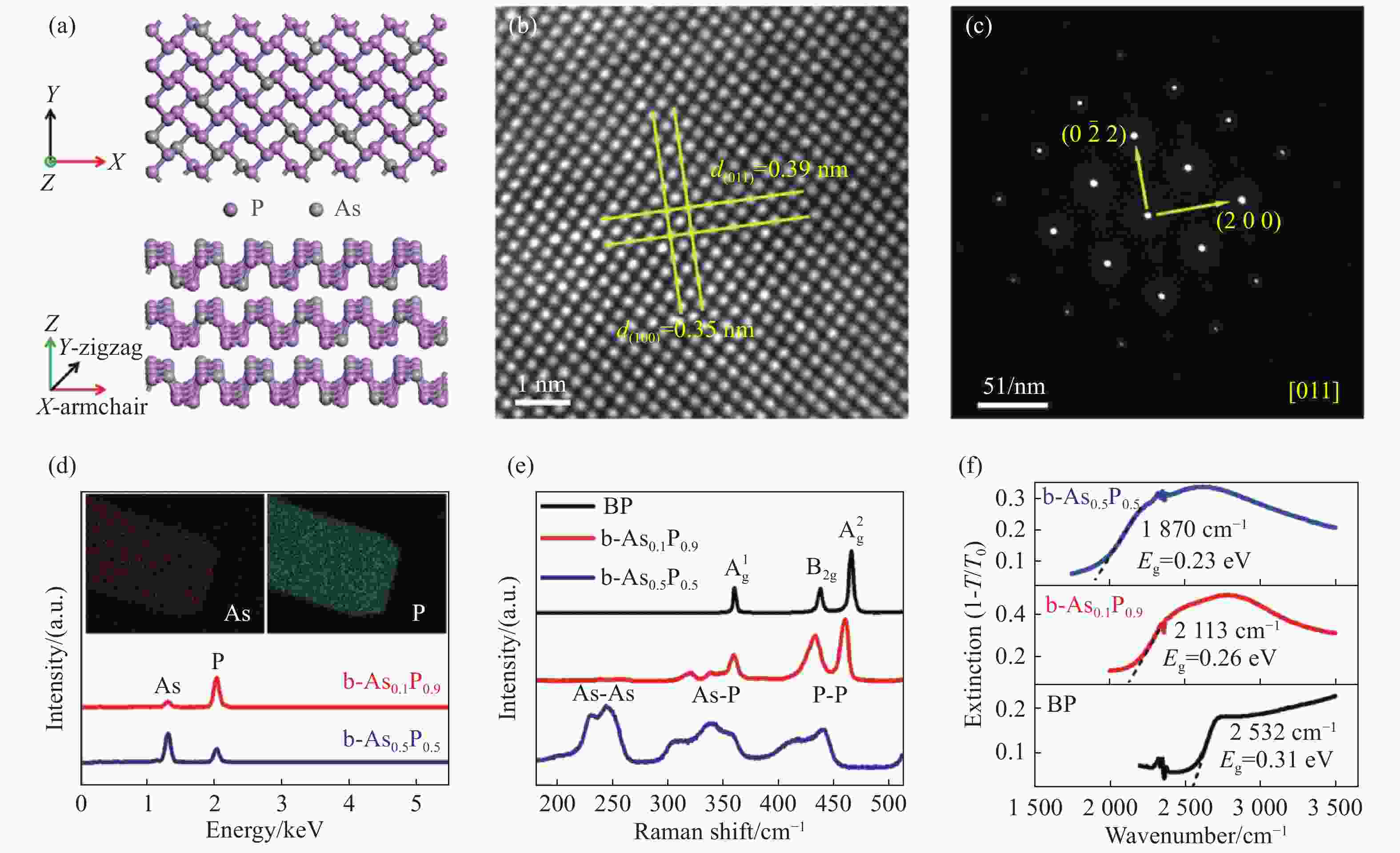
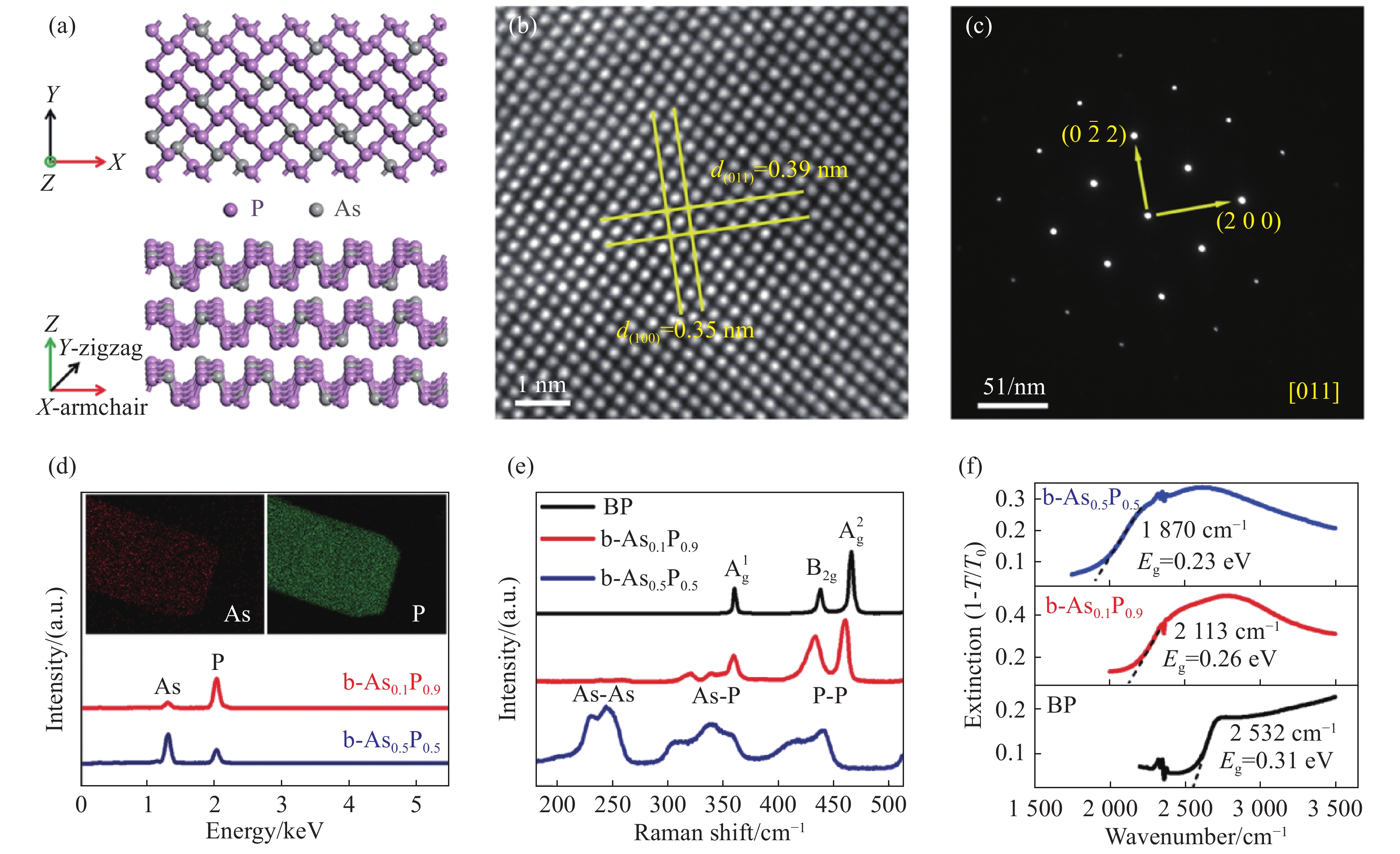
Figure 1. (a) Top view and side view of the b-AsxP1−x crystal structure. (The armchair (X) and zigzag (Y) crystal axis are shown on the graph) (b) The HRTEM image of the b-As0.1P0.9. (c) The corresponding SAED pattern of the b-As0.1P0.9. (d) EDX result of the b-AsxP1−x (x=0.1 and 0.5) flakes, insert: EDS elemental mapping of the b-As0.1P0.9. (e) Raman spectra of b-AsxP1−x with different chemical compositions. (f) Plots of infrared absorption of different b-AsxP1−x samples
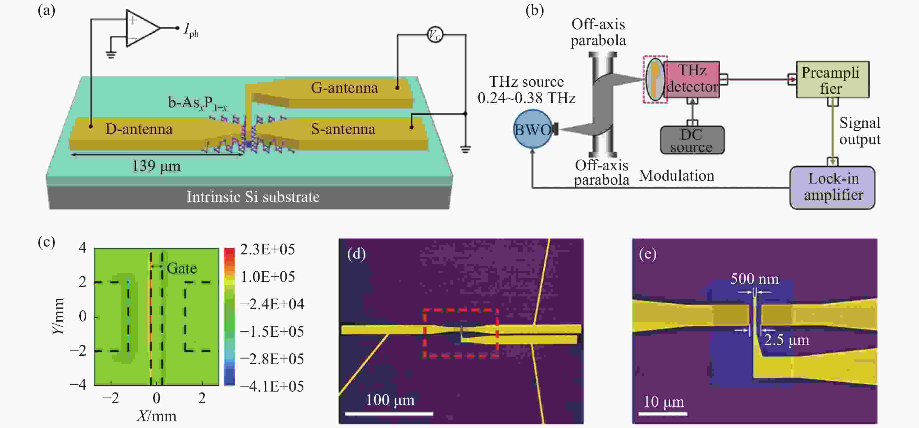
Figure 2. (a) Schematic diagram of the b-AsxP1−x detector, including the measurement circuit. (b) Schematic diagram of the measurement system. (c) Spatial distributions of the field enhancement factors for the THz antenna. (d, e) False-color SEM image of the b-AsxP1−x detector

Figure 3. (a, c) Output characteristics of the b-As0.1P0.9 detector (a) and b-As0.5P0.5 detector (c), with VG ranging from −6 V to 6 V with steps of 3 V. Transfer characteristics for the b-As0.1P0.9 detector (b) and the b-As0.5P0.5 detector (d) with a fixed VDS = 50 mV
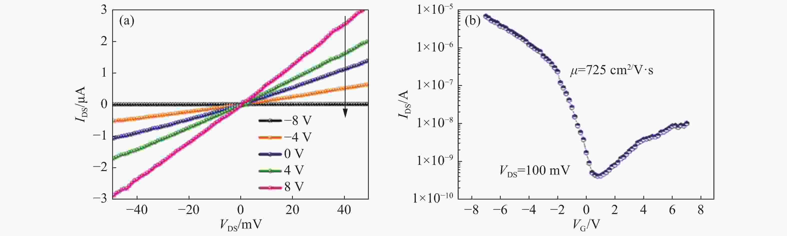
The electrical properties of the as-fabricated BP detector. (a) Output characteristics of the BP detector as function of different VG from −8 V to 8 V with steps of 4 V. It shows a good Ohmic contact and a large tunable of carrier density by gate voltage. (b) Transfer characteristics for the BP detector with a fixed VDS=100 mV. It exhibits a typical p-type ambipolar transport behavior. The field-effect hole mobility measured from the transfer curve is about 725 cm2/V·s.
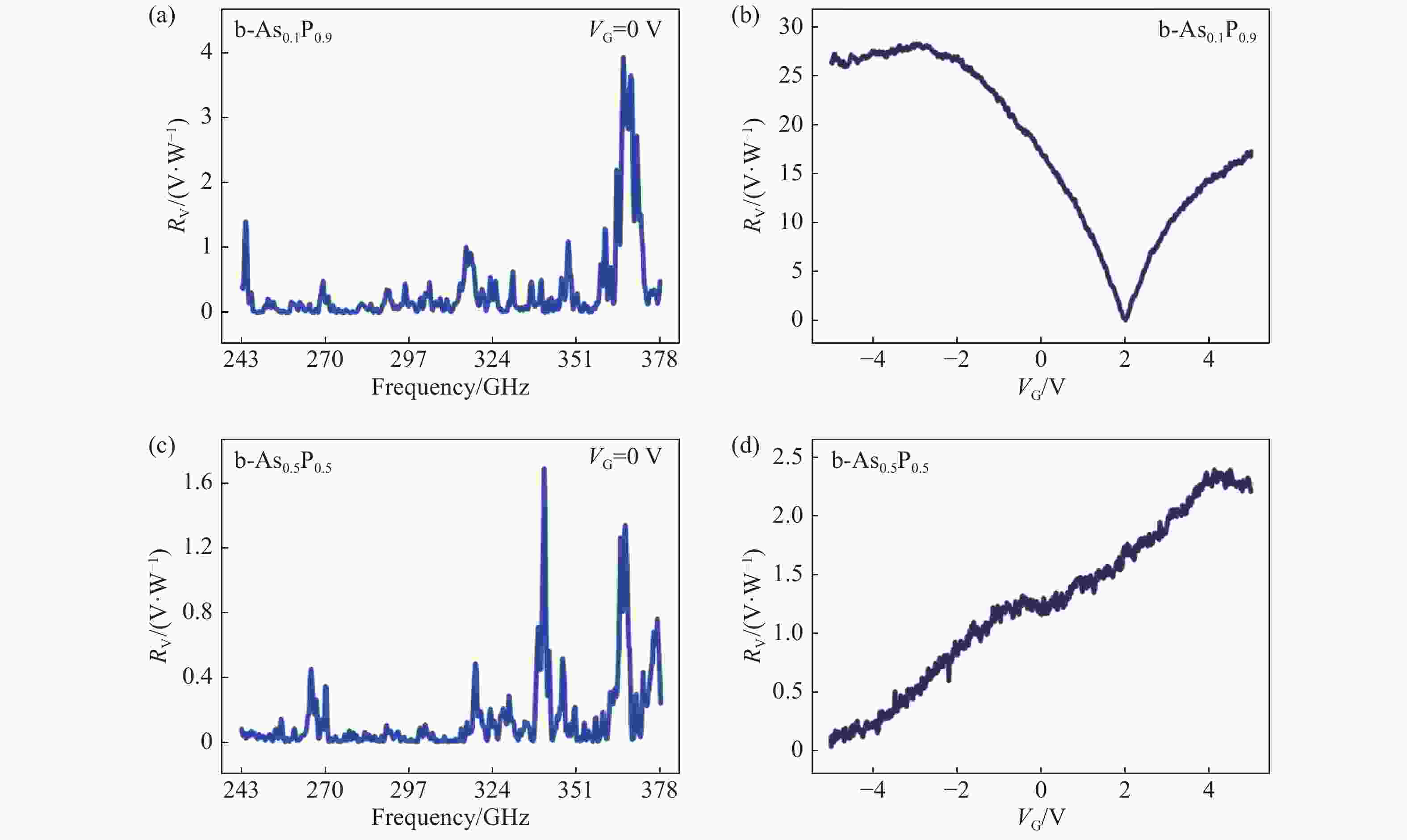
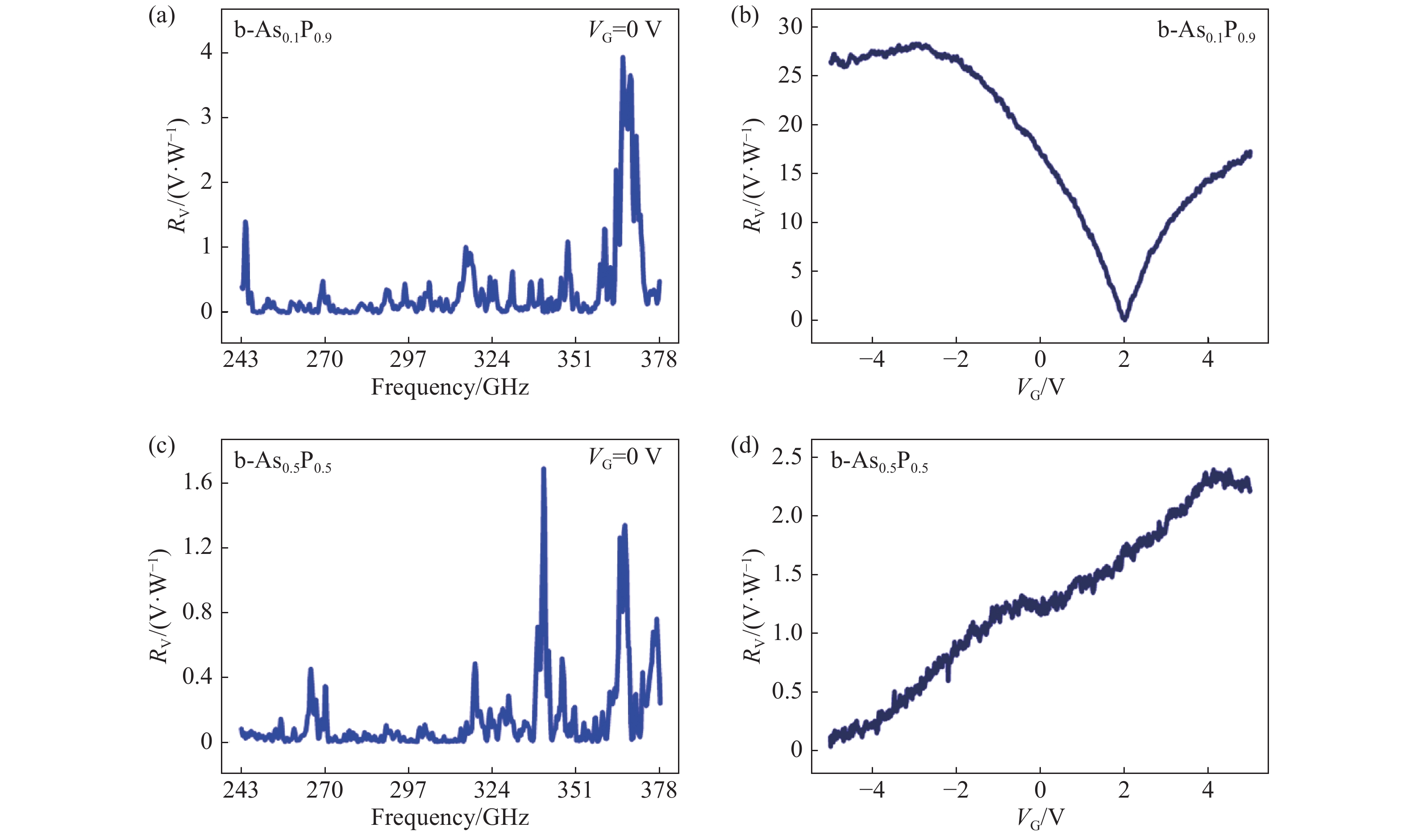
Figure 4. Frequency dependence of the responsivity for the b-As0.1P0.9 detector (a) and b-As0.5P0.5 detector (c), measured at VG = 0 V. Gate bias dependence of the responsivity for the b-As0.1P0.9 detector (b) and the b-As0.5P0.5 detector (d), measured at the optimal frequency as obtained from (a) and (c), respectively
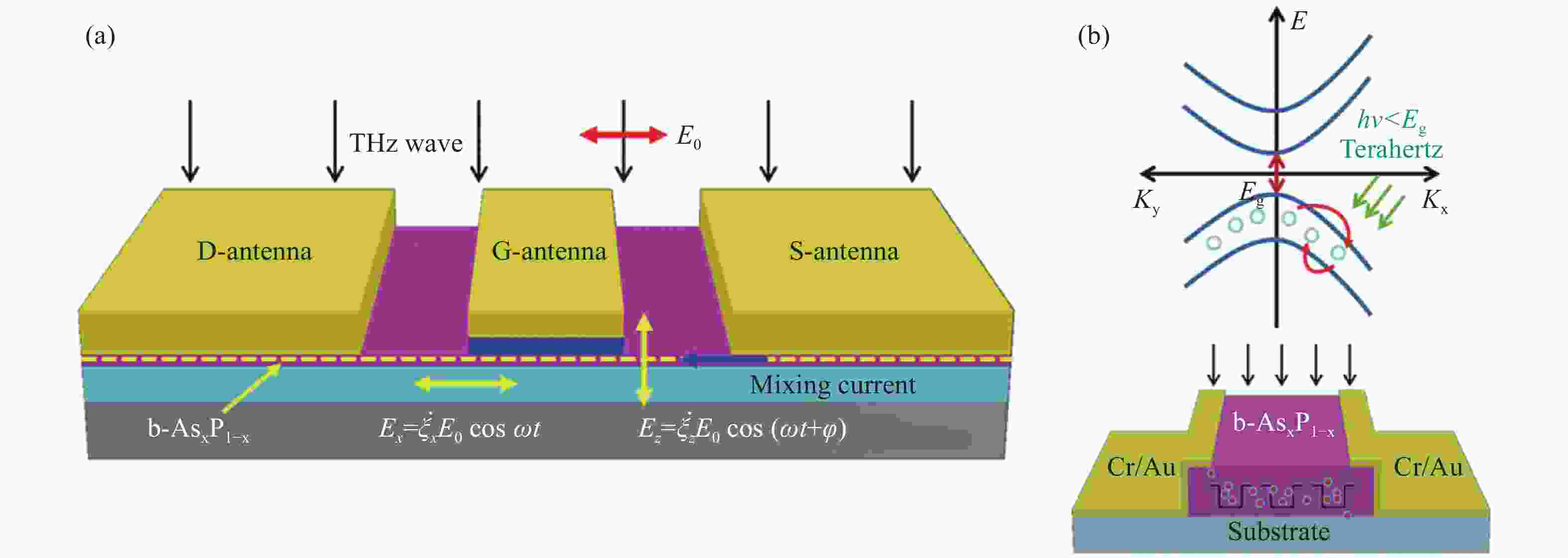
Figure 5. (a) Schema of the detector based on the self-mixing theory. (b) Photo-excitation and relaxation processes of the carriers in the b-AsxP1−x flakes irradiated by terahertz photons and the schematic diagram of the MSM structure based on EIW theory
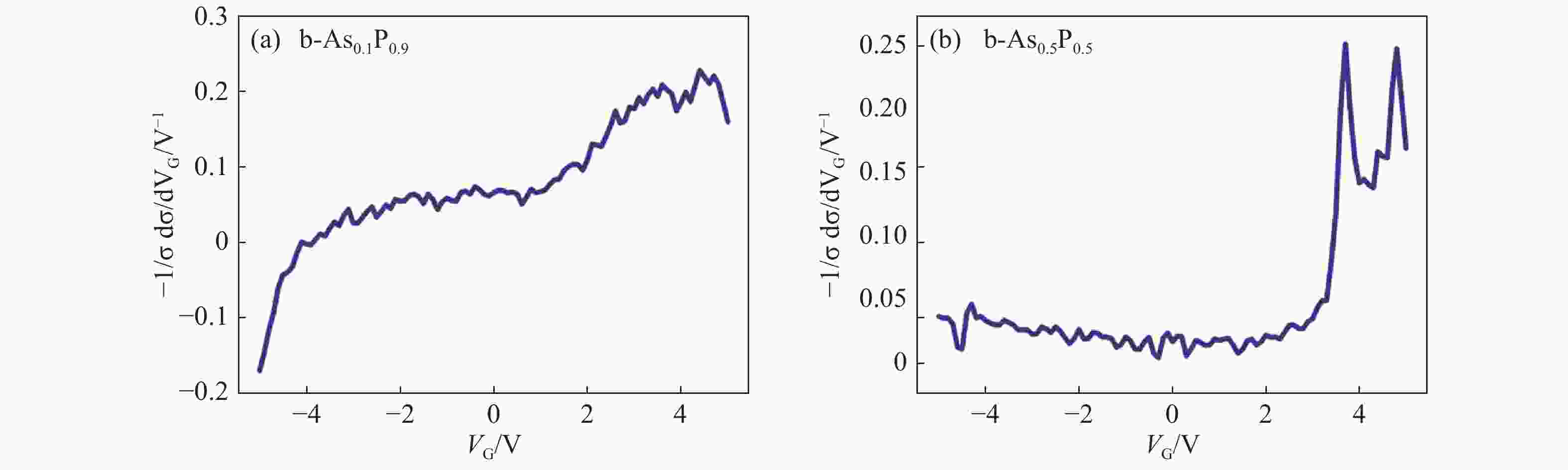
Derivative of conductivity multiplied by the resistance, as a function of VG, in b-As0.1P0.9(a) and b-As0.5P0.5 (b) detector. This is the expected responsivity following a plasma-wave detection mechanism. If the domain mechanism is the PW mechanism, the measured shape of the RV curve should be in excellent agreement with that curves.
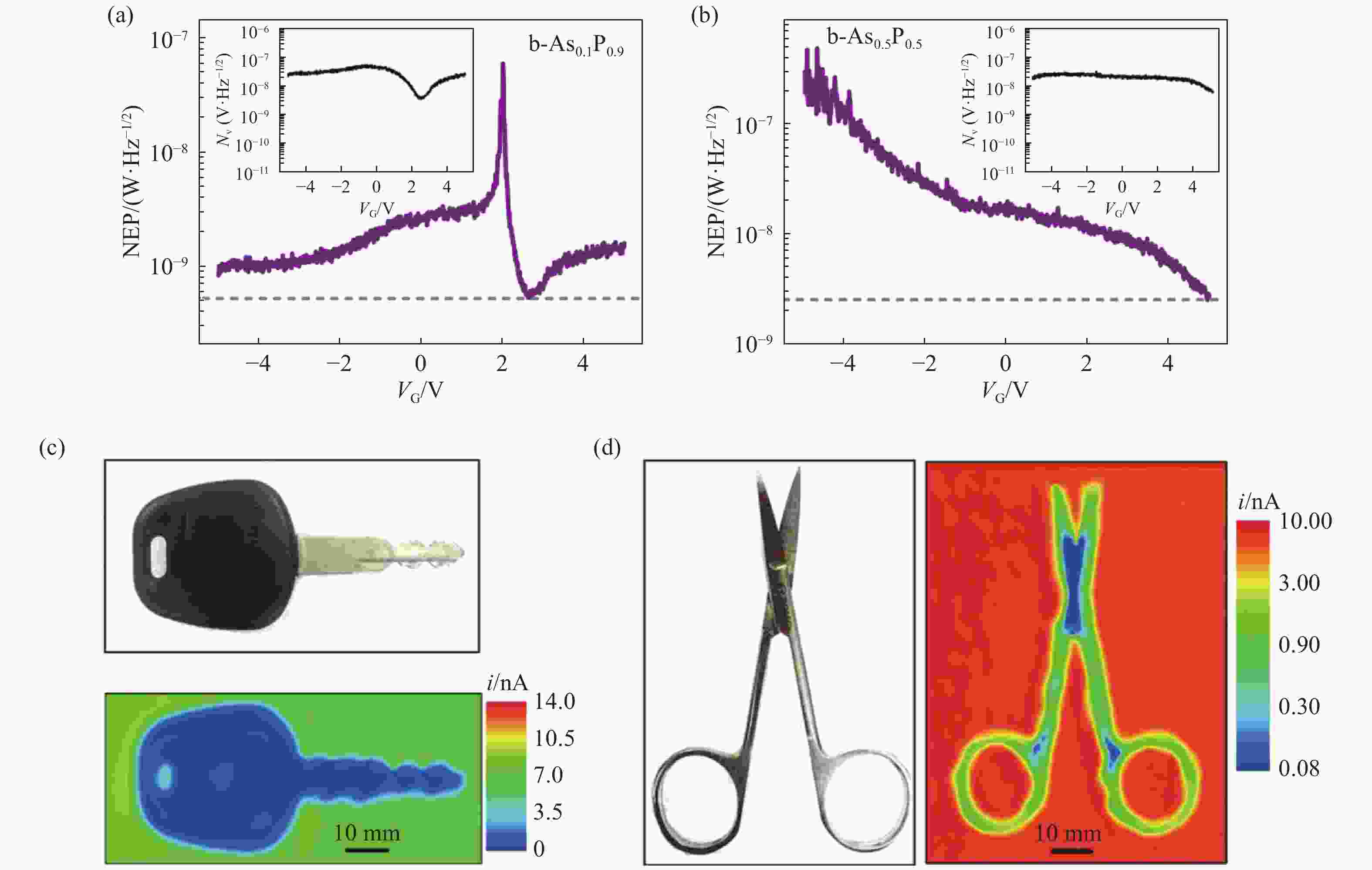
Figure 6. NEP as a function of the gate voltage for b-As0.1P0.9 detector(a) and b-As0.5P0.5 detector (b), insert: NV as a function of the VG. Transmission images of a key (c) and a pair of metal scissors (d) inside an envelope by the b-As0.1P0.9 detector at 0.37 THz
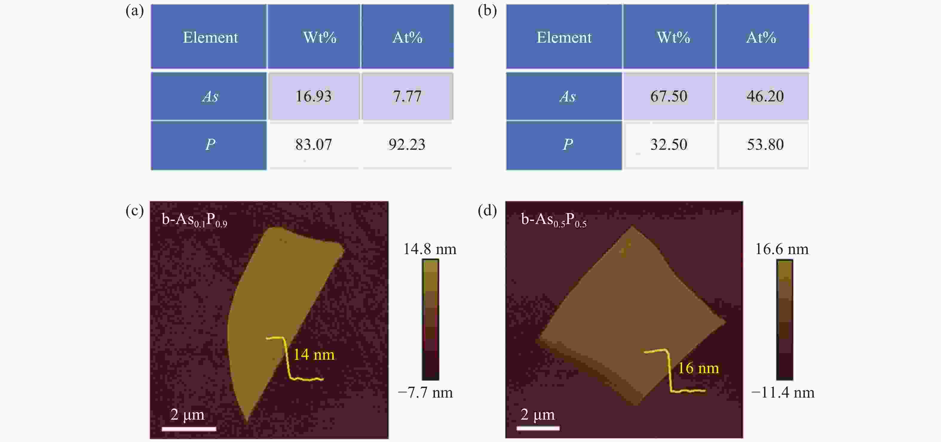
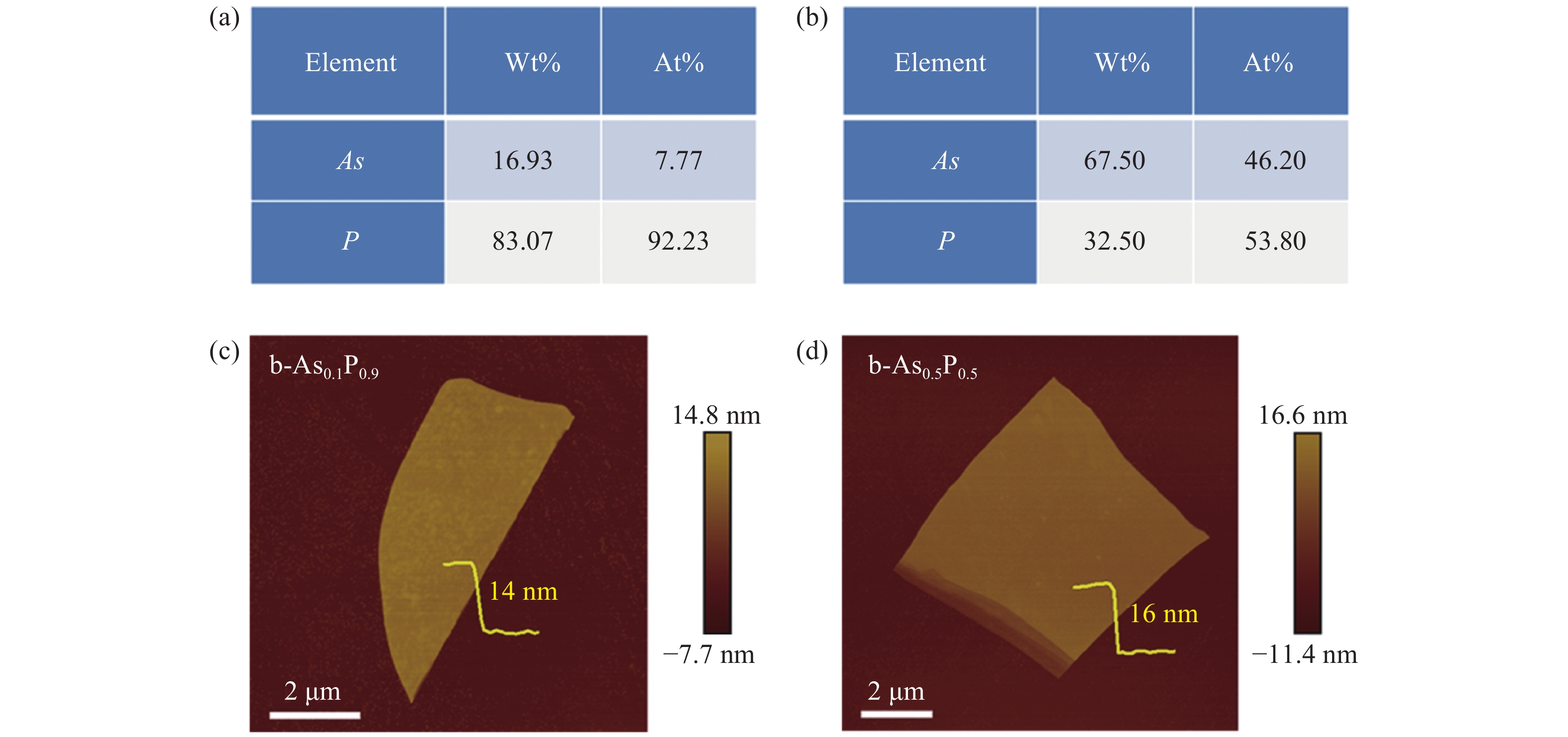
(a, b) Atomic ratio of As and P elements for the b-As0.1P0.9 and b-As0.5P0.5, respectively. It proves the b-As0.1P0.9 and b-As0.5P0.5 have an accurate elemental ratio of about 1:9 and 5:5. (c, d) The AFM images of few-layer b-As0.1P0.9 and b-As0.5P0.5 nanoflakes on a Si substrate with 285 nm SiO2. It shows clean surface and flat shape, proving the high quality of the mateials. And the corresponding linear scan analysis of height display in the images with a thickness of 14 nm and 16 nm for b-As0.1P0.9 and b-As0.5P0.5 nanoflakes, respectively.

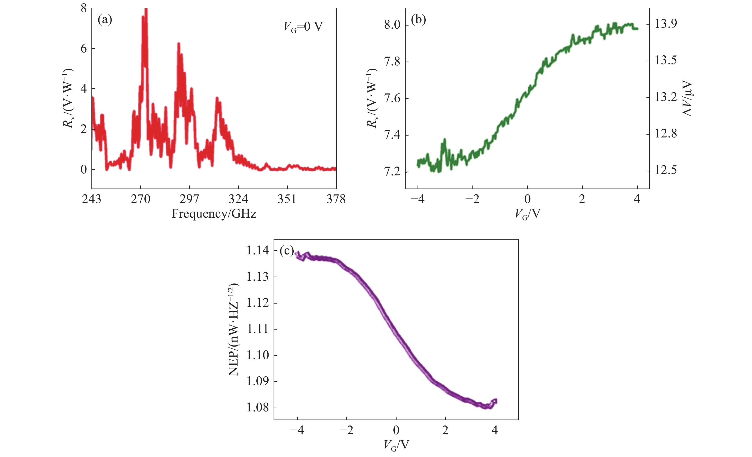
The terahertz response characteristics of the same BP detector. (a) Frequency dependence of the voltage responsivityfor BP detector at VG = 0 V. It shows several clear response peaks for the detector and the maximum voltage responsivity located at 0.27 THz.(b, c) Voltage responsivity and noise equivalent power as a function of the gate voltage at 0.27 THz. The maximum RV and minimum NEP of about 8.1 V/W and 1.08 nW/Hz1/2 were measured from the curve, respectively.
-
[1] GUO W L, WANG L, CHEN X SH, et al. Graphene-based broadband terahertz detector integrated with a square-spiral antenna[J]. Optics Letters, 2018, 43(8): 1647-1650. doi: 10.1364/OL.43.001647 [2] CASTILLA S, TERRÉS B, AUTORE M, et al. Fast and sensitive terahertz detection using an antenna-integrated graphene pn junction[J]. Nano Letters, 2019, 19(5): 2765-2773. doi: 10.1021/acs.nanolett.8b04171 [3] VITI L, PURDIE D G, LOMBARDO A, et al. HBN-encapsulated, graphene-based, room-temperature terahertz receivers, with high speed and low noise[J]. Nano Letters, 2020, 20(5): 3169-3177. doi: 10.1021/acs.nanolett.9b05207 [4] LIU CH L, WANG L, CHEN X SH, et al. Room-temperature photoconduction assisted by hot-carriers in graphene for sub-terahertz detection[J]. Carbon, 2018, 130: 233-240. doi: 10.1016/j.carbon.2018.01.020 [5] HUANG ZH M, TONG J CH, HUANG J G, et al. Room-temperature photoconductivity far below the semiconductor bandgap[J]. Advanced Materials, 2014, 26(38): 6594-6598. doi: 10.1002/adma.201402352 [6] CHEREDNICHENKO S, HAMMAR A, BEVILACQUA S, et al. A room temperature bolometer for terahertz coherent and incoherent detection[J]. IEEE Transactions on Terahertz Science and Technology, 2011, 1(2): 395-402. doi: 10.1109/TTHZ.2011.2164654 [7] SAKHNO M, GOLENKOV A, SIZOV F. Uncooled detector challenges: millimeter-wave and terahertz long channel field effect transistor and Schottky barrier diode detectors[J]. Journal of Applied Physics, 2013, 114(16): 164503. doi: 10.1063/1.4826364 [8] ROGALSKI A, SIZOV F. Terahertz detectors and focal plane arrays[J]. Opto-Electronics Review, 2011, 19(3): 346-404. [9] SUN Y F, SUN J D, ZHOU Y, et al. Room temperature GaN/AlGaN self-mixing terahertz detector enhanced by resonant antennas[J]. Applied Physics Letters, 2011, 98(25): 252103. doi: 10.1063/1.3601489 [10] VITI L, POLITANO A, VITIELLO M S. Black phosphorus nanodevices at terahertz frequencies: photodetectors and future challenges[J]. APL Materials, 2017, 5(3): 035602. doi: 10.1063/1.4979090 [11] VICARELLI L, VITIELLO M S, COQUILLAT D, et al. Graphene field-effect transistors as room-temperature terahertz detectors[J]. Nature Materials, 2012, 11(10): 865-871. doi: 10.1038/nmat3417 [12] GUO W L, DONG ZH, XU Y J, et al. Sensitive terahertz detection and imaging driven by the photothermoelectric effect in ultrashort-channel black phosphorus devices[J]. Advanced Science, 2020, 7(5): 1902699. doi: 10.1002/advs.201902699 [13] TREDICUCCI A, VITIELLO M S. Device concepts for graphene-based terahertz photonics[J]. IEEE Journal of Selected Topics in Quantum Electronics, 2014, 20(1): 8500109. [14] DYAKONOV M, SHUR M. Shallow water analogy for a ballistic field effect transistor: new mechanism of plasma wave generation by dc current[J]. Physical Review Letters, 1993, 71(15): 2465-2468. doi: 10.1103/PhysRevLett.71.2465 [15] VITI L, HU J, COQUILLAT D, et al. Efficient Terahertz detection in black-phosphorus nano-transistors with selective and controllable plasma-wave, bolometric and thermoelectric response[J]. Scientific Reports, 2016, 6: 20474. doi: 10.1038/srep20474 [16] CAI X H, SUSHKOV A B, SUESS R J, et al. Sensitive room-temperature terahertz detection via the photothermoelectric effect in graphene[J]. Nature Nanotechnology, 2014, 9(10): 814-819. doi: 10.1038/nnano.2014.182 [17] NOVOSELOV K S, GEIM A K, MOROZOV S V, et al. Electric field effect in atomically thin carbon films[J]. Science, 2004, 306(5696): 666-669. doi: 10.1126/science.1102896 [18] MANZELI S, OVCHINNIKOV D, PASQUIER D, et al. 2D transition metal dichalcogenides[J]. Nature Reviews Materials, 2017, 2(8): 17033. doi: 10.1038/natrevmats.2017.33 [19] MELLNIK A R, LEE J S, RICHARDELLA A, et al. Spin-transfer torque generated by a topological insulator[J]. Nature, 2014, 511(7510): 449-451. doi: 10.1038/nature13534 [20] LI L K, YU Y J, YE G J, et al. Black phosphorus field-effect transistors[J]. Nature Nanotechnology, 2014, 9(5): 372-377. doi: 10.1038/nnano.2014.35 [21] HU Y, QI ZH H, LU J Y, et al. van der Waals epitaxial growth and interfacial passivation of two-dimensional single-crystalline few-layer gray arsenic nanoflakes[J]. Chemistry of Materials, 2019, 31(12): 4524-4535. doi: 10.1021/acs.chemmater.9b01151 [22] QI ZH H, HU Y, JIN ZH, et al. Tuning the liquid-phase exfoliation of arsenic nanosheets by interaction with various solvents[J]. Physical Chemistry Chemical Physics, 2019, 21(23): 12087-12090. doi: 10.1039/C9CP01052A [23] WANG X X, HU Y, MO J B, et al. Arsenene: a potential therapeutic agent for acute promyelocytic leukaemia cells by acting on nuclear proteins[J]. Angewandte Chemie International Edition, 2020, 59(13): 5151-5158. doi: 10.1002/anie.201913675 [24] BANDURIN D A, SVINTSOV D, GAYDUCHENKO I, et al. Resonant terahertz detection using graphene plasmons[J]. Nature Communications, 2018, 9(1): 5392. doi: 10.1038/s41467-018-07848-w [25] LIU CH L, WANG L, CHEN X SH, et al. Top-gated black phosphorus phototransistor for sensitive broadband detection[J]. Nanoscale, 2018, 10(13): 5852-5858. doi: 10.1039/C7NR09545G [26] TANG W W, POLITANO A, GUO CH, et al. Ultrasensitive room-temperature terahertz direct detection based on a bismuth selenide topological insulator[J]. Advanced Functional Materials, 2018, 28(31): 1801786. doi: 10.1002/adfm.201801786 [27] QIN H, SUN J D, LIANG SH X, et al. Room-temperature, low-impedance and high-sensitivity terahertz direct detector based on bilayer graphene field-effect transistor[J]. Carbon, 2017, 116: 760-765. doi: 10.1016/j.carbon.2017.02.037 [28] VITI L, COQUILLAT D, POLITANO A, et al. Plasma-wave terahertz detection mediated by topological insulators surface states[J]. Nano Letters, 2016, 16(1): 80-87. doi: 10.1021/acs.nanolett.5b02901 [29] XIE Y, LIANG F, CHI SH M, et al. Defect engineering of MoS2 for room-temperature terahertz photodetection[J]. ACS Applied Materials &Interfaces, 2020, 12(6): 7351-7357. [30] LIU B L, KÖPF M, ABBAS A N, et al. Black arsenic-phosphorus: layered anisotropic infrared semiconductors with highly tunable compositions and properties[J]. Advanced Materials, 2015, 27(30): 4423-4429. doi: 10.1002/adma.201501758 [31] PRADHAN N R, GARCIA C, LUCKING M C, et al. Raman and electrical transport properties of few-layered arsenic-doped black phosphorus[J]. Nanoscale, 2019, 11(39): 18449-18463. doi: 10.1039/C9NR04598H [32] LONG M SH, GAO A Y, WANG P, et al. Room temperature high-detectivity mid-infrared photodetectors based on black arsenic phosphorus[J]. Science Advances, 2017, 3(6): e1700589. doi: 10.1126/sciadv.1700589 [33] TAN W C, HUANG L, NG R J, et al. A black phosphorus carbide infrared phototransistor[J]. Advanced Materials, 2018, 30(6): 1705039. doi: 10.1002/adma.201705039 [34] WU F, XIA H, SUN H D, et al. AsP/InSe van der waals tunneling heterojunctions with ultrahigh reverse rectification ratio and high photosensitivity[J]. Advanced Functional Materials, 2019, 29(12): 1900314. doi: 10.1002/adfm.201900314 [35] SHI X Y, WANG T, WANG J, et al. Synthesis of black arsenic-phosphorus and its application for Er-doped fiber ultrashort laser generation[J]. Optical Materials Express, 2019, 9(5): 2348-2357. doi: 10.1364/OME.9.002348 [36] SUN J D, QIN H, LEWIS R A, et al. Probing and modelling the localized self-mixing in a GaN/AlGaN field-effect terahertz detector[J]. Applied Physics Letters, 2012, 100(17): 173513. doi: 10.1063/1.4705306 [37] WU C Y, ZHOU W, YAO N J, et al. Silicon-based high sensitivity of room-temperature microwave and sub-terahertz detector[J]. Applied Physics Express, 2019, 12(5): 052013. doi: 10.7567/1882-0786/ab14fc [38] LI S S. Semiconductor Physical Electronics[M]. Boston, MA: Springer, 1993. [39] SUN J D, FENG W, DING Q F, et al. Smaller antenna-gate gap for higher sensitivity of GaN/AlGaN HEMT terahertz detectors[J]. Applied Physics Letters, 2020, 116(16): 161109. doi: 10.1063/1.5142436 -

 下载:
下载:


计量
- 文章访问数: 3037
- HTML全文浏览量: 1176
- PDF下载量: 222
- 被引次数: 0
