-
摘要: 线偏振光的探测能力是评价偏振光电探测器件的重要指标。黑砷磷(AsP)是一种较为稳定的平面内各向异性材料,由于其面内结构各向异性,其对线偏振光较为敏感,在偏振探测领域有着重要的应用潜力。本文介绍了一种基于AsP/MoS2的高度偏振敏感光电探测器。由于AsP各向异性的光吸收、MoS2有效的载流子收集和输运能力以及范德华异质结对暗电流的抑制作用,该光电探测器实现了大于300的电流开关比,0.27 A/W的电流光响应度以及2×1010 Jones的比探测率。更重要的是,此类光电探测器在638 nm波段实现了高达3.06二向色性比的偏振特性。这些实验结果表明AsP/MoS2异质结构在偏振光电探测领域有着广阔的应用前景。Abstract: The ability to detect linearly polarized light is an important index for evaluating polarized photoelectric detectors. Black arsenic phosphorus (b-AsP) is a relatively stable anisotropic material, and is sensitive to linearly polarized light because of its anisotropy inside its planar structure. The material has important application value in polarization detection. This paper introduces a polarization-sensitive photodetector based on AsP/MoS2. Due to the anisotropic light absorption of AsP, effective carrier collection and strong carrier transport capacity of MoS2, as well as the suppression of dark current by a van der Waals heterojunction, the performance of the photodector shows relatively large on/off ratios. Moreover, the photodector has a current optical responsivity of 0.27 A/W and a detectivity of 2×10¹⁰ Jones, and more importantly, achieves a dichroic ratio of up to 3.06 at 638 nm. These experimental results show that AsP/MoS2 heterostructures have broad application prospects in the field of polarized photoelectricity detection.
-
Key words:
- photodetectors /
- black arsenic phosphorus /
- heterojunction /
- polarization characteristics
-
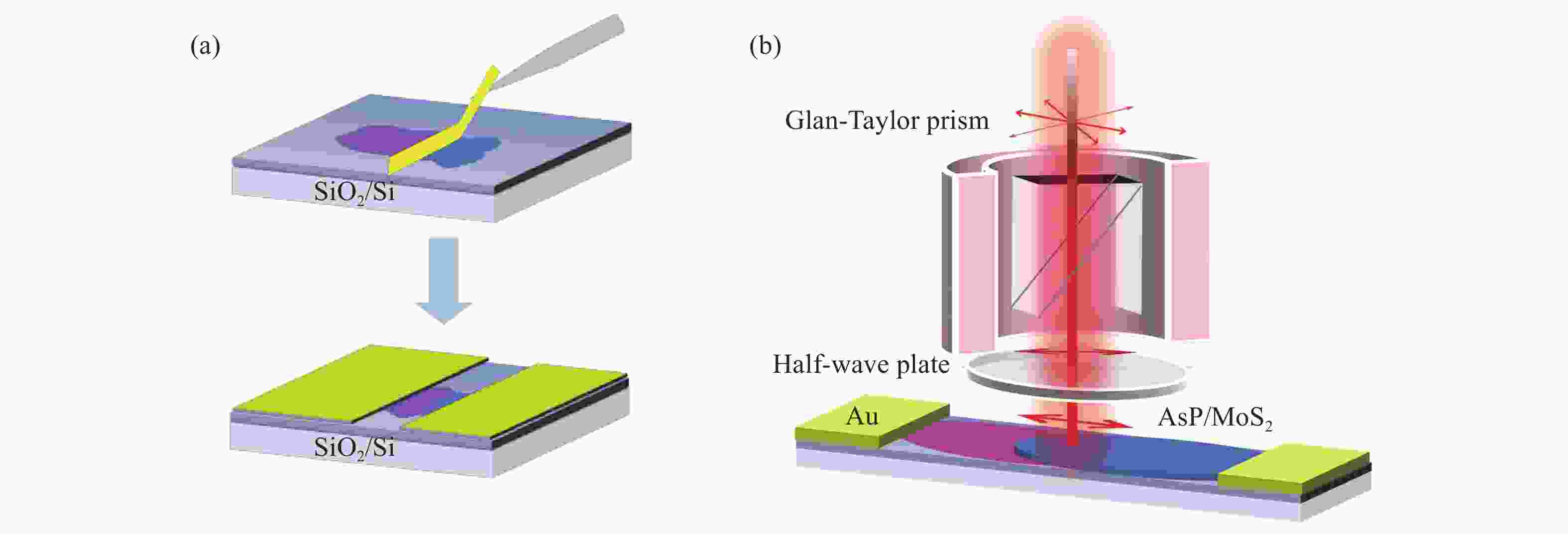
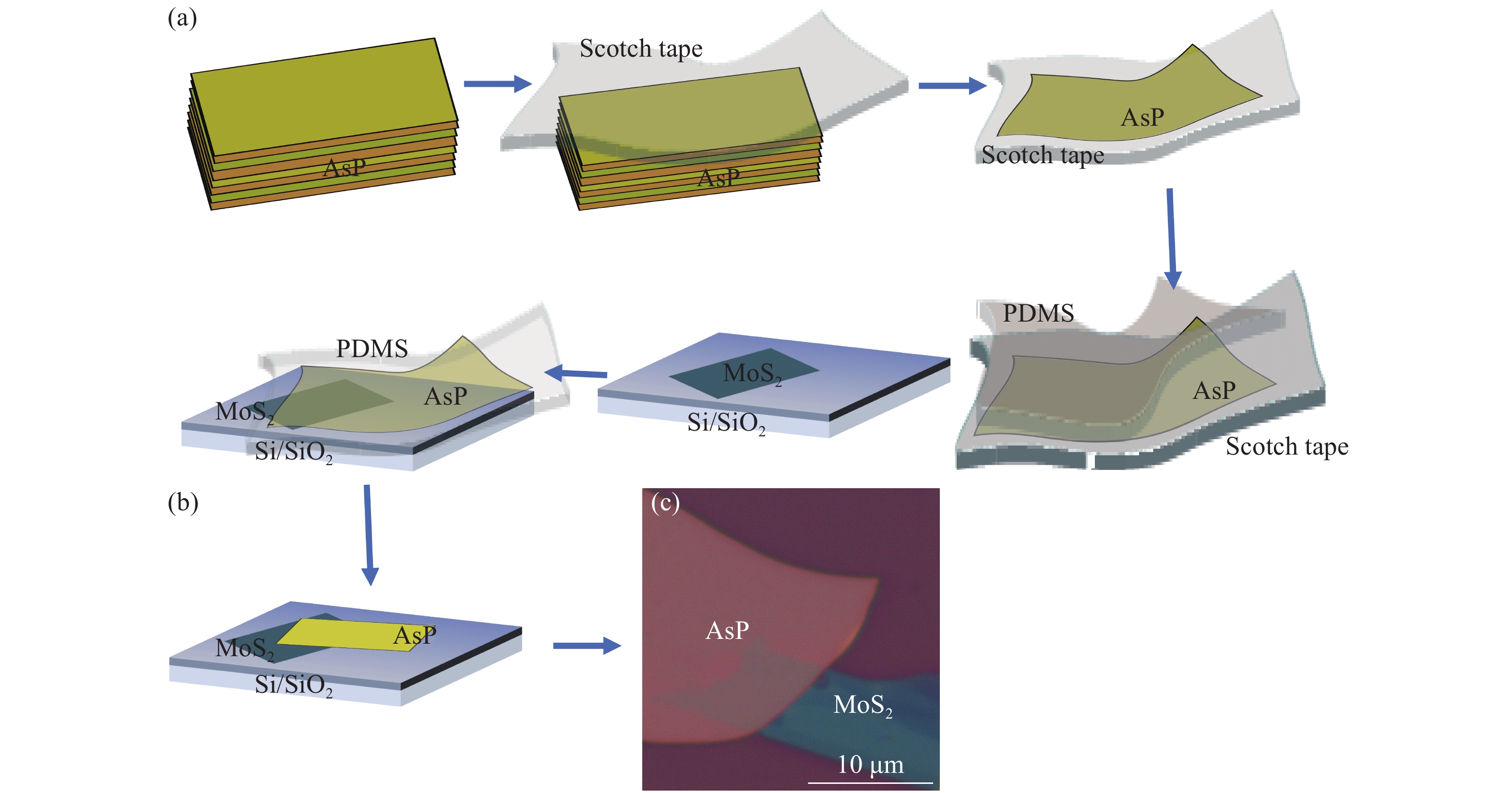
图 1 异质结制备示意图。(a)机械剥离后通过PDMS干法转移制备异质结流程图;(b)异质结构示意图;(c)异质结显微形貌图
Figure 1. Schematic diagram of heterojunction preparation. (a) Flow chart of preparing a heterojunction by PDMS dry-transfer after mechanical stripping; (b) schematic diagram of the transferred heterojunction structure; (c) microscopic morphology of the heterojunction
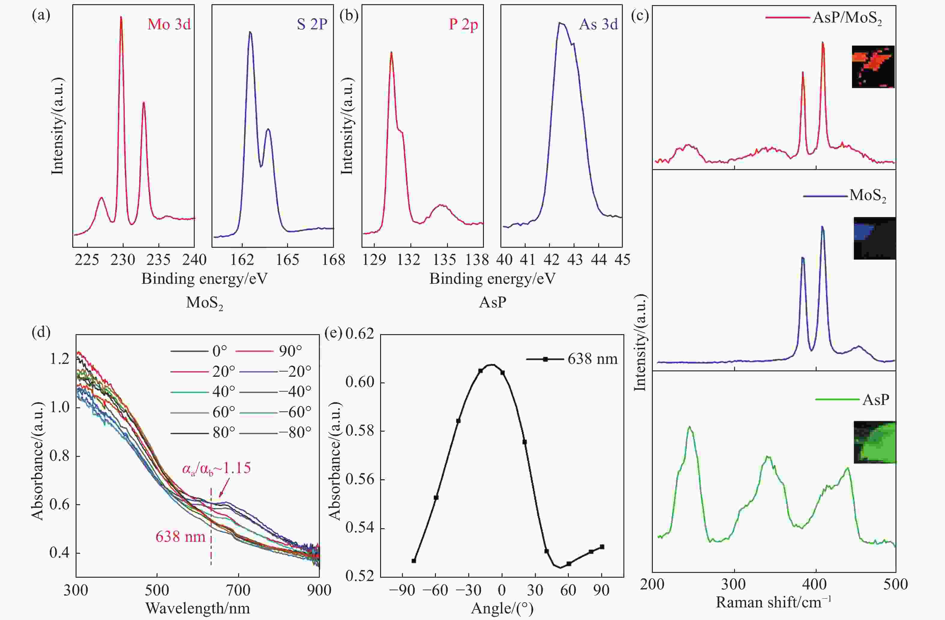
图 2 异质结表征。(a) MoS2和(b) AsP块状材料的XPS能谱;(c) 不同材料的拉曼光谱,插图为不同情况下的拉曼成像图;(d) 异质结在不同偏振光角度下的吸光度随波长变化曲线;(e) 异质结对638 nm波段的光吸收能力随入射线偏振光角度的变化曲线
Figure 2. Characterization of heterojunctions. XPS energy spectra of (a) MoS2 and (b) AsP bulk materials; (c) raman spectra of MoS2 and AsP, where the illustrations are Raman mapping diagrams under different conditions; (d) absorbance of the heterojunction varies with wavelengths under different polarized light angles; (e) absorption coefficient of the heterojunction at the 638 nm wavelength varies with the angle of linearly polarized light
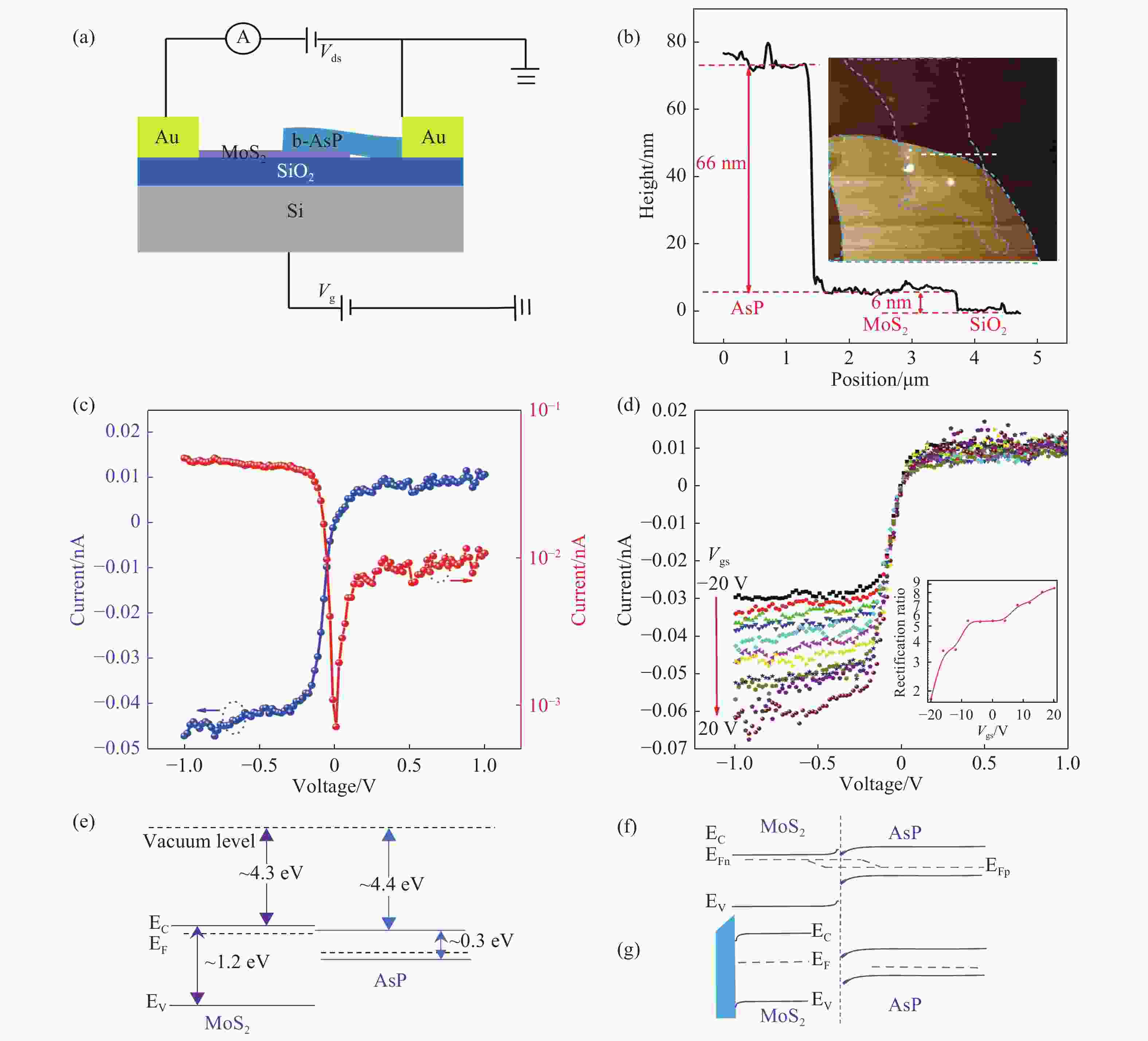
图 4 (a)测试器件示意图;(b)器件所用异质结各组分厚度,插图为异质结的原子显微图像(AFM);(c)器件伏安特性曲线(红色曲线为取对数后暗电流随电压变化情况);(d)栅压变化对伏安特性曲线的影响;(e)两种材料的能带排列(黑色水平线是真空能级);(f)正偏压下异质结的理想能带图;(g)栅压为正时,异质结正偏情况下的能带示意图
Figure 4. (a) Schematic diagram of the test device; (b) The component thickness of the heterojunction, illustrated by the Atomic Microscopic Image (AFM) of the heterojunction; (c) volt-ampere characteristics curve of the device (the red curve is the change in the dark current with voltage in a logarithmic ordinate); (d) influence of gate pressure changes on the volt-ampere characteristics curve; (e) band alignment of the two materials (the black horizontal line is the vacuum level); (f) ideal energy band diagram of the heterojunction under positive bias; (g) energy band diagram where there is positive bias in the heterojunction when the gate pressure is positive
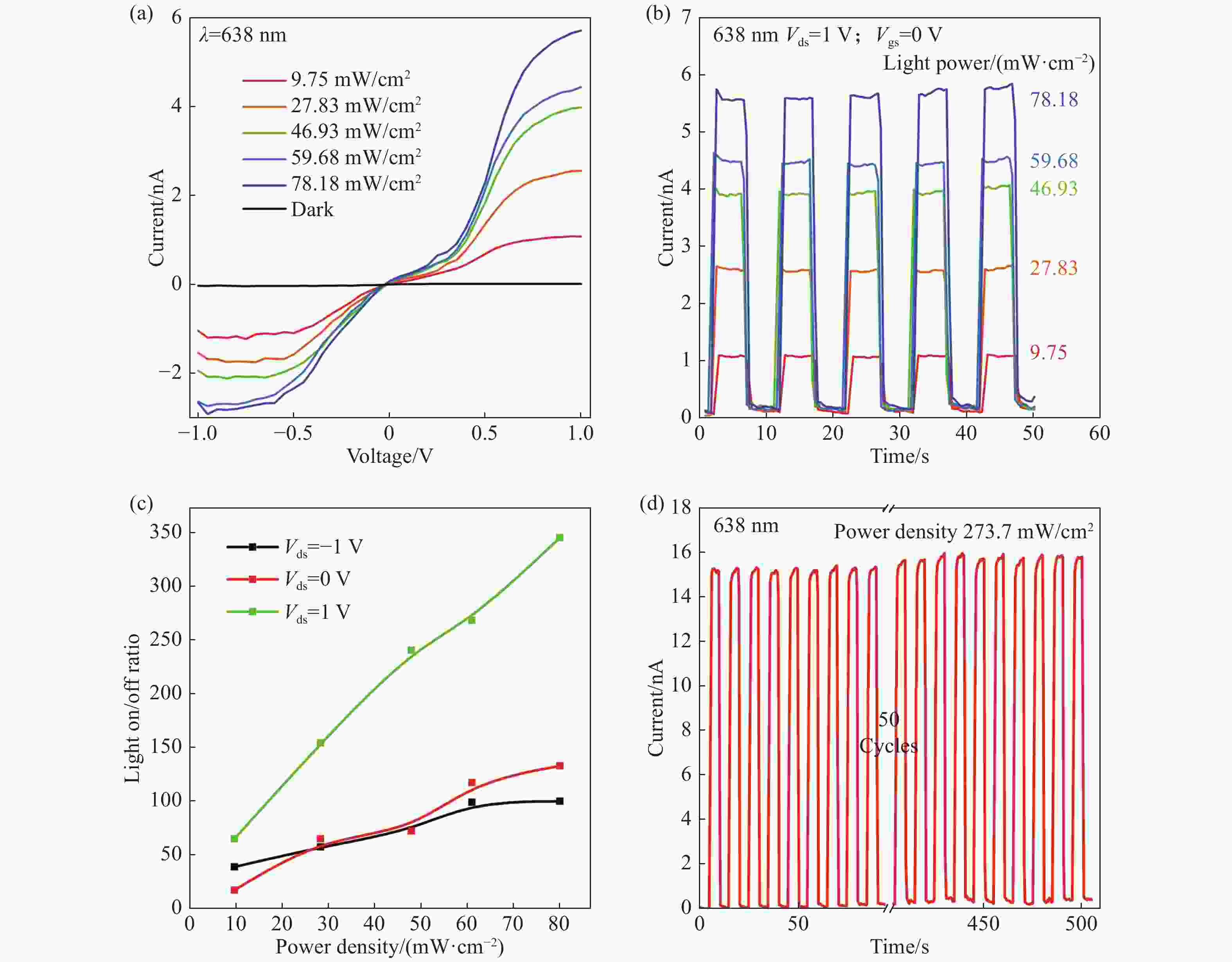
图 5 (a)不同光强下器件的伏安特性曲线;(b)不同光强下器件电流随时间变化曲线;(c)器件开关比随入射光强及源漏电压变化情况;(d)重复开关50次器件电流随时间的变化情况(Vds = 1 V, Vgs = 0 V)。
Figure 5. (a) The volt-ampere characteristics curve of the device under different power densities; (b) current of the device varies with time under different power densities; (c) switching ratio as it varies with the power density of the incident light and the source-drain voltage; (d) variation of the device current over time when the switch is repeated 50 times (Vds = 1 V, Vgs = 0 V).
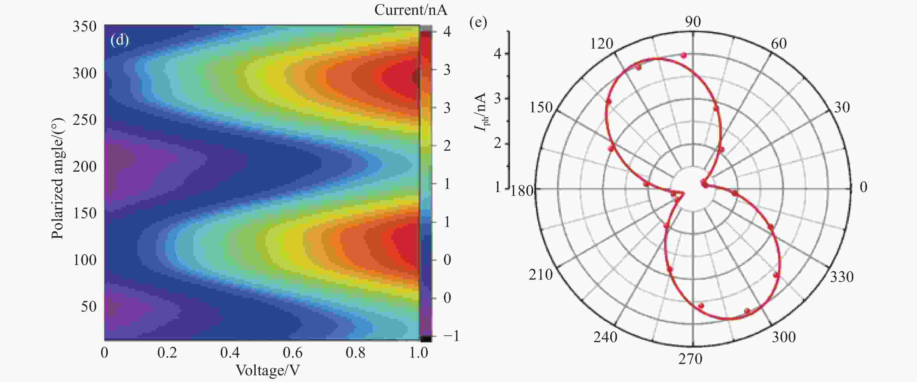
图 7 (a)偏光显微镜下水平夹角变化对材料颜色明暗的影响;(b)偏振测试时材料不同轴向的相对位置;(c)器件输出电流随入射偏振光与水平夹角变化;(d)偏振电流的各向异性响应随电压变化;(e)不同线偏振光下角分辨光电流随角度变化
Figure 7. (a) Influence of changes in the angle of polarization of the incident light on the shade of material color under a polarized light microscope; (b) axial directions of AsP during the polarization test;(c) variation curve of the current with the incident angle of polarized light; (d) anisotropic response of the polarized photocurrent varies with voltage; (e) photocurrent varies with the angle under different linearly polarized lights
-
[1] LOUIE D C, PHILLIPS J, TCHVIALEVA L, et al. Degree of optical polarization as a tool for detecting melanoma: proof of principle[J]. Journal of Biomedical Optics, 2018, 23(12): 125004. [2] 王新强, 孙晓兵, 张丽娟, 等. 可见/近红外土壤湿度的光谱偏振特性实验研究[J]. 红外与激光工程,2015,44(11):3288-3292. doi: 10.3969/j.issn.1007-2276.2015.11.021WANG X Q, SUN X B, ZHANG L J, et al. Experimental study on visible and near-infrared spectrum polarization characteristic of soil moisture[J]. Infrared and Laser Engineering, 2015, 44(11): 3288-3292. (in Chinese) doi: 10.3969/j.issn.1007-2276.2015.11.021 [3] BERNAL E O S, SABIN L, LUNA A, et al. The near-infrared polarization of the pre-planetary nebula Frosty Leo[J]. Monthly Notices of the Royal Astronomical Society, 2020, 495(3): 2599-2606. [4] PICCARDI A, COLACE L. Optical detection of dangerous road conditions[J]. Sensors, 2019, 19(6): 1360. [5] 罗曼, 吴峰, 张莉丽, 等. 二维材料偏振响应光电探测[J]. 南通大学学报(自然科学版),2019,18(3):1-10.LUO M, WU F, ZHANG L L, et al. Detection of polarized light using two-dimensional atomic materials[J]. Journal of Nantong University (Natural Science Edition) , 2019, 18(3): 1-10. (in Chinese) [6] TONG L, HUANG X Y, WANG P, et al. Stable mid-infrared polarization imaging based on quasi-2D tellurium at room temperature[J]. Nature Communications, 2020, 11(1): 2308. [7] ZHONG M Z, XIA Q L, PAN L F, et al. Thickness-dependent carrier transport characteristics of a New 2D elemental semiconductor: black arsenic[J]. Advanced Functional Materials, 2018, 28(43): 1802581. [8] ZHONG M Z, ZHOU K, WEI ZH M, et al. Highly anisotropic solar-blind UV photodetector based on large-size two-dimensional α-MoO3 atomic crystals[J]. 2D Materials, 2018, 5(3): 035033. [9] YAN Y, XIONG W Q, LI SH SH, et al. Direct wide bandgap 2D GeSe2 monolayer toward anisotropic UV photodetection[J]. Advanced Optical Materials, 2019, 7(19): 1900622. [10] WANG X T, LI Y T, HUANG L, et al. Short-wave near-infrared linear dichroism of two-dimensional germanium selenide[J]. Journal of the American Chemical Society, 2017, 139(42): 14976-17982. [11] WANG X T, WU K D, BLEI M, et al. Highly polarized photoelectrical response in vdW ZrS3 nanoribbons[J]. Advanced Electronic Materials, 2019, 5(7): 1900419. [12] ZHOU Z Q, LONG M SH, PAN L F, et al. Perpendicular optical reversal of the linear dichroism and polarized photodetection in 2D GeAs[J]. ACS Nano, 2018, 12(12): 12416-12423. [13] VENUTHURUMILLI P K, YE P D, XU X F. Plasmonic resonance enhanced polarization-sensitive photodetection by black phosphorus in near infrared[J]. ACS Nano, 2018, 12(5): 4861-4867. [14] ZHOU Q H, CHEN Q, TONG Y L, et al. Light-induced ambient degradation of few-layer black phosphorus: mechanism and protection[J]. Angewandte Chemie International Edition, 2016, 55(38): 11437-11441. [15] ZHANG L, WANG B, ZHOU Y H, et al. Synthesis techniques, optoelectronic properties, and broadband photodetection of thin-film black phosphorus[J]. Advanced Optical Materials, 2020, 8(15): 2000045. [16] LIU B L, KÖPF M, ABBAS A N, et al. Black arsenic–phosphorus: layered anisotropic infrared semiconductors with highly tunable compositions and properties[J]. Advanced Materials, 2015, 27(30): 4423-4429. [17] LONG M SH, GAO A Y, WANG P, et al. Room temperature high-detectivity mid-infrared photodetectors based on black arsenic phosphorus[J]. Science Advances, 2017, 3(6): 1700589. [18] WANG X SH, FENG H B, WU Y M, et al. Controlled synthesis of highly crystalline MoS2 flakes by chemical vapor deposition[J]. Journal of the American Chemical Society, 2013, 135(14): 5304-5307. [19] LI H, ZHANG Q, YAP C C R, et al. From bulk to monolayer MoS2: evolution of Raman scattering[J]. Advanced Functional Materials, 2012, 22(7): 1385-1390. [20] 马晶, 张光宇, 戎亦文, 等. 基于半波片的偏振跟踪理论分析[J]. 物理学报,2006,55(1):24-28. doi: 10.3321/j.issn:1000-3290.2006.01.006MA J, ZHANG G Y, RONG Y W, et al. Theoretical analysis of polarization tracking based on half-wave plate[J]. Acta Physica Sinica, 2006, 55(1): 24-28. (in Chinese) doi: 10.3321/j.issn:1000-3290.2006.01.006 [21] WU F, LI Q, WANG P, et al. High efficiency and fast van der Waals hetero-photodiodes with a unilateral depletion region[J]. Nature Communications, 2019, 10(1): 4663. [22] WANG Q SH, XU K, WANG ZH X, et al. van der waals epitaxial ultrathin two-dimensional nonlayered semiconductor for highly efficient flexible optoelectronic devices[J]. Nano Letters, 2015, 15(2): 1183-1189. [23] ZHAO J L, ZHU J J, CAO R, et al. Liquefaction of water on the surface of anisotropic two-dimensional atomic layered black phosphorus[J]. Nature Communications, 2019, 10(1): 4062. -


 下载:
下载:
