


-
摘要: 二维材料因其独特的结构和优异的电子和光电性能,为硅基光电子集成器件提供了新的发展机遇。近年来,面向硅基光电子混合集成的二维材料探测器已被广泛研究。本文梳理了构建光电探测器的几种二维材料基本特性及其探测机制,回顾了基于二维材料的硅光子集成光电探测器研究进展,总结了其器件结构和主要性能指标。最后,讨论了进一步提升硅光子集成二维材料光电探测器性能的策略,包括大规模二维材料集成器件的制备、器件结构与金属接触界面的优化以及新兴二维材料光电探测器的探索,以期推动二维材料在硅基光电子混合集成探测器领域的商业化应用。Abstract: Two-dimensional (2D) materials provide new development opportunities for silicon-based integrated optoelectronic devices due to their unique structure and excellent electronic and optoelectronic properties. In recent years, 2D material-based photodetectors for hybrid-integrated silicon photonics have been widely studied. Based on the basic characteristics of several 2D materials and the photodetection mechanisms, this paper reviews the research progress of silicon photonic integrated photodetectors based on 2D materials and summarizes existing device structure and performance. Finally, prospects for strategies to obtain high-performance silicon photonic integrated 2D material photodetectors and their commercial applicability are presented with considerations for large-scale 2D material integrations, device structure, and metal-semiconductor interface optimizations, as well as emerging 2D materials.
-
Key words:
- silicon photonics /
- 2D materials /
- photodetector
-
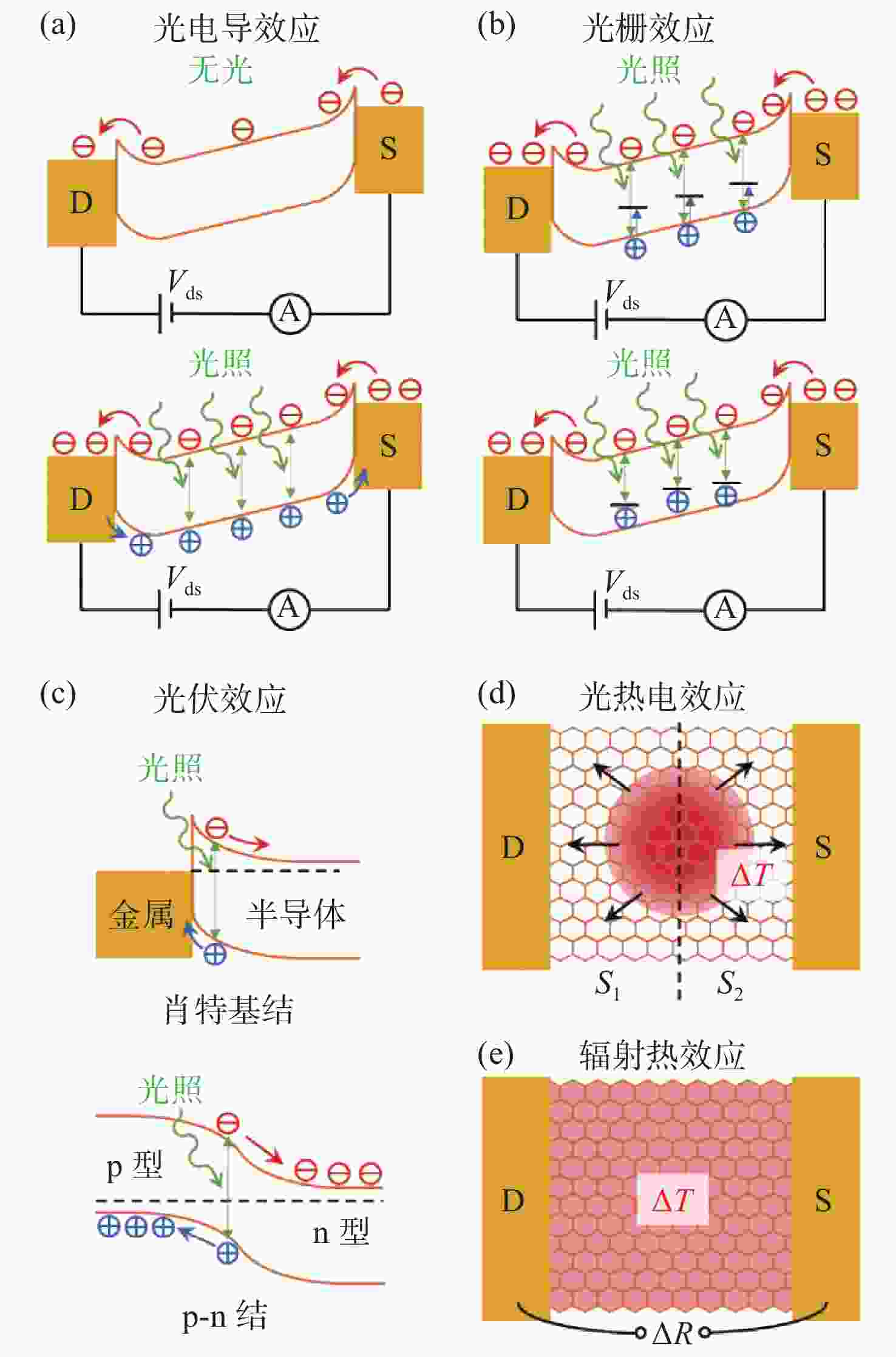
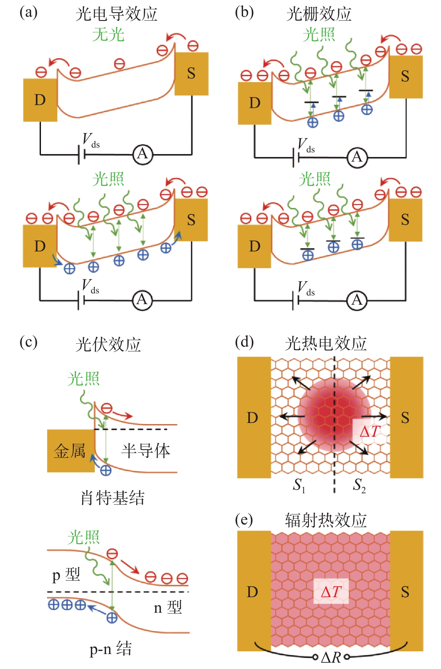
图 2 光电转换机制。(a) 光电导效应;(b) 光栅效应;(c) 光伏效应;(d) 光热电效应;(e) 辐射热效应
Figure 2. Photoelectric conversion mechanism. (a) Photoconductive effect; (b) photogating effect; (c) photovoltaic effect; (d) photo-thermoelectric effect and (e) photo-bolometric Effect
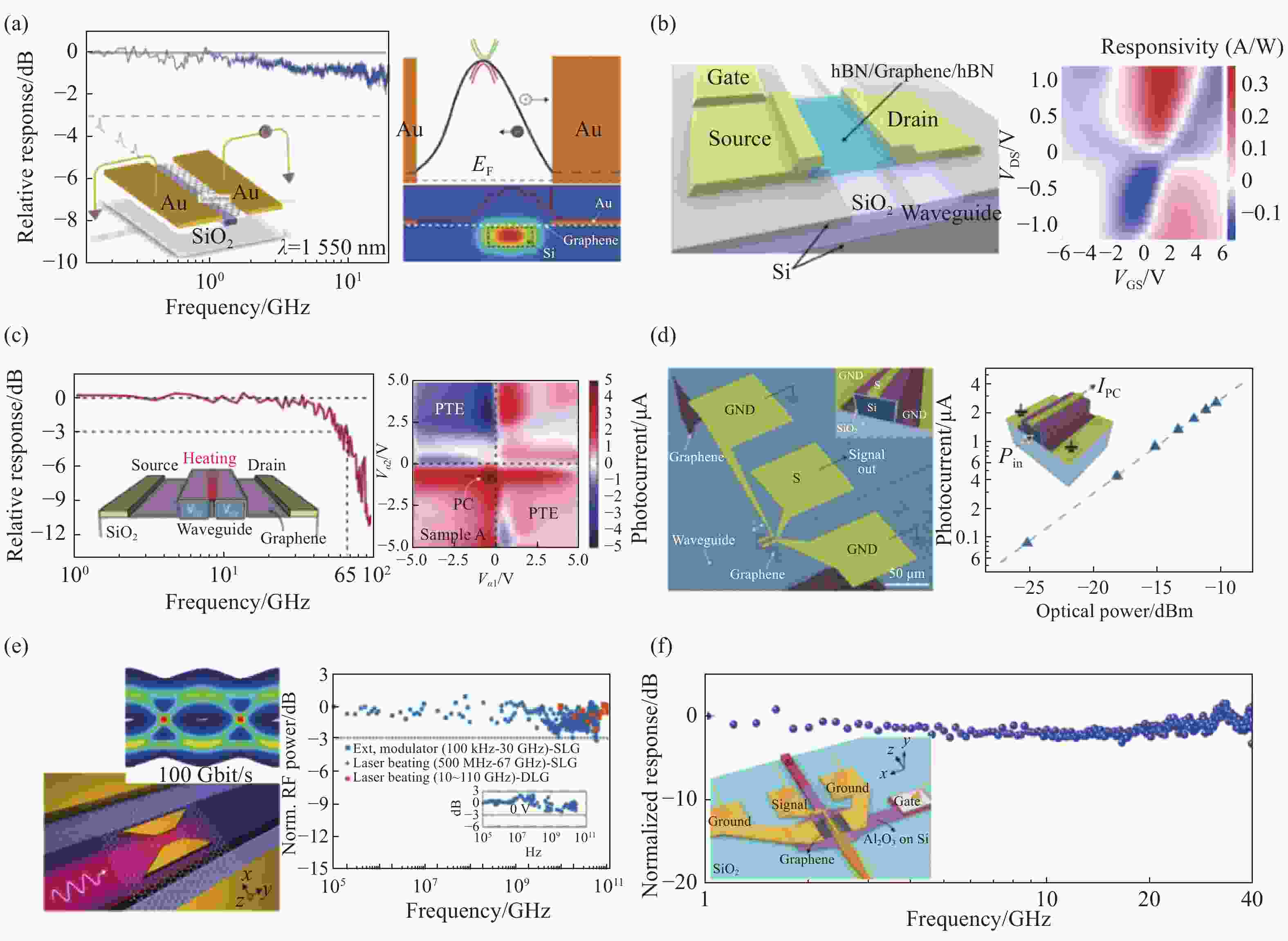
图 3 基于石墨烯的硅光子集成光电探测器。(a) 金属电极非对称的硅波导集成石墨烯光电探测器[76];(b) 硅波导集成的高响应率hBN/石墨烯/hBN结构光电探测器[79];(c) 硅纳米槽波导集成的石墨烯p-n结探测器[80];(d) 覆盖所有光通信波段且CMOS兼容的波导集成石墨烯光电探测器[78];(e) 蝴蝶结状等离子金属纳米结构增强的波导集成石墨烯光电探测器[83];(f) 用于1.55和2 μm光探测的金属等离子体增强石墨烯硅波导集成光电探测器[84]
Figure 3. Graphene-based silicon photonic integrated photodetectors. (a) A waveguide-integrated graphene photodetector with asymmetric metal electrodes[76]. (b) High-responsivity hBN/graphene/hBN photodetector on a buried silicon waveguide[79]. (c) A graphene photodetector integrated on a silicon slot-waveguide with a p-n junction[80]. (d) CMOS-compatible graphene photodetector covering all optical communication bands[78]. (e) Plasmonically-enhanced waveguide-integrated graphene photodetector. The optical field is enhanced at the edges and in the gap of the bowtie-shaped structures[83]. (f) A silicon-graphene hybrid plasmonic waveguide photodetector for 1.55 and 2 μm detection[84]
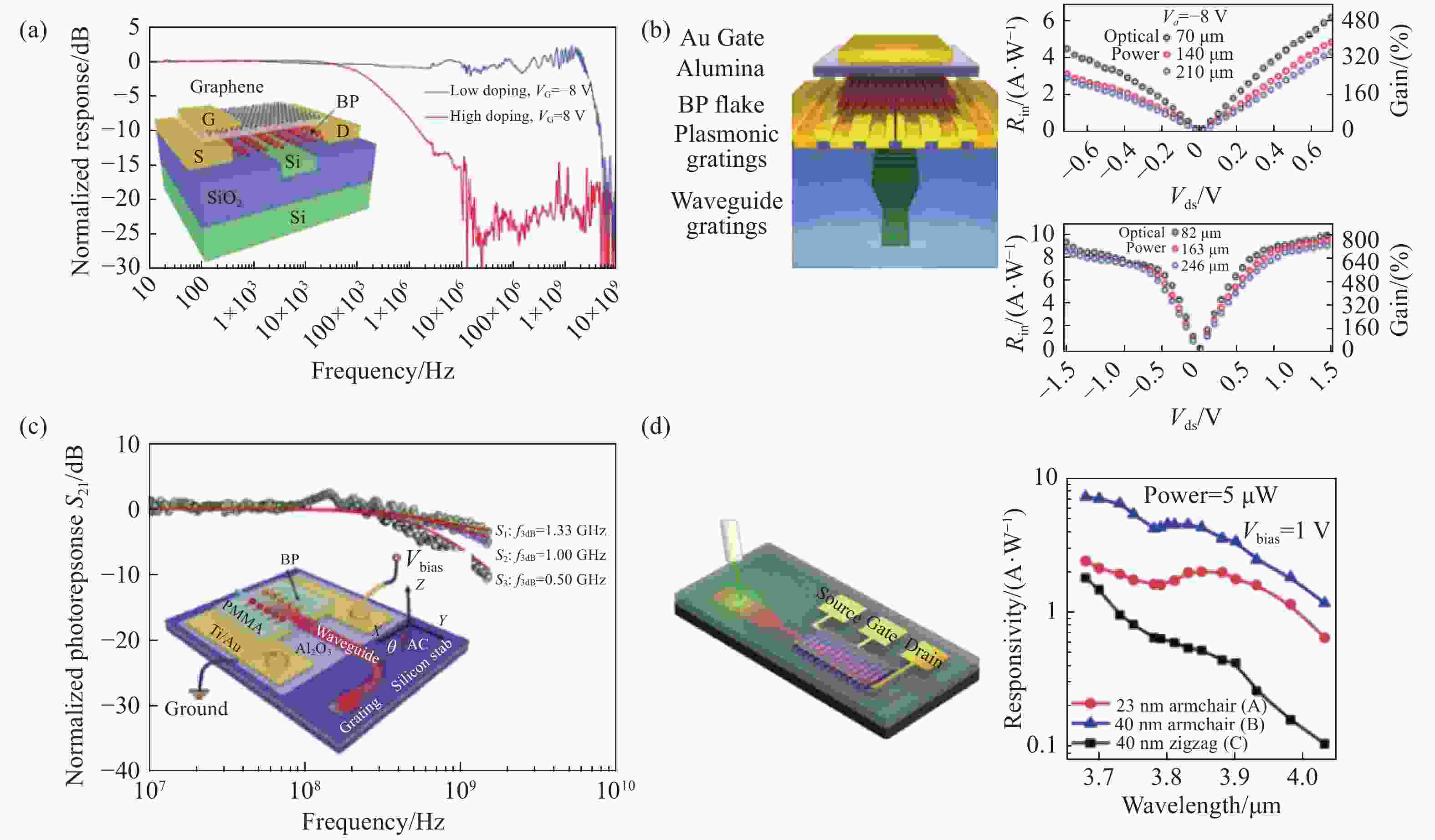
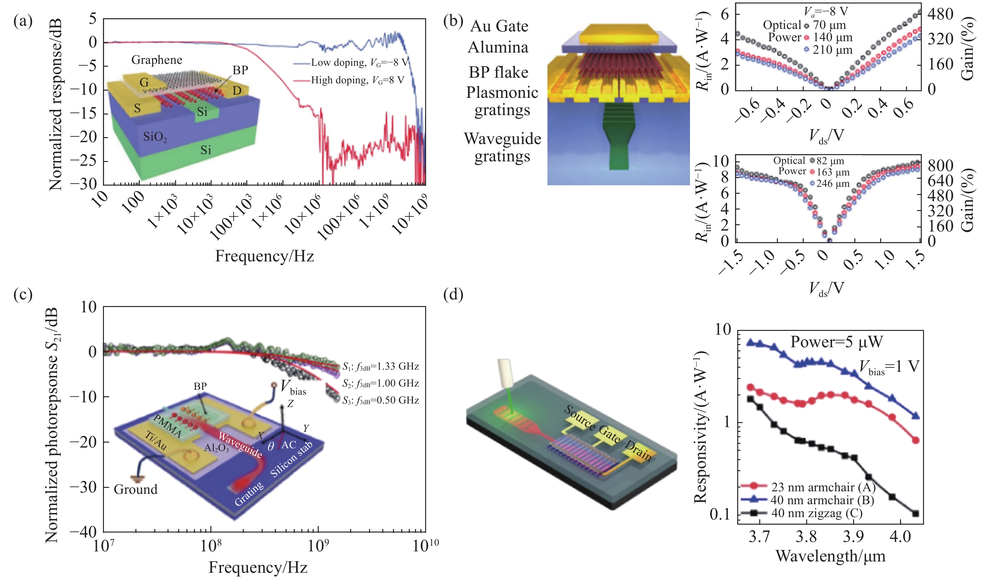
图 4 基于BP的硅光子集成光电探测器。(a) 具有高响应率和低暗电流的BP光电探测器[86];(b) 硅波导与等离子体金属光栅结构三维集成的BP光电探测器[87];(c) 工作在2 μm波长的高速高响应率硅波导集成BP光电探测器[88];(d) 可用于中红外光探测的硅波导集成BP探测器[89]
Figure 4. BP-based silicon photonic integrated photodetectors. (a) Waveguide-integrated BP photodetector with high responsivity and a low dark current[86]; (b) three-dimensional integration of a BP photodetector with silicon waveguide and nanoplasmonics grating[87]; (c) high-speed and high-responsivity hybrid silicon/BP waveguide photodetectors at 2 µm[88]; (d) waveguide-integrated BP photodetector for mid-infrared applications[89]
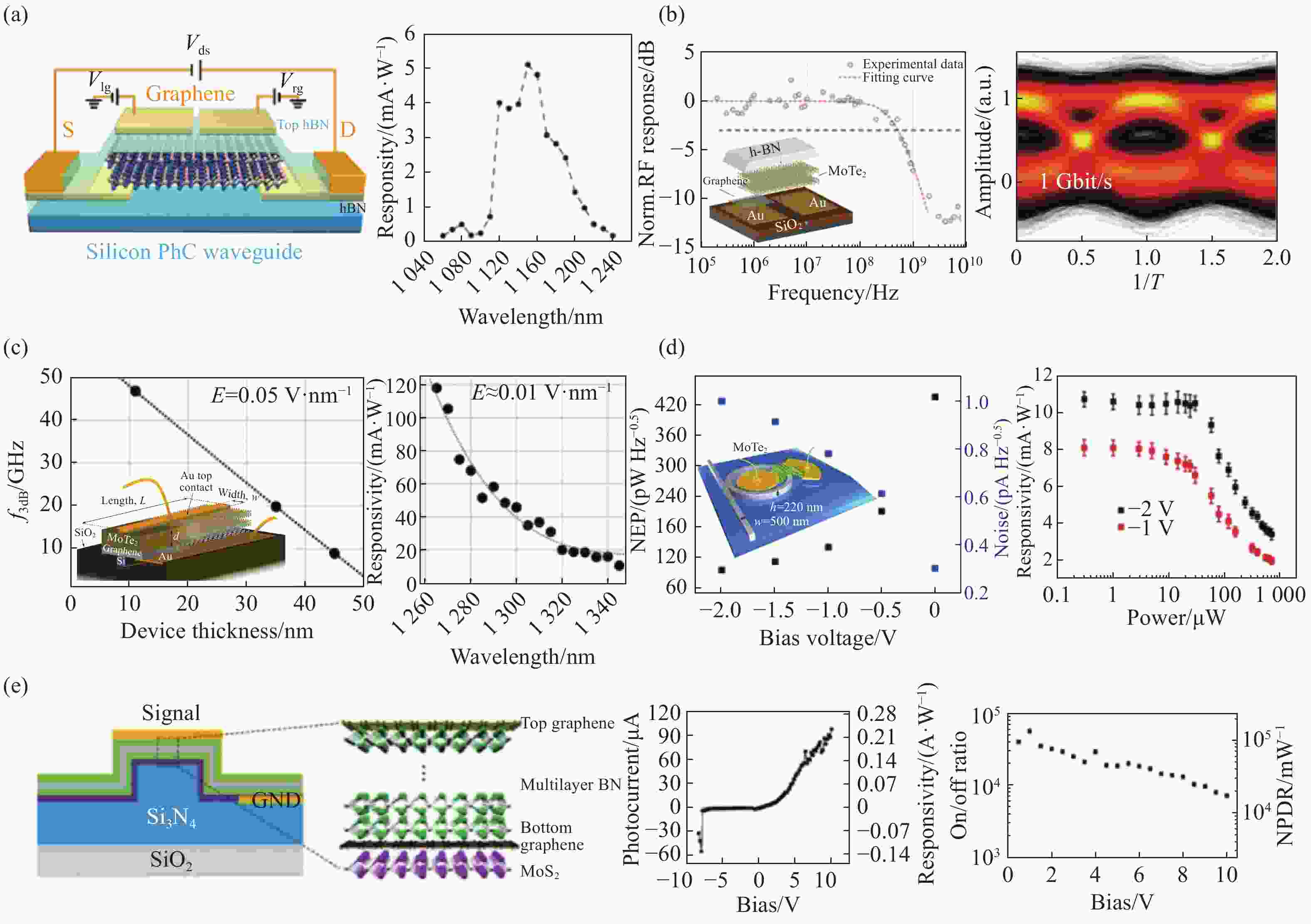
图 5 基于TMDCs及其异质结构的硅光子集成光电探测器。(a) 硅光子集成的MoTe2 p-n结光电探测器[92];(b) 基于非对称功函数接触电极的硅波导集成MoTe2探测器[93];(c) 基于MoTe2/石墨烯范德华垂直异质结的高速高响应硅波导集成光电探测器[94];(d) 基于应变调控的硅波导集成MoTe2光电探测器,可用于1550 nm光探测[95];(e) 基于范德华异质结的氮化硅波导集成隧穿光电二极管,其在1550 nm波长处具有高速高响应[96]
Figure 5. Silicon photonic integrated photodetectors based on TMDCs and their heterostructures. (a) A MoTe2-based photodetector for silicon photonic integrated circuits[92]; (b) silicon waveguide integrated MoTe2 photodetector based on asymmetric work function contact electrodes[93]; (c) waveguide-integrated van der Waals heterostructure photodetector with high speed and high responsivity[94]; (d) strain-engineered silicon photonic integrated MoTe2 photodetector for 1550 nm light detection[95]; (e) high-speed van der Waals heterostructure tunneling photodiodes integrated on silicon nitride waveguides for 1550 nm light detection[96]
-
[1] URINO Y, NAKAMURA T, ARAKAWA Y. Silicon optical interposers for high-density optical interconnects[M]. PAVESI L, LOCKWOOD D J. Silicon Photonics III: Systems and Applications. Berlin, Heidelberg: Springer, 2016: 1-39. [2] BERGMAN K, SHALF J, HAUSKEN T. Optical interconnects and extreme computing[J]. Optics and Photonics News, 2016, 27(4): 32-39. doi: 10.1364/OPN.27.4.000032 [3] HO R, MAI K W, HOROWITZ M A. The future of wires[J]. Proceedings of the IEEE, 2001, 89(4): 490-504. doi: 10.1109/5.920580 [4] FEY D. Architectures and technologies for an optoelectronic VLSI[J]. Optik, 2001, 112(7): 274-282. doi: 10.1078/0030-4026-00057 [5] 郝然. 对硅基光电子技术发展的思考[J]. 中兴通讯技术,2017,23(5):52-55.HAO R. Development of the silicon photonic technology[J]. ZTE Technology Journal, 2017, 23(5): 52-55. (in Chinese) [6] LEE K K, LIM D R, LUAN H C, et al. Effect of Size and Roughness on Light Transmission in a Si/SiO2 waveguide: experiments and model[J]. Applied Physics Letters, 2000, 77(11): 1617-1619. doi: 10.1063/1.1308532 [7] LEE B G, CHEN X G, BIBERMAN A, et al. Ultrahigh-bandwidth silicon photonic nanowire waveguides for on-chip networks[J]. IEEE Photonics Technology Letters, 2008, 20(6): 398-400. doi: 10.1109/LPT.2008.916912 [8] OSGOOD JR R M, PANOIU N C, DADAP J I, et al. Engineering nonlinearities in nanoscale optical systems: physics and applications in dispersion-engineered silicon nanophotonic wires[J]. Advances in Optics and Photonics, 2009, 1(1): 162-235. doi: 10.1364/AOP.1.000162 [9] ORCUTT J S, KHILO A, HOLZWARTH C W, et al. Nanophotonic Integration in State-of-the-Art CMOS Foundries[J]. Optics Express, 2011, 19(3): 2335-2346. doi: 10.1364/OE.19.002335 [10] YOU J, LAVDAS S, PANOIU N C. Theoretical comparative analysis of BER in multi-channel systems with strip and photonic crystal silicon waveguides[J]. IEEE Journal of Selected Topics in Quantum Electronics, 2016, 22(2): 4400810. [11] YOUNGBLOOD N, LI M. Integration of 2D materials on a silicon photonics platform for optoelectronics applications[J]. Nanophotonics, 2016, 6(6): 1205-1218. doi: 10.1515/nanoph-2016-0155 [12] BOLKHOVITYANOV Y B, PCHELYAKOV O P. GaAs epitaxy on Si substrates: modern status of research and engineering[J]. Physics-Uspekhi, 2008, 51(5): 437-456. doi: 10.1070/PU2008v051n05ABEH006529 [13] MICHEL J, LIU J F, KIMERLING L C. High-performance Ge-on-Si photodetectors[J]. Nature Photonics, 2010, 4(8): 527-534. doi: 10.1038/nphoton.2010.157 [14] AKINWANDE D, HUYGHEBAERT C, WANG C H, et al. Graphene and two-dimensional materials for silicon technology[J]. Nature, 2019, 573(7775): 507-518. doi: 10.1038/s41586-019-1573-9 [15] LIU M, YIN X B, ULIN-AVILA E, et al. A graphene-based broadband optical modulator[J]. Nature, 2011, 474(7349): 64-67. doi: 10.1038/nature10067 [16] GAO A Y, LAI J W, WANG Y J, et al. Observation of ballistic avalanche phenomena in nanoscale vertical InSe/BP heterostructures[J]. Nature Nanotechnology, 2019, 14(3): 217-222. doi: 10.1038/s41565-018-0348-z [17] LONG M SH, WANG P, FANG H H, et al. Progress, challenges, and opportunities for 2D material based photodetectors[J]. Advanced Functional Materials, 2019, 29(19): 1803807. doi: 10.1002/adfm.201803807 [18] 肖建花, 蒋亚东, 王洋, 等. 二极管型近红外聚合物光电探测器研究进展[J]. 红外技术,2020,42(10):917-926. doi: 10.3724/SP.J.7103116028XIAO J H, JIANG Y D, WANG Y, et al. Review of near-infrared polymer photodiodes[J]. Infrared Technology, 2020, 42(10): 917-926. (in Chinese) doi: 10.3724/SP.J.7103116028 [19] 朱晓秀, 葛咏, 李建军, 等. 量子点增强硅基探测成像器件的研究进展[J]. 中国光学,2020,13(1):62-74. doi: 10.3788/co.20201301.0062ZHU X X, GE Y, LI J J, et al. Research progress of quantum dot enhanced silicon-based photodetectors[J]. Chinese Optics, 2020, 13(1): 62-74. (in Chinese) doi: 10.3788/co.20201301.0062 [20] FIORI G, BONACCORSO F, IANNACCONE G, et al. Electronics based on two-dimensional materials[J]. Nature Nanotechnology, 2014, 9(10): 768-779. doi: 10.1038/nnano.2014.207 [21] ALLEN M J, TUNG V C, KANER R B. Honeycomb carbon: a review of graphene[J]. Chemical Reviews, 2010, 110(1): 132-145. doi: 10.1021/cr900070d [22] MERIC I, HAN M Y, YOUNG A F, et al. Current saturation in zero-bandgap, top-gated graphene field-effect transistors[J]. Nature Nanotechnology, 2008, 3(11): 654-659. doi: 10.1038/nnano.2008.268 [23] REN L, ZHANG Q, YAO J, et al. Terahertz and infrared spectroscopy of gated large-area graphene[J]. Nano Letters, 2012, 12(7): 3711-3715. doi: 10.1021/nl301496r [24] BOLOTIN K I, SIKES K J, JIANG Z, et al. Ultrahigh electron mobility in suspended graphene[J]. Solid State Communications, 2008, 146(9-10): 351-355. doi: 10.1016/j.ssc.2008.02.024 [25] BALANDIN A A, GHOSH S, BAO W ZH, et al. Superior thermal conductivity of single-layer graphene[J]. Nano Letters, 2008, 8(3): 902-907. doi: 10.1021/nl0731872 [26] JIANG T, YIN K, WANG C, et al. Ultrafast fiber lasers mode-locked by two-dimensional materials: review and prospect[J]. Photonics Research, 2020, 8(1): 78-90. doi: 10.1364/PRJ.8.000078 [27] DENG X H, LIU J T, YUAN J R, et al. Tunable THz absorption in graphene-based heterostructures[J]. Optics Express, 2014, 22(24): 30177-30183. doi: 10.1364/OE.22.030177 [28] FALKOVSKY L A. Optical properties of graphene[J]. Journal of Physics:Conference Series, 2008, 129: 012004. doi: 10.1088/1742-6596/129/1/012004 [29] ROMAGNOLI M, SORIANELLO V, MIDRIO M, et al. Graphene-based integrated photonics for next-generation datacom and telecom[J]. Nature Reviews Materials, 2018, 3(10): 392-414. doi: 10.1038/s41578-018-0040-9 [30] LI L K, YU Y J, YE G J, et al. Black phosphorus field-effect transistors[J]. Nature Nanotechnology, 2014, 9(5): 372-377. doi: 10.1038/nnano.2014.35 [31] LIU X L, RYDER C R, WELLS S A, et al. Resolving the in-plane anisotropic properties of black phosphorus[J]. Small Methods, 2017, 1(6): 1700143. doi: 10.1002/smtd.201700143 [32] WANG X M, LAN SH F. Optical properties of black phosphorus[J]. Advances in Optics and Photonics, 2016, 8(4): 618-655. doi: 10.1364/AOP.8.000618 [33] DAS S, ZHANG W, DEMARTEAU M, et al. Tunable transport gap in phosphorene[J]. Nano Letters, 2014, 14(10): 5733-5739. doi: 10.1021/nl5025535 [34] ZHENG J L, YANG ZH H, SI C, et al. Black phosphorus based all-optical-signal-processing: toward high performances and enhanced stability[J]. ACS Photonics, 2017, 4(6): 1466-1476. doi: 10.1021/acsphotonics.7b00231 [35] RYDER C R, WOOD J D, WELLS S A, et al. Chemically tailoring semiconducting two-dimensional transition metal dichalcogenides and black phosphorus[J]. ACS Nano, 2016, 10(4): 3900-3917. doi: 10.1021/acsnano.6b01091 [36] DENG B CH, TRAN V, XIE Y J, et al. Efficient electrical control of thin-film black phosphorus bandgap[J]. Nature Communications, 2017, 8(1): 14474. doi: 10.1038/ncomms14474 [37] YI Y, SUN ZH B, LI J, et al. Optical and optoelectronic properties of black phosphorus and recent photonic and optoelectronic applications[J]. Small Methods, 2019, 3(10): 1900165. doi: 10.1002/smtd.201900165 [38] WANG K P, SZYDŁOWSKA B M, WANG G ZH, et al. Ultrafast nonlinear excitation dynamics of black phosphorus nanosheets from visible to mid-infrared[J]. ACS Nano, 2016, 10(7): 6923-6932. doi: 10.1021/acsnano.6b02770 [39] DENG B CH, FRISENDA R, LI CH, et al. Progress on black phosphorus photonics[J]. Advanced Optical Materials, 2018, 6(19): 1800365. doi: 10.1002/adom.201800365 [40] CASTELLANOS-GOMEZ A, VICARELLI L, PRADA E, et al. Isolation and characterization of few-layer black phosphorus[J]. 2D Materials, 2014, 1(2): 025001. doi: 10.1088/2053-1583/1/2/025001 [41] CHHOWALLA M, SHIN H S, EDA G, et al. The chemistry of two-dimensional layered transition metal dichalcogenide nanosheets[J]. Nature Chemistry, 2013, 5(4): 263-275. doi: 10.1038/nchem.1589 [42] CHERNIKOV A, BERKELBACH T C, HILL H M, et al. Exciton binding energy and nonhydrogenic rydberg series in monolayer WS2[J]. Physical Review Letters, 2014, 113(7): 076802. doi: 10.1103/PhysRevLett.113.076802 [43] SCHNEIDER C, GLAZOV M M, KORN T, et al. Two-dimensional semiconductors in the regime of strong light-matter coupling[J]. Nature Communications, 2018, 9(1): 2695. doi: 10.1038/s41467-018-04866-6 [44] RAHMAN I A, PURQON A. First principles study of molybdenum disulfide electronic structure[J]. Journal of Physics:Conference Series, 2017, 877(1): 012026. [45] CONG CH X, SHANG J Z, WANG Y L, et al. Optical properties of 2D semiconductor WS2[J]. Advanced Optical Materials, 2018, 6(1): 1700767. doi: 10.1002/adom.201700767 [46] DELPHINE S M, JAYACHANDRAN M, SANJEEVIRAJA C. Review of material properties of (Mo/W)Se2-layered compound semiconductors useful for photoelectrochemical solar cells[J]. Crystallography Reviews, 2011, 17(4): 281-301. doi: 10.1080/0889311X.2011.611130 [47] MITIOGLU A A, PLOCHOCKA P, GRANADOS DEL AGUILA Á, et al. Optical investigation of monolayer and bulk tungsten diselenide (WSe2) in high magnetic fields[J]. Nano Letters, 2015, 15(7): 4387-4392. doi: 10.1021/acs.nanolett.5b00626 [48] MAK K F, LEE C, HONE J, et al. Atomically thin MoS2: a new direct-gap semiconductor[J]. Physical Review Letters, 2010, 105(13): 136805. doi: 10.1103/PhysRevLett.105.136805 [49] TAN CH L, ZHANG H. Two-dimensional transition metal dichalcogenide nanosheet-based composites[J]. Chemical Society Reviews, 2015, 44(9): 2713-2731. doi: 10.1039/C4CS00182F [50] YE Z L, CAO T, O’BRIEN K, et al. Probing excitonic dark states in single-layer tungsten disulphide[J]. Nature, 2014, 513(7517): 214-218. doi: 10.1038/nature13734 [51] DEAN C R, YOUNG A F, MERIC I, et al. Boron nitride substrates for high-quality graphene electronics[J]. Nature Nanotechnology, 2010, 5(10): 722-726. doi: 10.1038/nnano.2010.172 [52] VUONG T Q P, CASSABOIS G, VALVIN P, et al. Deep ultraviolet emission in hexagonal boron nitride grown by high-temperature molecular beam epitaxy[J]. 2D Materials, 2017, 4(2): 021023. doi: 10.1088/2053-1583/aa604a [53] CAI Q R, SCULLION D, GAN W, et al. High thermal conductivity of high-quality monolayer boron nitride and its thermal expansion[J]. Science Advances, 2019, 5(6): eaav0129. doi: 10.1126/sciadv.aav0129 [54] VELICKÝ M, TOTH P S. From two-dimensional materials to their heterostructures: an electrochemist’s perspective[J]. Applied Materials Today, 2017, 8: 68-103. doi: 10.1016/j.apmt.2017.05.003 [55] GEIM A K, GRIGORIEVA I V. Van der waals heterostructures[J]. Nature, 2013, 499(7459): 419-425. doi: 10.1038/nature12385 [56] LIU Y D, FANG H L, RASMITA A, et al. Room temperature nanocavity laser with interlayer excitons in 2D heterostructures[J]. Science Advances, 2019, 5(4): eaav4506. doi: 10.1126/sciadv.aav4506 [57] LIU Y P, ZHANG S Y, HE J, et al. Recent progress in the fabrication, properties, and devices of heterostructures based on 2D materials[J]. Nano-Micro Letters, 2019, 11(1): 13. doi: 10.1007/s40820-019-0245-5 [58] JIANG X T, KUKLIN A V, BAEV A, et al. Two-dimensional MXenes: from morphological to optical, electric, and magnetic properties and applications[J]. Physics Reports, 2020, 848: 1-58. doi: 10.1016/j.physrep.2019.12.006 [59] BROTONS-GISBERT M, ANDRES-PENARES D, SUH J, et al. Nanotexturing to enhance photoluminescent response of atomically thin indium selenide with highly tunable band gap[J]. Nano Letters, 2016, 16(5): 3221-3229. doi: 10.1021/acs.nanolett.6b00689 [60] BANDURIN D A, TYURNINA A V, YU G L, et al. High electron mobility, quantum hall effect and anomalous optical response in atomically thin InSe[J]. Nature Nanotechnology, 2017, 12(3): 223-227. doi: 10.1038/nnano.2016.242 [61] LI ZH J, QIAO H, GUO ZH N, et al. High-performance photo-electrochemical photodetector based on liquid-exfoliated few-layered inse nanosheets with enhanced stability[J]. Advanced Functional Materials, 2018, 28(16): 1705237. doi: 10.1002/adfm.201705237 [62] JIANG X T, ZHAO X M, BAO W L, et al. Graphdiyne nanosheets for multicolor random lasers[J]. ACS Applied Nano Materials, 2020, 3(6): 4990-4996. doi: 10.1021/acsanm.0c00859 [63] LI P F, CHEN Y, YANG T SH, et al. Two-dimensional CH3NH3PbI3 perovskite nanosheets for ultrafast pulsed fiber lasers[J]. ACS Applied Materials &Interfaces, 2017, 9(14): 12759-12765. [64] DE QUILETTES D W, VORPAHL S M, STRANKS S D, et al. Impact of microstructure on local carrier lifetime in perovskite solar cells[J]. Science, 2015, 348(6235): 683-686. doi: 10.1126/science.aaa5333 [65] TIAN Y X, PETER M, UNGER E, et al. Mechanistic insights into perovskite photoluminescence enhancement: light curing with oxygen can boost yield thousandfold[J]. Physical Chemistry Chemical Physics, 2015, 17(38): 24978-24987. doi: 10.1039/C5CP04410C [66] KONSTANTATOS G, SARGENT E H. Nanostructured materials for photon detection[J]. Nature Nanotechnology, 2010, 5(6): 391-400. doi: 10.1038/nnano.2010.78 [67] KONSTANTATOS G, BADIOLI M, GAUDREAU L, et al. Hybrid graphene-quantum dot phototransistors with ultrahigh gain[J]. Nature Nanotechnology, 2012, 7(6): 363-368. doi: 10.1038/nnano.2012.60 [68] FANG H H, HU W D. Photogating in low dimensional photodetectors[J]. Advanced Science, 2017, 4(12): 1700323. doi: 10.1002/advs.201700323 [69] SZE S M, NG K K. Physics of Semiconductor Devices[M]. 3rd ed. Hoboken, NJ, USA: John Wiley & Sons, Inc., 2006. [70] XU X D, GABOR N M, ALDEN J S, et al. Photo-thermoelectric effect at a graphene interface junction[J]. Nano Letters, 2010, 10(2): 562-566. doi: 10.1021/nl903451y [71] YUAN H, LIU X, AFSHINMANESH F, et al. Polarization-sensitive broadband photodetector using a black phosphorus vertical p-n junction[J]. Nature Nanotechnology, 2015, 10(8): 707-713. [72] BOYD R W, HILBORN R C. Radiometry and the detection of optical radiation[J]. American Journal of Physics, 1984, 52(7): 668-669. doi: 10.1119/1.13578 [73] FREITAG M, LOW T, XIA F N, et al. Photoconductivity of biased graphene[J]. Nature Photonics, 2013, 7(1): 53-59. doi: 10.1038/nphoton.2012.314 [74] LOW T, RODIN A S, CARVALHO A, et al. Tunable optical properties of multilayer black phosphorus thin films[J]. Physical Review B, 2014, 90(7): 075434. doi: 10.1103/PhysRevB.90.075434 [75] XIA F N, MUELLER T, LIN Y M, et al. Ultrafast graphene photodetector[J]. Nature Nanotechnology, 2009, 4(12): 839-843. doi: 10.1038/nnano.2009.292 [76] GAN X T, SHIUE R J, GAO Y D, et al. Chip-integrated ultrafast graphene photodetector with high responsivity[J]. Nature Photonics, 2013, 7(11): 883-887. doi: 10.1038/nphoton.2013.253 [77] WANG X M, CHENG ZH ZH, XU K, et al. High-responsivity graphene/silicon-heterostructure waveguide photodetectors[J]. Nature Photonics, 2013, 7(11): 888-891. doi: 10.1038/nphoton.2013.241 [78] POSPISCHIL A, HUMER M, FURCHI M M, et al. CMOS-compatible graphene photodetector covering all optical communication bands[J]. Nature Photonics, 2013, 7(11): 892-896. doi: 10.1038/nphoton.2013.240 [79] SHIUE R J, GAO Y D, WANG Y F, et al. High-responsivity graphene-boron nitride photodetector and autocorrelator in a silicon photonic integrated circuit[J]. Nano Letters, 2015, 15(11): 7288-7293. doi: 10.1021/acs.nanolett.5b02368 [80] SCHULER S, SCHALL D, NEUMAIER D, et al. Controlled generation of a p–n junction in a waveguide integrated graphene photodetector[J]. Nano Letters, 2016, 16(11): 7107-7112. doi: 10.1021/acs.nanolett.6b03374 [81] SCHULER S, SCHALL D, NEUMAIER D, et al. Graphene photodetector integrated on a photonic crystal defect waveguide[J]. ACS Photonics, 2018, 5(12): 4758-4763. doi: 10.1021/acsphotonics.8b01128 [82] LIU J F, MICHEL J, GIZIEWICZ W, et al. High-performance, tensile-strained Ge p-i-n photodetectors on a Si platform[J]. Applied Physics Letters, 2005, 87(10): 103501. doi: 10.1063/1.2037200 [83] MA P, SALAMIN Y, BAEUERLE B, et al. Plasmonically enhanced graphene photodetector featuring 100 Gbit/s data reception, high responsivity, and compact size[J]. ACS Photonics, 2019, 6(1): 154-161. doi: 10.1021/acsphotonics.8b01234 [84] GUO J SH, LI J, LIU CH Y, et al. High-performance silicon-graphene hybrid plasmonic waveguide photodetectors beyond 1.55 μm[J]. Light:Science &Applications, 2020, 9(1): 29. [85] BUSCEMA M, GROENENDIJK D J, BLANTER S I, et al. Fast and broadband photoresponse of few-layer black phosphorus field-effect transistors[J]. Nano Letters, 2014, 14(6): 3347-3352. doi: 10.1021/nl5008085 [86] YOUNGBLOOD N, CHEN CH, KOESTER S J, et al. Waveguide-integrated black phosphorus photodetector with high responsivity and low dark current[J]. Nature Photonics, 2015, 9(4)-252. [87] CHEN CH, YOUNGBLOOD N, PENG R M, et al. Three-dimensional integration of black phosphorus photodetector with silicon photonics and nanoplasmonics[J]. Nano Letters, 2017, 17(2): 985-991. doi: 10.1021/acs.nanolett.6b04332 [88] YIN Y L, CAO R, GUO J SH, et al. High-speed and high-responsivity hybrid silicon/black-phosphorus waveguide photodetectors at 2 μm[J]. Laser &Photonics Reviews, 2019, 13(6): 1900032. [89] HUANG L, DONG B W, GUO X, et al. Waveguide-integrated black phosphorus photodetector for mid-infrared applications[J]. ACS Nano, 2019, 13(1): 913-921. doi: 10.1021/acsnano.8b08758 [90] THAKAR K, LODHA S. Optoelectronic and photonic devices based on transition metal dichalcogenides[J]. Materials Research Express, 2020, 7(1): 014002. doi: 10.1088/2053-1591/ab5c9c [91] YANG J, LÜ T Y, MYINT Y W, et al. Robust excitons and trions in monolayer MoTe2[J]. ACS Nano, 2015, 9(6): 6603-6609. doi: 10.1021/acsnano.5b02665 [92] BIE Y Q, GROSSO G, HEUCK M, et al. A MoTe2-based light-emitting diode and photodetector for silicon photonic integrated circuits[J]. Nature Nanotechnology, 2017, 12(12): 1124-1129. doi: 10.1038/nnano.2017.209 [93] MA P, FLÖRY N, SALAMIN Y, et al. Fast MoTe2 waveguide photodetector with high sensitivity at telecommunication wavelengths[J]. ACS Photonics, 2018, 5(5): 1846-1852. doi: 10.1021/acsphotonics.8b00068 [94] FLÖRY N, MA P, SALAMIN Y, et al. Waveguide-Integrated van der waals heterostructure photodetector at telecom wavelengths with high speed and high responsivity[J]. Nature Nanotechnology, 2020, 15(2): 118-124. doi: 10.1038/s41565-019-0602-z [95] MAITI R, PATIL C, SAADI M A S R, et al. Strain-engineered high-responsivity MoTe2 photodetector for silicon photonic integrated circuits[J]. Nature Photonics, 2020, 14(9): 578-584. doi: 10.1038/s41566-020-0647-4 [96] GAO Y, ZHOU G D, TSANG H K, et al. High-speed van der waals heterostructure tunneling photodiodes integrated on silicon nitride waveguides[J]. Optica, 2019, 6(4): 514-517. doi: 10.1364/OPTICA.6.000514 -

 下载:
下载:


计量
- 文章访问数: 7090
- HTML全文浏览量: 3204
- PDF下载量: 1001
- 被引次数: 0
