


-
摘要: 光学超构材料是由亚波长功能单元组成的新型人工结构材料,拥有天然材料所不具备的新颖光学特性。利用光学超构材料可以灵活调控光波的传播特性,可实现负折射、隐身、单向传输等新奇的光学现象。传统的光学超构材料通常具有固定的几何结构和不变的材料特性,其光学性能难以改变,限制了光学超构材料器件的可调谐性。近年来,人们通过特殊材料或者结构来设计光学超构材料,实现了对光波的动态调控。本篇综述主要围绕活性材料(如变容二极管、液晶、相变材料、石墨烯等)和结构重构(微机电系统、柔性可拉伸材料等)这两种调控机制,介绍了可调谐光学超构材料领域的研究进展,分析了基于不同调控机制的可调谐光学超构材料的特点,阐述了可调谐光学超构材料在未来应用中所面临的挑战,并展望了可调谐光学超构材料的发展前景。Abstract: Optical metamaterials are composed of array of artificial sub-wavelength resonators, exhibiting novel optical phenomena that not occur in natural materials. By using optical metamaterials, one can flexibly control the light propagation and realize fantastic optical phenomena such as negative refraction, cloaking and unidirectional transmission, etc. Traditional optical metamaterials usually have fixed geometric structures and unchanged material properties, which limits their capabilities of tuning optical responses. Recently, tunable optical metamaterials based on exceptional materials or structures have attracted much attention. In this review, we investigate the fundamentals of tunable optical metamaterials realized by either integrating the active materials (i.e., varactor diodes, liquid crystals, phase change materials, graphene, etc.) or reconstructing the resonators array (i.e., micro electromechanical systems, stretchable materials, etc.). We systematically summarize the progress in this area, analyze the features of tunable optical metamaterials under different control mechanisms, elaborate the challenges of tunable optical metamaterials facing in future applications, and predict the future development direction.
-
Key words:
- optical metamaterials /
- optical metasurface /
- tunable
-

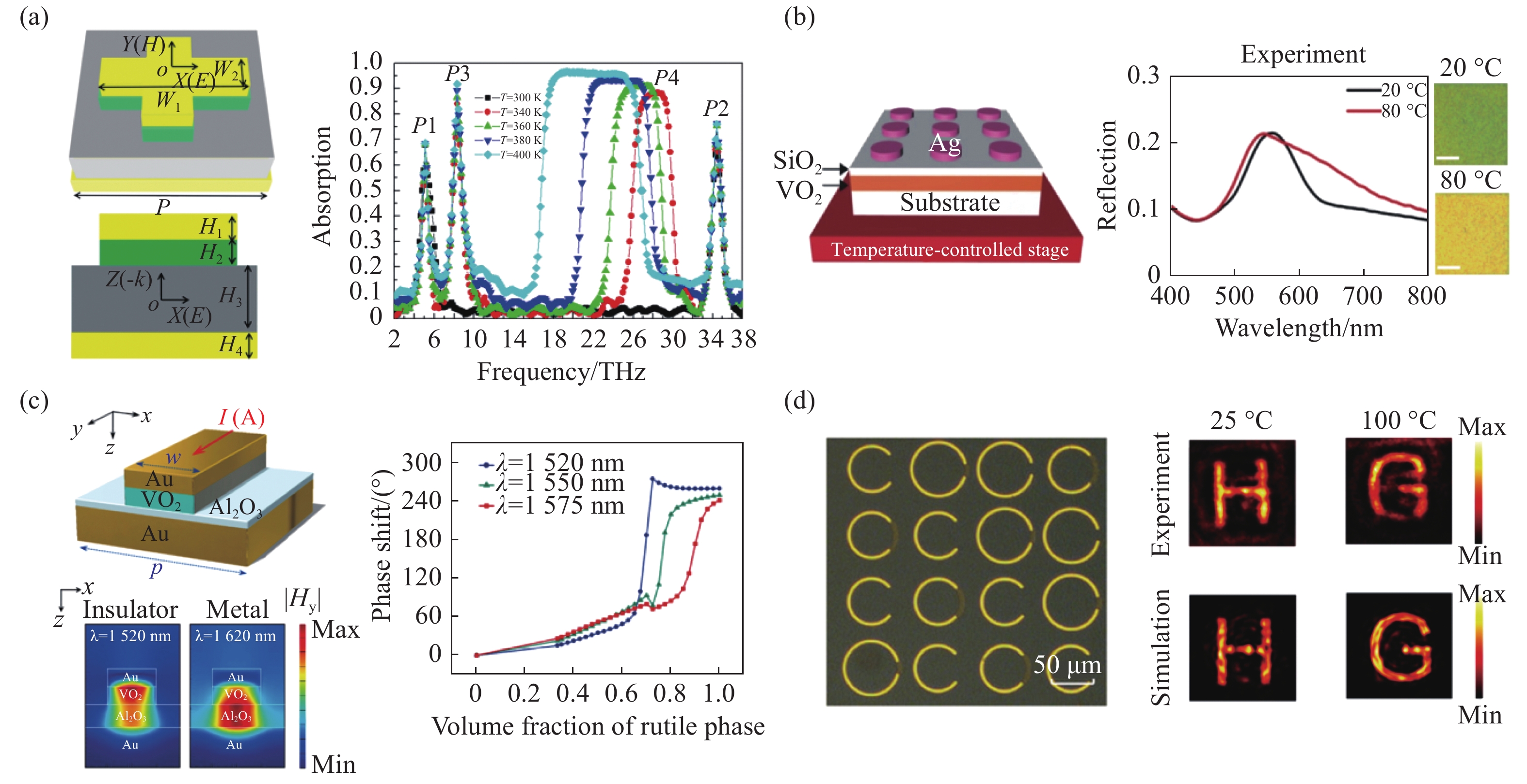
图 1 VO2基热驱动可调谐光学超构材料。(a) THz波段可调谐吸收器示意图(左)及其实验测得的温控吸收谱线(右)[23]。(b)可见光波段反射式可调谐光学超构表面的示意图(左)及其在20 ℃和80 ℃下测得的反射光谱和颜色显示图(右),比例尺为30 μm[25]。(c)反射式相位可调谐光学超构表面示意图(左上)及其在1520 nm和1620 nm波长处的磁场分布(左下);超构材料的相位调控与电压的关系谱线(右)[20]。(d) THz波段温控动态全息超构表面及其在25 ℃和100 ℃时的实验(右上)和模拟(右下)全息图像[19]
Figure 1. Thermally-driven tunable optical metamaterials based on VO2. (a) Schematic of a tunable absorber in the THz region (left) and the measured temperature dependent absorption spectra (right)[23]. (b) Schematic of a tunable optical metasurface in the visible region (left) and the measured reflection spectra and observed colors at 20 ℃ and 80 ℃, accordingly (right), scale bar: 30 μm[25]. (c) Schematic of a phase-tunable optical metasurface (top left) and the simulated magnetic field distributions at the two wavelengths of 1520 nm and 1620 nm, respectively (bottom left); the relationship between phase shift of metamaterials and external voltage (right)[20]. (d) A temperature-controlled dynamic holographic metasurface in the THz region[19] and the measured (upper right) and simulated (lower right) holographic images at 25 ℃ and 100 ℃

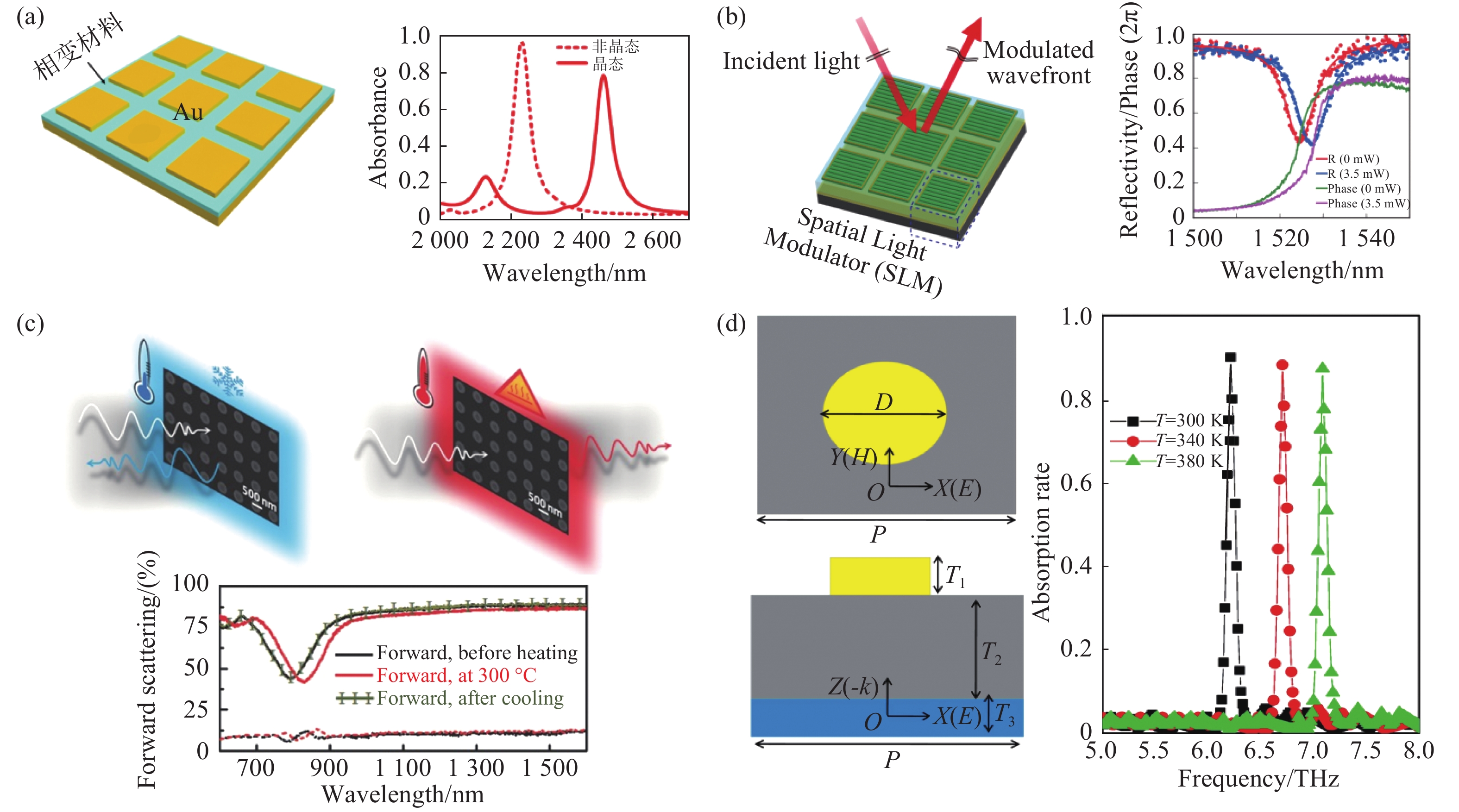
图 2 热驱动可调谐光学超构材料。(a)基于相变材料的可调谐完美吸波器示意图及相变材料处于非晶态或晶态时模拟得到的吸收光谱[32]。(b)电热驱动的硅基空间光调制器的示意图及其在3.5 mW的电驱动下的相位、振幅调制谱线[47]。(c)温控硅基可调谐光学超构表面示意图及其温控可调谐的散射光谱特性[48]。(d)基于SrTiO3的可调谐吸波器的结构示意图,其中黄色部分为金属层,灰色部分为光刻胶层(SU-8),蓝色部分为SrTiO3层(左),实验测得的温控吸收光谱(右)[51]
Figure 2. Thermally-driven tunable optical metamaterials. (a) Schematic of a tunable perfect absorber based on phase change material and the simulated absorption spectra of the absorber with the structural states of amorphous and crystalline[32]. (b) Schematic of an electrothermally-driven silicon-based spatial light modulator and its modulation spectra of phase and amplitude under a driving power of 3.5 mW[47]. (c) Schematic of a temperature-controlled silicon-based tunable optical metasurface and its scattering spectra[48]. (d) Schematic of the meta-atom of SrTiO3-based tunable absorber, where the yellow, gray, blue parts represent the three layers of metal, photoresist (SU-8), and SrTiO3, accordingly (left). The measured temperature-controlled absorption spectra in the THz region (right)[51]

图 3 液晶基和二极管基电驱动可调谐超构材料。(a) 液晶基透射式可调谐超构表面操控光束示意图(上),实验测得的三个主要衍射级的透射谱(下)[56]。(b)偏振敏感的超构材料示意图(上左)以及液晶基偏振敏感的电控可调谐超构材料(上右),0~5 V电压驱动和入射偏振光共同作用下的颜色调制光学照片(下)[57]。(c)二极管基可调谐超构材料反射器的示意图(左)以及实验测得的不同电压驱动下的反射谱(右)[60]。(d)二极管基时空编码超构表面示意图[61]
Figure 3. The electrically-driven tunable metamaterials based on liquid crystal and diode, respectively. (a) Schematic of a liquid crystal based transmissive metasurface for beam steering(top), the measured transmission spectra of the three main diffraction orders (bottom)[56]. (b) Schematic of polarization-sensitive metamaterials(top left) and liquid crystal based polarization-sensitive electrically-controlled tunable metamaterials (top right), color modulation with the combination of 0~5 V external voltage and polarization states of incident light (bottom)[57]. (c) Schematic of a diode-based tunable metamaterial reflector (left) and the measured reflection spectra with the different external voltages (right)[60]. (d) Schematic of the diode-based space-time coding metasurface[61]

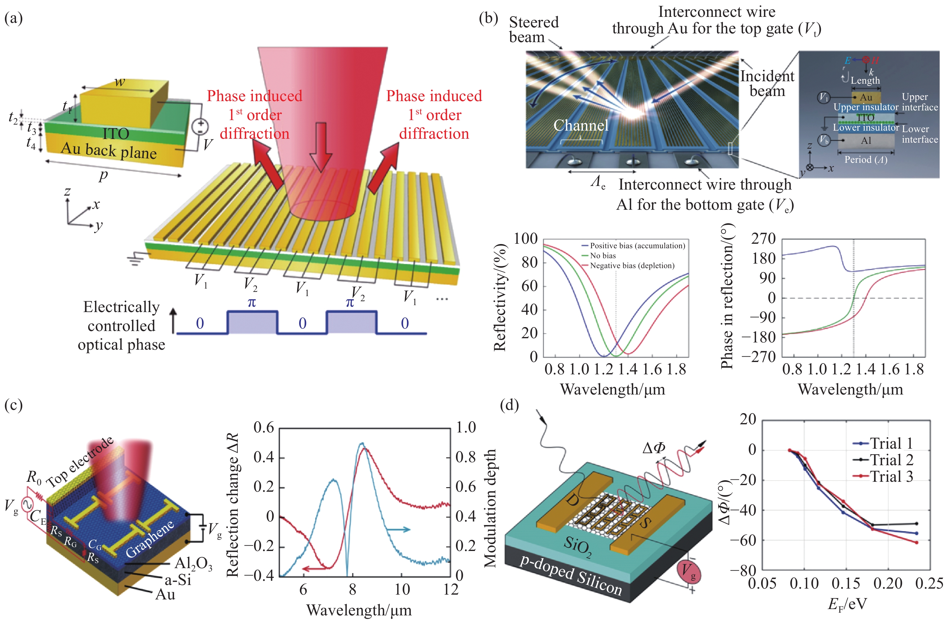
图 4 ITO基和石墨烯基电驱动可调谐光学超构材料。(a)电控ITO基相位可调谐超构材料示意图[65]。(b) ITO基相位和振幅解耦调谐的超构表面示意图(左上),结构单元示意图(右上)及其电控可调谐的反射光谱(左下)和相位调制光谱(右下)[68]。(c)石墨烯基可调谐超构表面示意图(左)及栅极偏压相关的调制深度光谱(右)[75]。(d)基于单层石墨烯的相位可调谐超构材料示意图(左)及实验测得的不同石墨烯费米能级下超构材料的相位调制曲线(右)[76]
Figure 4. The electrically-driven tunable optical metamaterials based on ITO and graphene, respectively. (a) Schematic of an electrically-controlled ITO-based phase tunable metamaterials[65]. (b) Schematic of a ITO-based tunable metasurface with decoupling modulation of phase and amplitude (top left), schematic of meta-atom (top right) and its electrically-controlled reflection spectra (bottom left) and phase shift spectra(bottom right)[68]. (c) Schematic of a graphene-based tunable metasurface (left) and gate bias voltage related modulation depth spectra (right)[75]. (d) Schematic of a phase-tunable metamaterial based on single-layer graphene (left) and the measured phase modulation curves of metamaterials at the different graphene Fermi levels (right)[76]

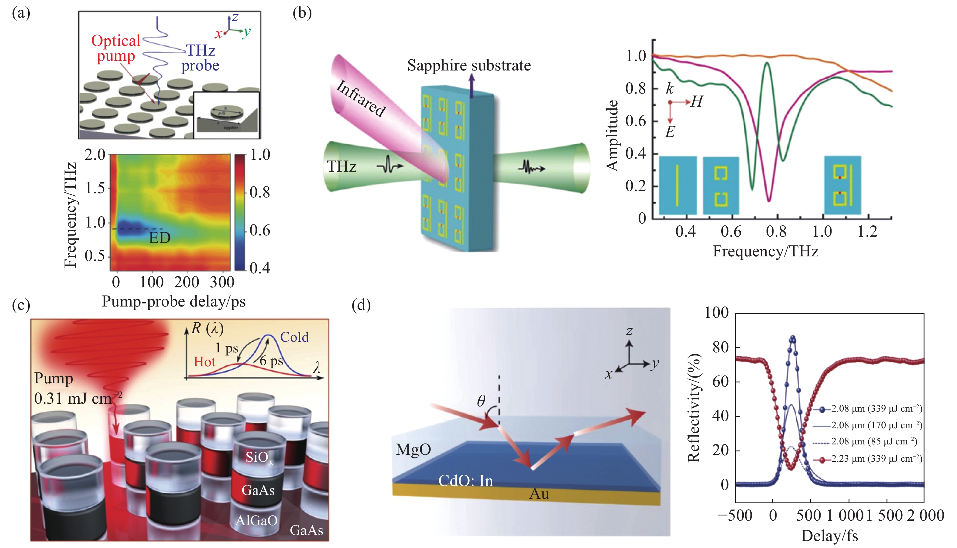
图 5 光驱动可调谐光学超构材料。(a) 硅基光控可调谐超构表面示意图(上)及其在不同延迟的飞秒激光激励下的透射调制响应(下)[77]。(b)光驱动硅基EIT可调谐超构材料示意图(左),单线结构(粉红色)、双开口谐振环结构(橙色)和EIT超构材料(橄榄色)的透射振幅光谱[78]。(c)低泵浦光驱动的GaAs 基可调谐超构表面示意图[80]。(d)基于CdO:In材料的全光偏振开关器件示意图(左)及其在亚带隙泵浦光照射下的p偏振光反射谱[81]
Figure 5. Light-driven tunable optical metamaterials. (a) Schematic of a tunable metasurface integrated with silicon elements (top) and the transmittance modulation response under femtosecond laser excitation with the different delay (bottom)[77]. (b) Schematic of silicon-based EIT tunable metamaterials (left), the transmission spectra of cutting wire structure (pink), double-splitting resonance ring structure (orange) and EIT metamaterial (olive)[78]. (c) Schematic of GaAs-based tunable metasurface pumped with a low light power[80]. (d) Schematic of all-optical polarization switching device based on CdO:In material (left) and the reflection spectra of p-polarized light under sub-band gap pumping light irradiation[81]

图 6 磁驱动可调谐光学超构材料。(a) 磁等离子超构材料示意图(左)及其在饱和磁场作用下,纵向磁光强度效应δ的频谱幅值谱线(右),蓝线为计算值,红线为实验值[85]。(b)由金属和磁光材料混合构成的光束偏转超构表面示意图(左)及其在不同强度磁场作用下的光束偏转情况(右)[86]。(c) 以磁性物质Ce1Y2Fe5O12作为介质层的磁可调谐超构表面示意图(左)及其磁场可调手性成像效果(右)[87]。(d)以磁性物质镍作为圆盘结构的磁可调谐超构表面的扫描电子显微镜图像(左)及其在不同方向的磁场作用下的手性透射光谱(右)[88]
Figure 6. Magnetically-driven tunable optical metamaterials. (a) Schematic of the magnetic plasma metamaterial (left) and the spectra of longitudinal magneto-optical intensity effect δ with a saturated magnetic field (right), where simulated and measured spectra are shown in the blue and red curves, respectively[85]. (b) Schematic of a beam deflection metasurface composed of a mixture of metal and magneto-optical materials (left) and its beam deflection under different magnetic (H-) fields intensity (right)[86]. (c) Schematic of a magnetically tunable metasurface integrated with a magnetic material Ce1Y2Fe5O12 dielectric layer (left) and its H-field induced tunable chiral imaging effect (right)[87]. (d) Scanning electron microscope image (left) of a magnetically tunable metasurface integrated with magnetic dielectric Ni disk and its chiral transmission spectra with the magnetic fields in different directions (right)[88]

图 7 拉伸可调谐光学超构材料。(a) 基于PDMS基板的动态调谐结构示意图(左)以及超构材料在不同拉伸长度下的反射光谱(右)[95]。(b)可拉伸TiO2超构表面的示意图(左)及其在不同偏振状态下不同应变的反射光谱(右)[96]。(c)可拉伸基材上的超构表面全息图(左),在拉力作用下,该全息图从“皱着眉头”变为“笑脸”(右)[93]。(d)电控可调谐超构透镜的示意图(左),1 kV电压驱动下,超构透镜的焦距从50.1 mm变为53.1 mm(中)以及两个条件下焦点处的光场强度分布(右)[104]
Figure 7. Stretching tunable optical metamaterials. (a) Schematic of a dynamically tunable structure based on PDMS substrate (left) and reflection spectra of metamaterials under the different stretchable lengths (right)[95]. (b) Schematic of a stretchable TiO2 metasurface (left) and its reflection spectra of the different strains in the different polarization states (right)[96]. (c) Metasurface hologram on a stretchable substrate (left). Under the action of tension, the hologram changes from "frowning" to "smiling face" (right)[93]. (d) Schematic diagram of an electrically-controlled tunable metalens (left), the focal length changes from 50.1 mm to 53.1 mm (middle) under 1 kV voltage drive, and the light field intensity distributions at the focal point with two conditions (right)[104]

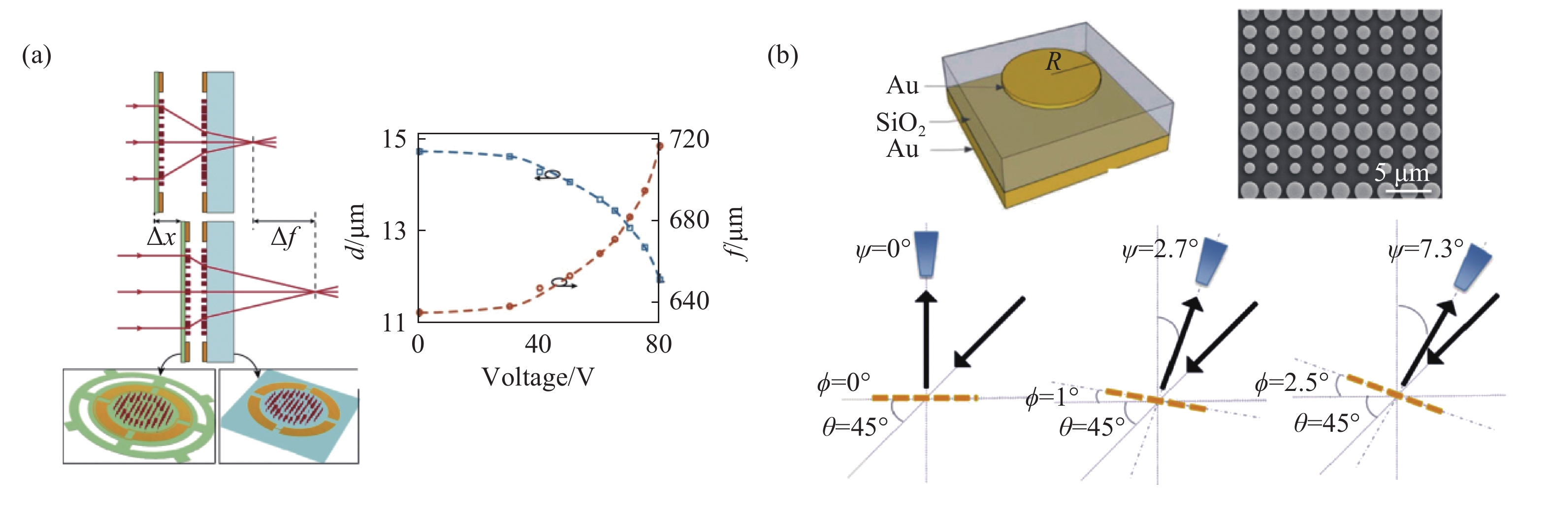
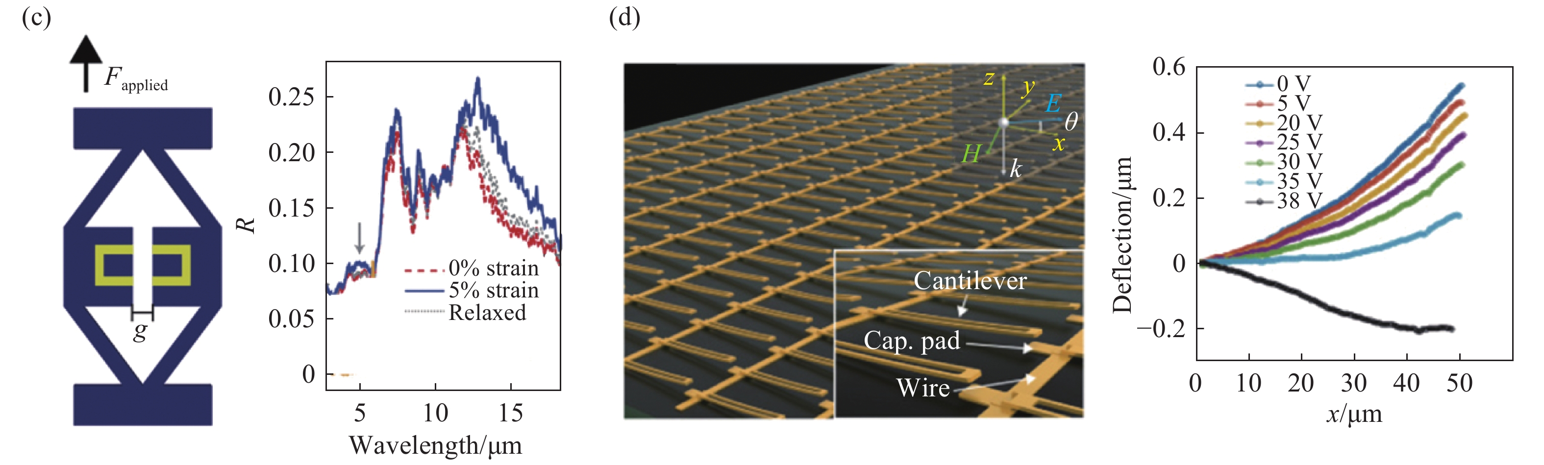
图 8 结构重构型可调谐光学超构材料。(a) MEMS可调超构透镜的示意图(左);实验测得的前焦距f和两个超构透镜之间距离d随施加的直流电压变化曲线(右)[18]。(b)超构表面透镜单元结构示意图(左上),超构透镜样品的扫描电子显微镜图像(右上)及其调制机制(下)[108]。(c)基于柔性聚合物支架的可拉伸电磁超构材料示意图(左),不同外力拉伸下超构表面的反射光谱(右)[114]。(d)由悬臂、电容垫和互连线组成的THz可调谐超构材料示意图(左)和不同电压下悬臂曲率偏转曲线(右)[115]
Figure 8. Reconfigurably tunable optical metamaterials. (a) Schematic of a MEMS tunable metalens (left); measured front focal length f and the distance d between two metalenses varying with external DC voltage (right)[18]. (b) Schematic of the meta-atom (top left), a scanning electron microscope image (top right) and the modulation mechanism (bottom) of the metalens[108]. (c) Schematic of a stretchable electromagnetic metamaterial based on a flexible polymer stent (left), and the reflection spectra of a metasurface under the different external forces (right)[114]. (d) Schematic of a tunable THz metamaterial composed of a cantilever, a capacitor pad and an interconnection line (left) and the deflection curve of the cantilever curvature under different voltages (right)[115]
-
[1] PENDRY J B, HOLDEN A J, STEWART W J, et al. Extremely low frequency plasmons in metallic mesostructures[J]. Physical Review Letters, 1996, 76(25): 4773-4776. doi: 10.1103/PhysRevLett.76.4773 [2] PENDRY J B. Negative refraction makes a perfect lens[J]. Physical Review Letters, 2000, 85(18): 3966-3969. doi: 10.1103/PhysRevLett.85.3966 [3] FANG N, LEE H, SUN CH, et al. Sub-diffraction-limited optical imaging with a silver superlens[J]. Science, 2005, 308(5721): 534-537. doi: 10.1126/science.1108759 [4] SCHURIG D, MOCK J J, JUSTICE B J, et al. Metamaterial electromagnetic cloak at microwave frequencies[J]. Science, 2006, 314(5801): 977-980. doi: 10.1126/science.1133628 [5] LIU R, JI C, MOCK J J, et al. Broadband ground-plane cloak[J]. Science, 2009, 323(5912): 366-369. doi: 10.1126/science.1166949 [6] MA H F, CUI T J. Three-dimensional broadband ground-plane cloak made of metamaterials[J]. Nature Communications, 2010, 1(3): 21. [7] ERGIN T, STENGER N, BRENNER P, et al. Three-dimensional invisibility cloak at optical wavelengths[J]. Science, 2010, 328(5976): 337-339. doi: 10.1126/science.1186351 [8] CUI T J, LI L L, LIU SH, et al. Information metamaterial systems[J]. iScience, 2020, 23(8): 101403. doi: 10.1016/j.isci.2020.101403 [9] ZHELUDEV N I, KIVSHAR Y S. From metamaterials to metadevices[J]. Nature Materials, 2012, 11(11): 917-924. doi: 10.1038/nmat3431 [10] REN ZH H, CHANG Y H, MA Y M, et al. Leveraging of MEMS technologies for optical metamaterials applications[J]. Advanced Optical Materials, 2020, 8(3): 1900653. doi: 10.1002/adom.201900653 [11] CHEN H T, TAYLOR A J, YU N F. A review of metasurfaces: physics and applications[J]. Reports on Progress in Physics, 2016, 79(7): 076401. doi: 10.1088/0034-4885/79/7/076401 [12] HE Q, SUN SH L, ZHOU L. Tunable/reconfigurable metasurfaces: physics and applications[J]. Research, 2019, 2019: 1849272. [13] CHE Y H, WANG X T, SONG Q H, et al. Tunable optical metasurfaces enabled by multiple modulation mechanisms[J]. Nanophotonics, 2020, 9(15): 4407-4431. doi: 10.1515/nanoph-2020-0311 [14] CUI T, BAI B F, SUN H B. Tunable metasurfaces based on active materials[J]. Advanced Functional Materials, 2019, 29(10): 1806692. doi: 10.1002/adfm.201806692 [15] CHANG Y H, WEI J X, LEE C. Metamaterials-from fundamentals and MEMS tuning mechanisms to applications[J]. Nanophotonics, 2020, 9(10): 3049-3070. doi: 10.1515/nanoph-2020-0045 [16] MENG K, PARK S J, LI L H, et al. Tunable broadband terahertz polarizer using graphene-metal hybrid metasurface[J]. Optics Express, 2019, 27(23): 33768-33778. doi: 10.1364/OE.27.033768 [17] ZHANG J, WEI X ZH, RUKHLENKO I D, et al. Electrically tunable metasurface with independent frequency and amplitude modulations[J]. ACS Photonics, 2020, 7(1): 265-271. doi: 10.1021/acsphotonics.9b01532 [18] ARBABI E, ARBABI A, KAMALI S M, et al. MEMS-tunable dielectric metasurface lens[J]. Nature Communications, 2018, 9: 812. doi: 10.1038/s41467-018-03155-6 [19] LIU X B, WANG Q, ZHANG X Q, et al. Thermally dependent dynamic meta‐holography using a vanadium dioxide integrated metasurface[J]. Advanced Optical Materials, 2019, 7(12): 1900175. doi: 10.1002/adom.201900175 [20] KIM Y, WU P C, SOKHOYAN R, et al. Phase modulation with electrically tunable vanadium dioxide phase-change metasurfaces[J]. Nano Letters, 2019, 19(6): 3961-3968. doi: 10.1021/acs.nanolett.9b01246 [21] LEI D Y, APPAVOO K, LIGMAJER F, et al. Optically-triggered nanoscale memory effect in a hybrid plasmonic-phase changing nanostructure[J]. ACS Photonics, 2015, 2(9): 1306-1313. doi: 10.1021/acsphotonics.5b00249 [22] HAIL C U, MICHEL A K U, POULIKAKOS D, et al. Optical metasurfaces: evolving from passive to adaptive[J]. Advanced Optical Materials, 2019, 7(14): 1801786. doi: 10.1002/adom.201801786 [23] ZHONG M. A multi-band metamaterial absorber based on VO2 layer[J]. Optics &Laser Technology, 2021, 139: 106930. [24] KATS M A, SHARMA D, LIN J, et al. Ultra-thin perfect absorber employing a tunable phase change material[J]. Applied Physics Letters, 2012, 101(22): 221101. doi: 10.1063/1.4767646 [25] SHU F ZH, YU F F, PENG R W, et al. Dynamic plasmonic color generation based on phase transition of vanadium dioxide[J]. Advanced Optical Materials, 2018, 6(7): 1700939. doi: 10.1002/adom.201700939 [26] HASHEMI M R M, YANG SH H, WANG T Y, et al. Electronically-controlled beam-steering through vanadium dioxide metasurfaces[J]. Scientific Reports, 2016, 6: 35439. doi: 10.1038/srep35439 [27] ZHU M, COJOCARU‐MIRÉDIN O, MIO A M, et al. Unique bond breaking in crystalline phase change materials and the quest for metavalent bonding[J]. Advanced Materials, 2018, 30(18): 1706735. doi: 10.1002/adma.201706735 [28] DING F, YANG Y Q, BOZHEVOLNYI S I. Dynamic metasurfaces using phase‐change chalcogenides[J]. Advanced Optical Materials, 2019, 7(14): 1801709. doi: 10.1002/adom.201801709 [29] JEONG Y G, BAHK Y M, KIM D S. Dynamic terahertz plasmonics enabled by phase-change materials[J]. Advanced Optical Materials, 2020, 8(3): 1900548. doi: 10.1002/adom.201900548 [30] WUTTIG M, YAMADA N. Phase-change materials for rewriteable data storage[J]. Nature Materials, 2007, 6(11): 824-832. doi: 10.1038/nmat2009 [31] CAO T, WANG R Z, SIMPSON R E, et al. Photonic Ge-Sb-Te phase change metamaterials and their applications[J]. Progress in Quantum Electronics, 2020, 74: 100299. doi: 10.1016/j.pquantelec.2020.100299 [32] CAO T, ZHANG L, SIMPSON R E, et al. Mid-infrared tunable polarization-independent perfect absorber using a phase-changing metamaterial[J]. Journal of the Optical Society of America B, 2013, 30(6): 1580-1585. [33] GHOLIPOUR B, ZHANG J F, MACDONALD K F, et al. An all-optical, non-volatile, bidirectional, phase-change meta-switch[J]. Advanced Materials, 2013, 25(22): 3050-3054. doi: 10.1002/adma.201300588 [34] TITTL A, MICHEL A K U, SCHÄFERLING M, et al. A switchable mid-infrared plasmonic perfect absorber with multispectral thermal imaging capability[J]. Advanced Materials, 2015, 27(31): 4597-4603. doi: 10.1002/adma.201502023 [35] QU Y R, LI Q, DU K K, et al. Dynamic thermal emission control based on ultrathin plasmonic metamaterials including phase-changing material GST[J]. Laser &Photonics Reviews, 2017, 11(5): 1700091. [36] BEHERA J K, LIU K, LIAN M, et al. A reconfigurable hyperbolic metamaterial perfect absorber[J]. Nanoscale Advances, 2021, 3(6): 1758-1766. doi: 10.1039/D0NA00787K [37] CAO T, LIU K, LU L, et al. Large-area broadband near-perfect absorption from a thin chalcogenide film coupled to gold nanoparticles[J]. ACS Applied Materials &Interfaces, 2019, 11(5): 5176-5182. [38] JULIAN M N, WILLIAMS C, BORG S, et al. Reversible optical tuning of GeSbTe phase-change metasurface spectral filters for mid-wave infrared imaging[J]. Optica, 2020, 7(7): 746-754. doi: 10.1364/OPTICA.392878 [39] DE GALARRETA C R, SINEV I, ALEXEEV A M, et al. Reconfigurable multilevel control of hybrid all-dielectric phase-change metasurfaces[J]. Optica, 2020, 7(5): 476-484. doi: 10.1364/OPTICA.384138 [40] WANG Y F, LANDREMAN P, SCHOEN D, et al. Electrical tuning of phase-change antennas and metasurfaces[J]. Nature Nanotechnology, 2021. doi: 10.1038/s41565-021-00882-8 [41] ZHANG Y F, FOWLER C, LIANG J H, et al. Electrically reconfigurable non-volatile metasurface using low-loss optical phase-change material[J]. Nature Nanotechnology, 2021. doi: 10.1038/s41565-021-00881-9 [42] HOSSEINI P, WRIGHT C D, BHASKARAN H. An optoelectronic framework enabled by low-dimensional phase-change films[J]. Nature, 2014, 511(7508): 206-211. doi: 10.1038/nature13487 [43] YOO S, GWON T, EOM T, et al. Multicolor changeable optical coating by adopting multiple layers of ultrathin phase change material film[J]. ACS Photonics, 2016, 3(7): 1265-1270. doi: 10.1021/acsphotonics.6b00246 [44] DE GALARRETA C R, ALEXEEV A M, AU Y Y, et al. Nonvolatile reconfigurable phase‐change metadevices for beam steering in the near infrared[J]. Advanced Functional Materials, 2018, 28(10): 1704993. doi: 10.1002/adfm.201704993 [45] BAI W, YANG P, HUANG J, et al. Near-infrared tunable metalens based on phase change material Ge2Sb2Te5[J]. Scientific Reports, 2019, 9(1): 5368. doi: 10.1038/s41598-019-41859-x [46] STAUDE I, SCHILLING J. Metamaterial-inspired silicon nanophotonics[J]. Nature Photonics, 2017, 11(5): 274-284. doi: 10.1038/nphoton.2017.39 [47] HORIE Y, ARBABI A, ARBABI E, et al. High-speed, phase-dominant spatial light modulation with silicon-based active resonant antennas[J]. ACS Photonics, 2018, 5(5): 1711-1717. doi: 10.1021/acsphotonics.7b01073 [48] RAHMANI M, XU L, MIROSHNICHENKO A E, et al. Reversible thermal tuning of all-dielectric metasurfaces[J]. Advanced Functional Materials, 2017, 27(31): 1700580. doi: 10.1002/adfm.201700580 [49] NGUYEN Q M, ANTHONY T K, ZAGHLOUL A I. Free-Space-Impedance-Matched composite dielectric metamaterial with high refractive index[J]. IEEE Antennas and Wireless Propagation Letters, 2019, 18(12): 2751-2755. doi: 10.1109/LAWP.2019.2951122 [50] CHEN X, FAN W H. Tunable bound states in the continuum in all-dielectric terahertz metasurfaces[J]. Nanomaterials, 2020, 10(4): 623. doi: 10.3390/nano10040623 [51] ZHONG M, JIANG X T, ZHU X L, et al. Design and fabrication of a single metal layer tunable metamaterial absorber in THz range[J]. Optics &Laser Technology, 2020, 125: 106023. [52] MA Z, MENG X, LIU X, et al. Liquid crystal enabled dynamic nanodevices[J]. Nanomaterials, 2018, 8(11): 871. [53] SI G Y, ZHAO Y H, LEONG E S P, et al. Liquid-crystal-enabled active plasmonics: a review[J]. Materials, 2014, 7(2): 1296-1317. doi: 10.3390/ma7021296 [54] KOMAR A, FANG ZH, BOHN J, et al. Electrically tunable all-dielectric optical metasurfaces based on liquid crystals[J]. Applied Physics Letters, 2017, 110(7): 071109. doi: 10.1063/1.4976504 [55] ATORF B, MÜHLENBERND H, MULDARISNUR M, et al. Electro-optic tuning of split ring resonators embedded in a liquid crystal[J]. Optics Letters, 2014, 39(5): 1129-1132. doi: 10.1364/OL.39.001129 [56] LI SH Q, XU X W, VEETIL R M, et al. Phase-only transmissive spatial light modulator based on tunable dielectric metasurface[J]. Science, 2019, 364(6445): 1087-1090. doi: 10.1126/science.aaw6747 [57] SHARMA M, HENDLER N, ELLENBOGEN T. Electrically switchable color tags based on active liquid‐crystal plasmonic metasurface platform[J]. Advanced Optical Materials, 2020, 8(7): 1901182. doi: 10.1002/adom.201901182 [58] FRANKLIN D, FRANK R, WU S T, et al. Actively addressed single pixel full-colour plasmonic display[J]. Nature Communications, 2017, 8: 15209. doi: 10.1038/ncomms15209 [59] AMER A A G, SAPUAN S Z, NASIMUDDIN N, et al. A comprehensive review of metasurface structures suitable for RF energy harvesting[J]. IEEE Access, 2020, 8: 76433-76452. doi: 10.1109/ACCESS.2020.2989516 [60] XU W R, SONKUSALE S. Microwave diode switchable metamaterial reflector/absorber[J]. Applied Physics Letters, 2013, 103(3): 031902. doi: 10.1063/1.4813750 [61] ZHANG L, CHEN X Q, LIU SH, et al. Space-time-coding digital metasurfaces[J]. Nature Communications, 2018, 9(1): 4334. doi: 10.1038/s41467-018-06802-0 [62] CUI T J, QI M Q, WAN X, et al. Coding metamaterials, digital metamaterials and programmable metamaterials[J]. Light:Science &Applications, 2014, 3(10): e218. [63] LI L L, SHUANG Y, MA Q, et al. Intelligent metasurface imager and recognizer[J]. Light:Science &Applications, 2019, 8: 97. [64] LI L L, CUI T J, JI W, et al. Electromagnetic reprogrammable coding-metasurface holograms[J]. Nature Communications, 2017, 8(1): 197. doi: 10.1038/s41467-017-00164-9 [65] HUANG Y W, LEE H W H, SOKHOYAN R, et al. Gate-tunable conducting oxide metasurfaces[J]. Nano Letters, 2016, 16(9): 5319-5325. doi: 10.1021/acs.nanolett.6b00555 [66] SHIRMANESH G K, SOKHOYAN R, PALA R A, et al. Dual-gated active metasurface at 1550 nm with wide (> 300°) phase tunability[J]. Nano Letters, 2018, 18(5): 2957-2963. doi: 10.1021/acs.nanolett.8b00351 [67] FOROUZMAND A, SALARY M M, INAMPUDI S, et al. A tunable multigate indium-tin-oxide-assisted all-dielectric metasurface[J]. Advanced Optical Materials, 2018, 6(7): 1701275. doi: 10.1002/adom.201701275 [68] PARK J, JEONG B G, KIM S I, et al. All-solid-state spatial light modulator with independent phase and amplitude control for three-dimensional LiDAR applications[J]. Nature Nanotechnology, 2021, 16(1): 69-76. doi: 10.1038/s41565-020-00787-y [69] WANG F, ZHANG Y B, TIAN CH SH, et al. Gate-variable optical transitions in graphene[J]. Science, 2008, 320(5873): 206-209. doi: 10.1126/science.1152793 [70] LI Z Q, HENRIKSEN E A, JIANG Z, et al. Dirac charge dynamics in graphene by infrared spectroscopy[J]. Nature Physics, 2008, 4(7): 532-535. doi: 10.1038/nphys989 [71] YAO Y, SHANKAR R, KATS M A, et al. Electrically tunable metasurface perfect absorbers for ultrathin mid-infrared optical modulators[J]. Nano Letters, 2014, 14(11): 6526-6532. doi: 10.1021/nl503104n [72] BONACCORSO F, SUN Z, HASAN T, et al. Graphene photonics and optoelectronics[J]. Nature Photonics, 2010, 4(9): 611-622. doi: 10.1038/nphoton.2010.186 [73] SHERROTT M C, HON P W C, FOUNTAINE K T, et al. Experimental demonstration of > 230° phase modulation in gate-tunable graphene–gold reconfigurable mid-infrared metasurfaces[J]. Nano Letters, 2017, 17(5): 3027-3034. doi: 10.1021/acs.nanolett.7b00359 [74] FAN K B, SUEN J, WU X Y, et al. Graphene metamaterial modulator for free-space thermal radiation[J]. Optics Express, 2016, 24(22): 25189-25201. doi: 10.1364/OE.24.025189 [75] ZENG B B, HUANG ZH Q, SINGH A, et al. Hybrid graphene metasurfaces for high-speed mid-infrared light modulation and single-pixel imaging[J]. Light:Science &Applications, 2018, 7: 51. [76] DABIDIAN N, DUTTA-GUPTA S, KHOLMANOV I, et al. Experimental demonstration of phase modulation and motion sensing using graphene-integrated metasurfaces[J]. Nano Letters, 2016, 16(6): 3607-3615. doi: 10.1021/acs.nanolett.6b00732 [77] CAI H L, HUANG Q P, HU X, et al. All‐optical and ultrafast tuning of terahertz plasmonic metasurfaces[J]. Advanced Optical Materials, 2018, 6(14): 1800143. doi: 10.1002/adom.201800143 [78] GU J Q, SINGH R, LIU X J, et al. Active control of electromagnetically induced transparency analogue in terahertz metamaterials[J]. Nature Communications, 2012, 3: 1151. doi: 10.1038/ncomms2153 [79] YANG Y M, KAMARAJU N, CAMPIONE S, et al. Transient GaAs plasmonic metasurfaces at terahertz frequencies[J]. ACS Photonics, 2017, 4(1): 15-21. doi: 10.1021/acsphotonics.6b00735 [80] SHCHERBAKOV M R, LIU SH, ZUBYUK V V, et al. Ultrafast all-optical tuning of direct-gap semiconductor metasurfaces[J]. Nature Communications, 2017, 8: 17. doi: 10.1038/s41467-017-00019-3 [81] YANG Y M, KELLEY K, SACHET E, et al. Femtosecond optical polarization switching using a cadmium oxide-based perfect absorber[J]. Nature Photonics, 2017, 11(6): 390-395. doi: 10.1038/nphoton.2017.64 [82] CHANANA A, LIU X J, ZHANG CH, et al. Ultrafast frequency-agile terahertz devices using methylammonium lead halide perovskites[J]. Science Advances, 2018, 4(5): eaar7353. doi: 10.1126/sciadv.aar7353 [83] MANJAPPA M, SRIVASTAVA Y K, SOLANKI A, et al. Hybrid lead halide perovskites for ultrasensitive photoactive switching in terahertz metamaterial devices[J]. Advanced Materials, 2017, 29(32): 1605881. doi: 10.1002/adma.201605881 [84] KUMAR A, SOLANKI A, MANJAPPA M, et al. Excitons in 2D perovskites for ultrafast terahertz photonic devices[J]. Science Advances, 2020, 6(8): eaax8821. doi: 10.1126/sciadv.aax8821 [85] BELOTELOV V I, KREILKAMP L E, AKIMOV I A, et al. Plasmon-mediated magneto-optical transparency[J]. Nature Communications, 2013, 4: 2128. doi: 10.1038/ncomms3128 [86] TAN ZH Y, FAN F, LI T F, et al. Magnetically active terahertz wavefront control and superchiral field in a magneto-optical Pancharatnam-Berry metasurface[J]. Optics Express, 2021, 29(2): 2037-2048. doi: 10.1364/OE.414004 [87] QIN J, DENG L J, KANG T T, et al. Switching the optical chirality in magnetoplasmonic metasurfaces using applied magnetic fields[J]. ACS Nano, 2020, 14(3): 2808-2816. doi: 10.1021/acsnano.9b05062 [88] ZUBRITSKAYA I, MACCAFERRI N, EZEIZA X I, et al. Magnetic control of the chiroptical plasmonic surfaces[J]. Nano Letters, 2018, 18(1): 302-307. doi: 10.1021/acs.nanolett.7b04139 [89] GUTRUF P, ZOU CH J, WITHAYACHUMNANKUL W, et al. Mechanically tunable dielectric resonator metasurfaces at visible frequencies[J]. ACS Nano, 2016, 10(1): 133-141. doi: 10.1021/acsnano.5b05954 [90] TSENG M L, YANG J, SEMMLINGER M, et al. Two-dimensional active tuning of an aluminum plasmonic array for full-spectrum response[J]. Nano Letters, 2017, 17(10): 6034-6039. doi: 10.1021/acs.nanolett.7b02350 [91] YOO D, JOHNSON T W, CHERUKULAPPURATH S, et al. Template-stripped tunable plasmonic devices on stretchable and rollable substrates[J]. ACS Nano, 2015, 9(11): 10647-10654. doi: 10.1021/acsnano.5b05279 [92] MORITS D, MORITS M, OVCHINNIKOV V, et al. Multifunctional stretchable metasurface for the THz range[J]. Journal of Optics, 2014, 16(3): 032001. doi: 10.1088/2040-8978/16/3/032001 [93] MALEK S C, EE H S, AGARWAL R. Strain multiplexed metasurface holograms on a stretchable substrate[J]. Nano Letters, 2017, 17(6): 3641-3645. doi: 10.1021/acs.nanolett.7b00807 [94] KAMALI S M, ARBABI A, ARBABI E, et al. Decoupling optical function and geometrical form using conformal flexible dielectric metasurfaces[J]. Nature Communications, 2016, 7: 11618. doi: 10.1038/ncomms11618 [95] SONG SH CH, MA X L, PU M B, et al. Actively tunable structural color rendering with tensile substrate[J]. Advanced Optical Materials, 2017, 5(9): 1600829. doi: 10.1002/adom.201600829 [96] ZHANG CH, JING J X, WU Y K, et al. Stretchable all-dielectric metasurfaces with polarization-insensitive and full-spectrum response[J]. ACS Nano, 2020, 14(2): 1418-1426. doi: 10.1021/acsnano.9b08228 [97] HUANG F M, BAUMBERG J J. Actively tuned plasmons on elastomerically driven Au nanoparticle dimers[J]. Nano Letters, 2010, 10(5): 1787-1792. doi: 10.1021/nl1004114 [98] CHEN W X, LIU W J, JIANG Y J, et al. Ultrasensitive, mechanically responsive optical metasurfaces via strain amplification[J]. ACS Nano, 2018, 12(11): 10683-10692. doi: 10.1021/acsnano.8b04889 [99] PRYCE I M, AYDIN K, KELAITA Y A, et al. Highly strained compliant optical metamaterials with large frequency tunability[J]. Nano Letters, 2010, 10(10): 4222-4227. doi: 10.1021/nl102684x [100] LIU X, HUANG ZH, ZHU CH K, et al. Out-of-plane designed soft metasurface for tunable surface plasmon polariton[J]. Nano Letters, 2018, 18(2): 1435-1441. doi: 10.1021/acs.nanolett.7b05190 [101] GAO Y SH, FAN Y B, WANG Y J, et al. Nonlinear holographic all-dielectric metasurfaces[J]. Nano Letters, 2018, 18(12): 8054-8061. doi: 10.1021/acs.nanolett.8b04311 [102] WAN W W, GAO J, YANG X D. Metasurface holograms for holographic imaging[J]. Advanced Optical Materials, 2017, 5(21): 1700541. doi: 10.1002/adom.201700541 [103] KAMALI S M, ARBABI E, ARBABI A, et al. Highly tunable elastic dielectric metasurface lenses[J]. Laser &Photonics Reviews, 2016, 10(6): 1002-1008. [104] SHE A L, ZHANG SH Y, SHIAN S, et al. Adaptive metalenses with simultaneous electrical control of focal length, astigmatism, and shift[J]. Science Advances, 2018, 4(2): eaap9957. doi: 10.1126/sciadv.aap9957 [105] OPRIS D M. Polar elastomers as novel materials for electromechanical actuator applications[J]. Advanced Materials, 2018, 30(5): 1703678. doi: 10.1002/adma.201703678 [106] SKOV A L, YU L Y. Optimization techniques for improving the performance of silicone‐based dielectric elastomers[J]. Advanced Engineering Materials, 2018, 20(5): 1700762. doi: 10.1002/adem.201700762 [107] SHAH S I H, SARKAR A, PHON R, et al. Two‐dimensional electromechanically transformable metasurface with beam scanning capability using four independently controllable shape memory alloy axes[J]. Advanced Optical Materials, 2020, 8(22): 2001180. doi: 10.1002/adom.202001180 [108] ROY T, ZHANG SH Y, JUNG I W, et al. Dynamic metasurface lens based on MEMS technology[J]. APL Photonics, 2018, 3(2): 021302. doi: 10.1063/1.5018865 [109] LIU X L, PADILLA W J. Dynamic manipulation of infrared radiation with MEMS metamaterials[J]. Advanced Optical Materials, 2013, 1(8): 559-562. doi: 10.1002/adom.201300163 [110] FU Y H, LIU A Q, ZHU W M, et al. A micromachined reconfigurable metamaterial via reconfiguration of asymmetric split‐ring resonators[J]. Advanced Functional Materials, 2011, 21(18): 3589-3594. doi: 10.1002/adfm.201101087 [111] HU F R, QIAN Y X, LI ZH, et al. Design of a tunable terahertz narrowband metamaterial absorber based on an electrostatically actuated MEMS cantilever and split ring resonator array[J]. Journal of Optics, 2013, 15(5): 055101. doi: 10.1088/2040-8978/15/5/055101 [112] KAN T, ISOZAKI A, KANDA N, et al. Enantiomeric switching of chiral metamaterial for terahertz polarization modulation employing vertically deformable MEMS spirals[J]. Nature Communications, 2015, 6: 8422. [113] ZHU W M, LIU A Q, ZHANG X M, et al. Switchable magnetic metamaterials using micromachining processes[J]. Advanced Materials, 2011, 23(15): 1792-1796. doi: 10.1002/adma.201004341 [114] REEVES J B, JAYNE R K, STARK T J, et al. Tunable infrared metasurface on a soft polymer scaffold[J]. Nano Letters, 2018, 18(5): 2802-2806. doi: 10.1021/acs.nanolett.7b05042 [115] ZHAO X G, SCHALCH J, ZHANG J D, et al. Electromechanically tunable metasurface transmission waveplate at terahertz frequencies[J]. Optica, 2018, 5(3): 303-310. doi: 10.1364/OPTICA.5.000303 [116] NAIK G V, SCHROEDER J L, NI X J, et al. Titanium nitride as a plasmonic material for visible and near-infrared wavelengths[J]. Optical Materials Express, 2012, 2(4): 478-489. doi: 10.1364/OME.2.000478 [117] BANG S, KIM J, YOON G, et al. Recent advances in tunable and reconfigurable metamaterials[J]. Micromachines, 2018, 9(11): 560. doi: 10.3390/mi9110560 [118] KANG L, JENKINS R P, WERNER D H. Recent progress in active optical metasurfaces[J]. Advanced Optical Materials, 2019, 7(14): 1801813. doi: 10.1002/adom.201801813 [119] ZHANG X G, JIANG W X, JIANG H L, et al. An optically driven digital metasurface for programming electromagnetic functions[J]. Nature Electronics, 2020, 3(3): 165-171. doi: 10.1038/s41928-020-0380-5 -

 下载:
下载:


计量
- 文章访问数: 3733
- HTML全文浏览量: 1194
- PDF下载量: 708
- 被引次数: 0
