


-
摘要: 氮化硅材料提供了一种与CMOS兼容的集成光子平台,具有丰富的光学特性。通过调节相关制备参数,可以获得特定折射率的薄膜材料,且消光系数和非线性系数具有较大可调控范围。因此,氮化硅材料在薄膜光学、微纳平面光学、非线性集成光学等诸多领域具有广泛的应用前景。本文主要介绍氮化硅材料的光学特性及其在光学薄膜、微纳超构材料和硅光集成器件方面的研究现状,综述氮化硅材料在太阳能薄膜、可见光超构表面、光栅耦合器和非线性光波导等应用领域的研究概况。Abstract: Silicon nitride provides a CMOS-compatible integrated photonic platform with rich optical properties. By adjusting the relevant fabrication parameters, silicon nitride with specific refractive index between 1.9~3.2 can be achieved, and its extinction and nonlinear coefficient can have a large adjustable range. Silicon nitride has wide potential applications in many fields such as thin film optics, micro-nano planar optics and nonlinear integrated photonics. In this paper, we review the optical properties of silicon nitride and its recent advances in optical film, micro-nano metamaterial and silicon photonics, and also review the research progresses on the applications of solar thin films, visible metasurfaces, grating couplers and nonlinear optical waveguides.
-
Key words:
- silicon nitride /
- metasurface /
- optical film /
- grating coupler /
- nonlinear optical waveguide
-
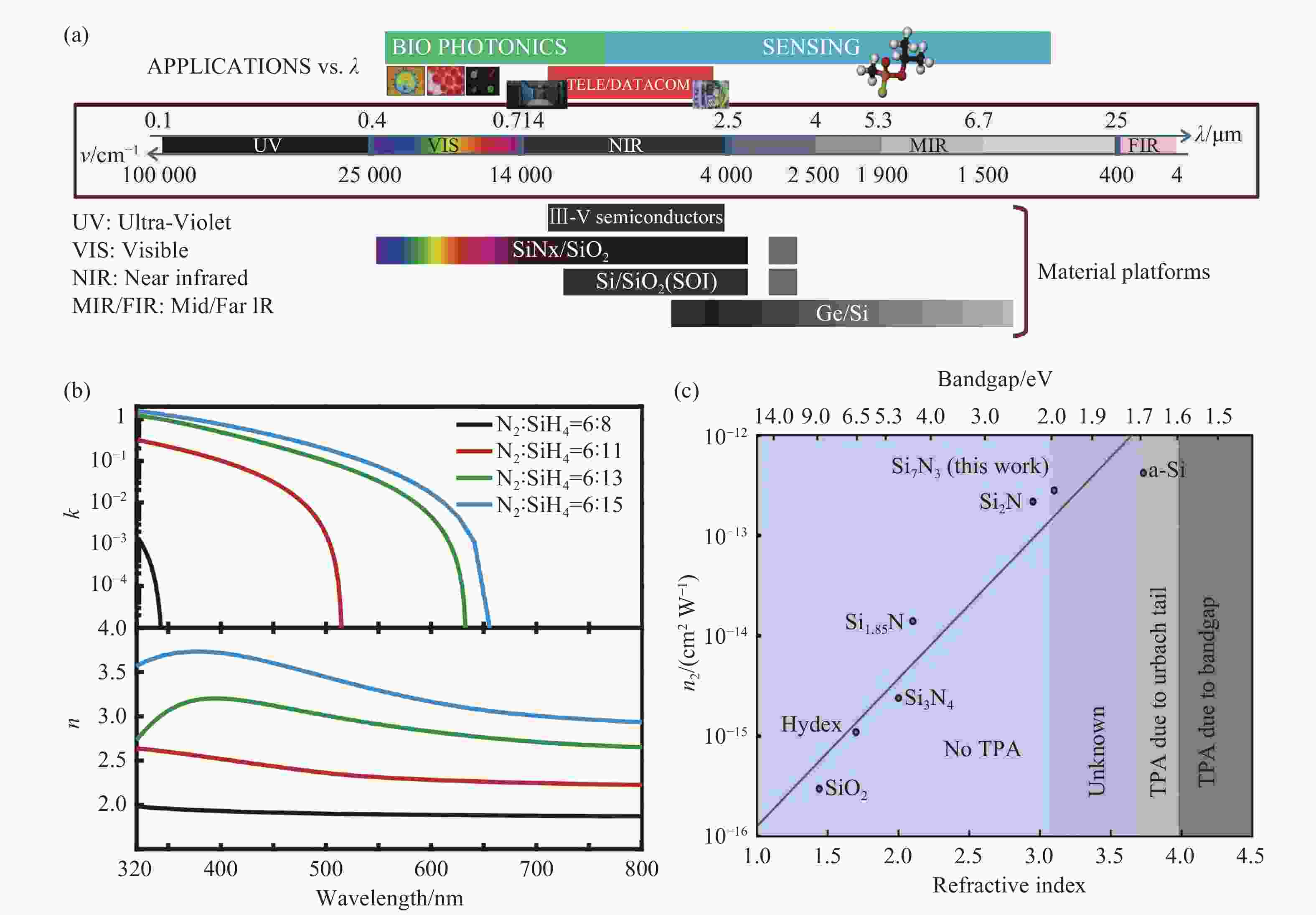
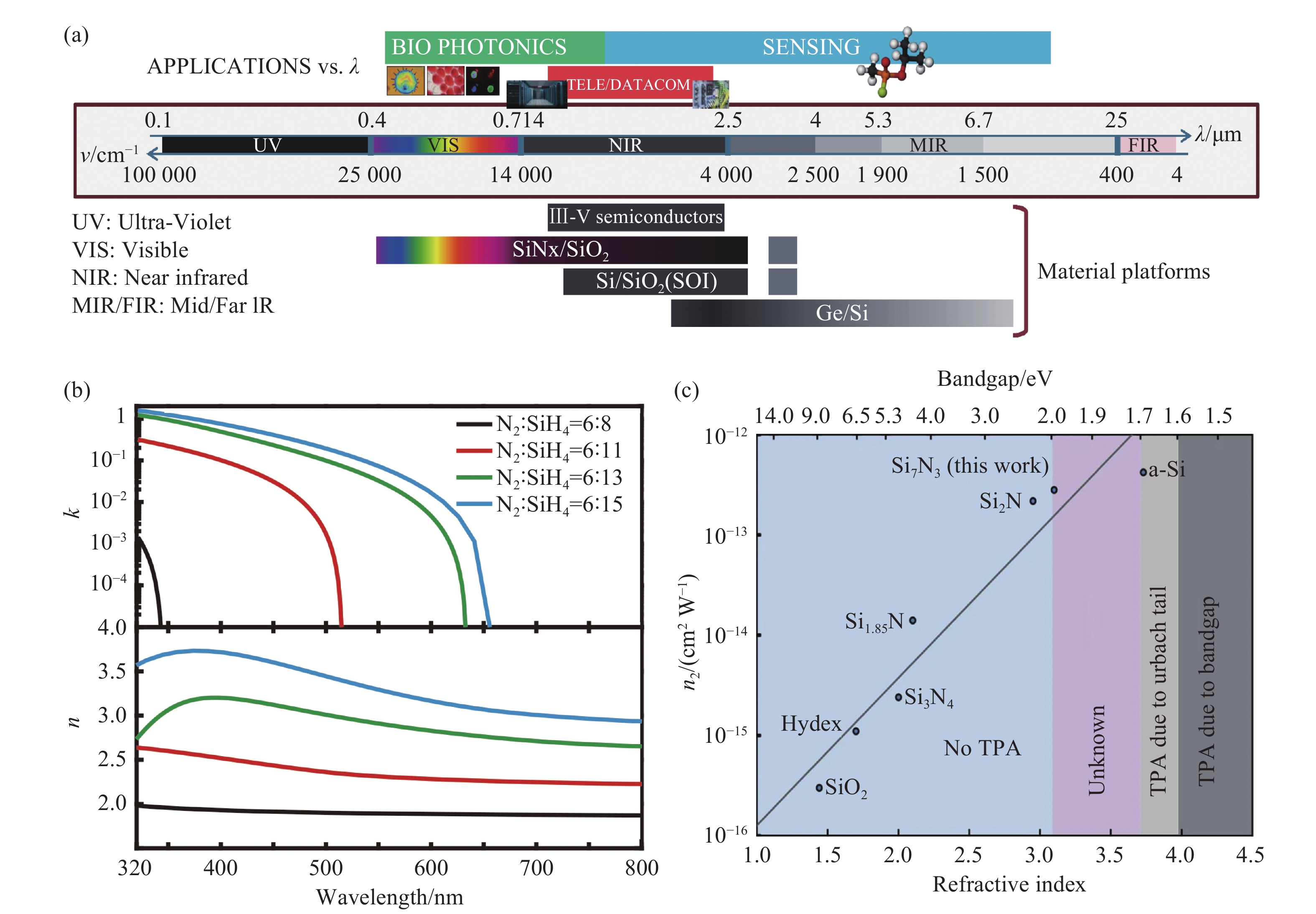
图 1 (a)不同材料体系在紫外到远红外的光谱工作波长范围以及对应波段的相关应用[11];(b)我们实验室中CVD沉积过程中通入不同N2/SiH4的气体浓度比例获得的氮化硅薄膜的光学参数(n,k)值;(c)二氧化硅、氮化硅以及硅材料的带隙与其(线性及非线性)折射率关系图[14]
Figure 1. (a) Working wavelengths of different material from UV to far-infrared and their related applications in corresponding wavebands[11]; (b) optical parameters (n, k) of silicon nitride films obtained by different N2/SiH4 gas concentration ratios during CVD by our lab; (c) diagram of the relationship between band gaps and (linear and nonlinear) refractive index of silicon dioxide, silicon nitride and silicon materials[14]
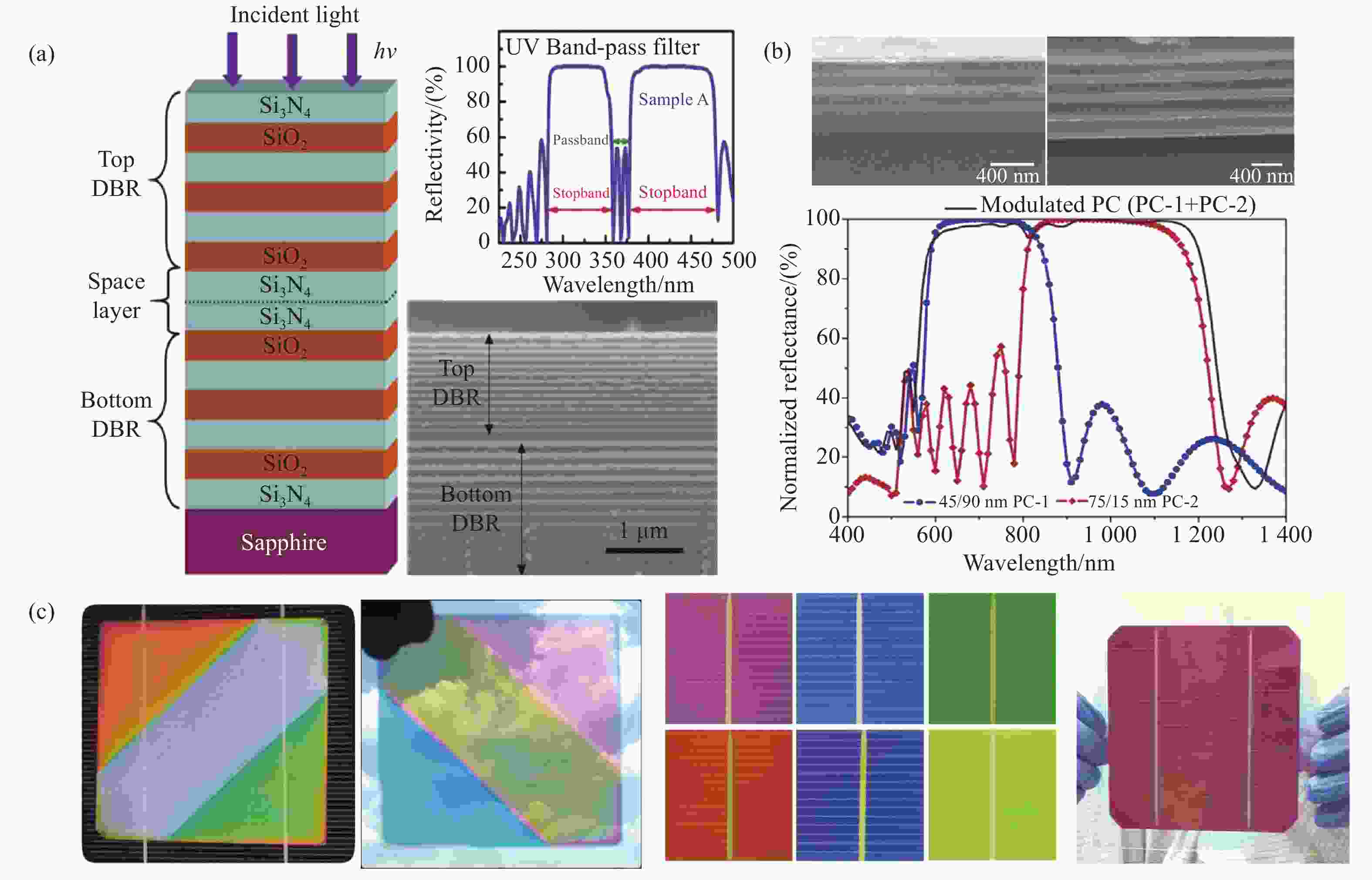
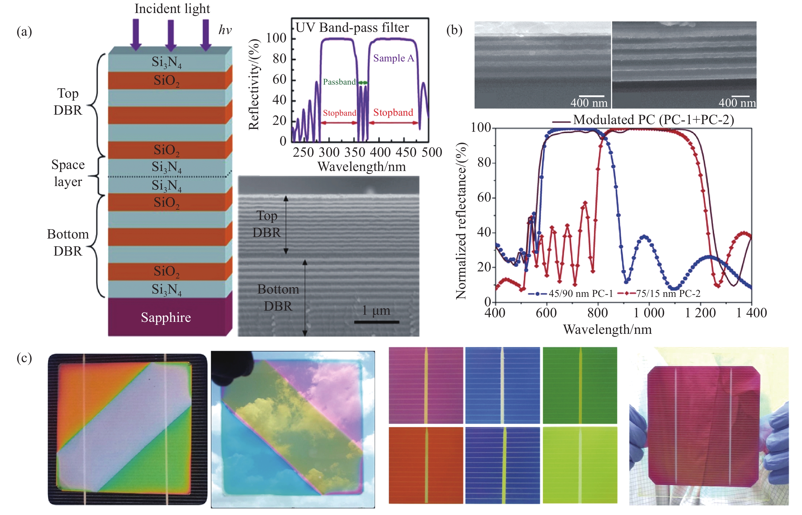
图 2 氮化硅均匀薄膜的光学应用。(a)带通滤波器结构图[15];(b)氮化硅/氮化硅/氮氧化硅多层减反射膜反射光谱及结构示意图[18];(c)氮化硅/氮氧化硅基彩色太阳能电池薄膜[19]
Figure 2. The optical application of silicon nitride homogeneous films. (a) Diagram of band-pass filter structure[15]; (b) reflection spectrum and structure diagram of silicon nitride / silicon nitride / silicon oxynitride multilayer antireflection film[18]; (c) silicon nitride / silicon oxynitride films in the application of colored solar cell[19]
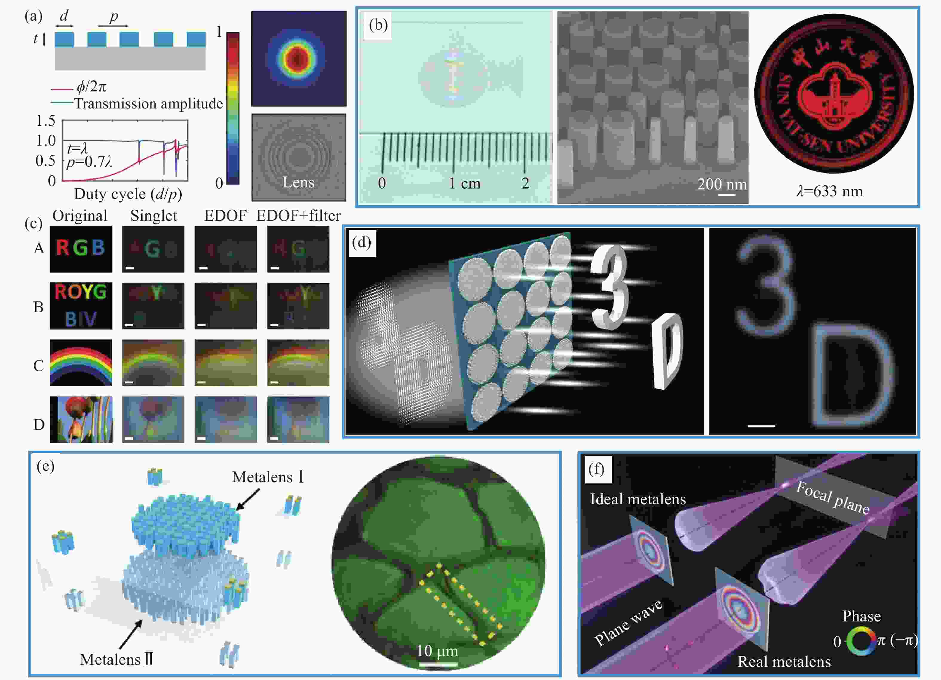
图 3 氮化硅超构透镜。(a)消球差氮化硅超构透镜实现接近衍射极限的聚焦性能[20];(b)高数值孔径厘米口径氮化硅超构透镜及其成像效果[12];(c)氮化硅超构透镜实现计算消色差成像[24];(d)氮化硅超构透镜阵列及其宽带消色差集成成像应用[26];(e)基于级联超构透镜的微型氮化硅超构物镜[28];(f)超构透镜相位测量[29]
Figure 3. Silicon nitride metalenses. (a) Spherical aberration free silicon nitride metalens achieves the nearly diffraction-limited focusing[20]; (b) high-NA centimeter-aperture silicon nitride metalens and its imaging performance[12]; (c) silicon nitride metalens for computational achromatic imaging[24]; (d) array of silicon nitride metalens for broadband achromatic integral imaging[26]; (e) microscope silicon nitride meta-objective based on cascaded metalenses[28]; (f) phase characterization of metalens[29]
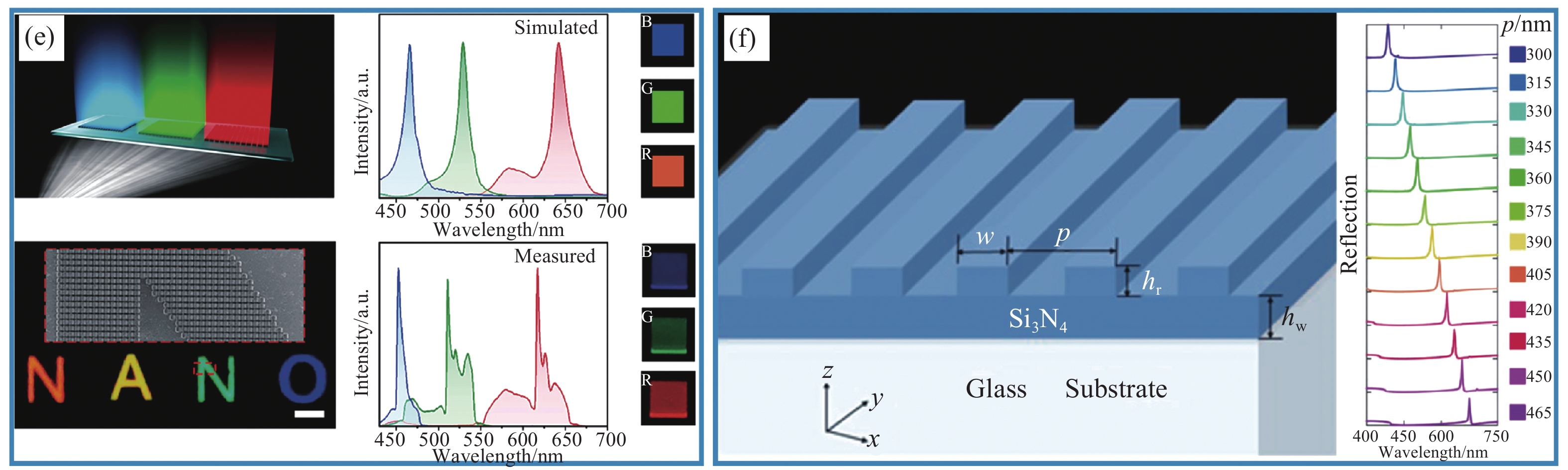
图 4 氮化硅颜色调控超构表面。(a)像素级RGB分色氮化硅超构表面[37];(b)氮化硅覆盖层的超构表面滤色片[38];(c)富硅氮化硅超构表面结构色测量光谱在CIE 1931色度图上的对应[39];(d)暗场下富硅氮化硅超构表面的反射颜色图[40];(e)像素级氮化硅超构表面实现结构色调控[41];(f)偏振敏感的一维氮化硅超构表面实现结构色调控[42]
Figure 4. Silicon nitride metasurfaces for color control. (a) Pixel-level RGB color separation silicon nitride metsurface[37]; (b) silicon nitride coating metasurface for color filter[38]; (c) the corresponding measurement spectrum of silicon-rich nitride metasurface on CIE 1931 chromaticity diagram[39]; (d) reflection colors of silicon-rich nitride metasurfaces in dark field[40]; (e) pixel-level silicon nitride metasurface for structural color controlling[41]; (f) one-dimensional polarization-sensitive silicon nitride metasurface for structural color controlling[42]

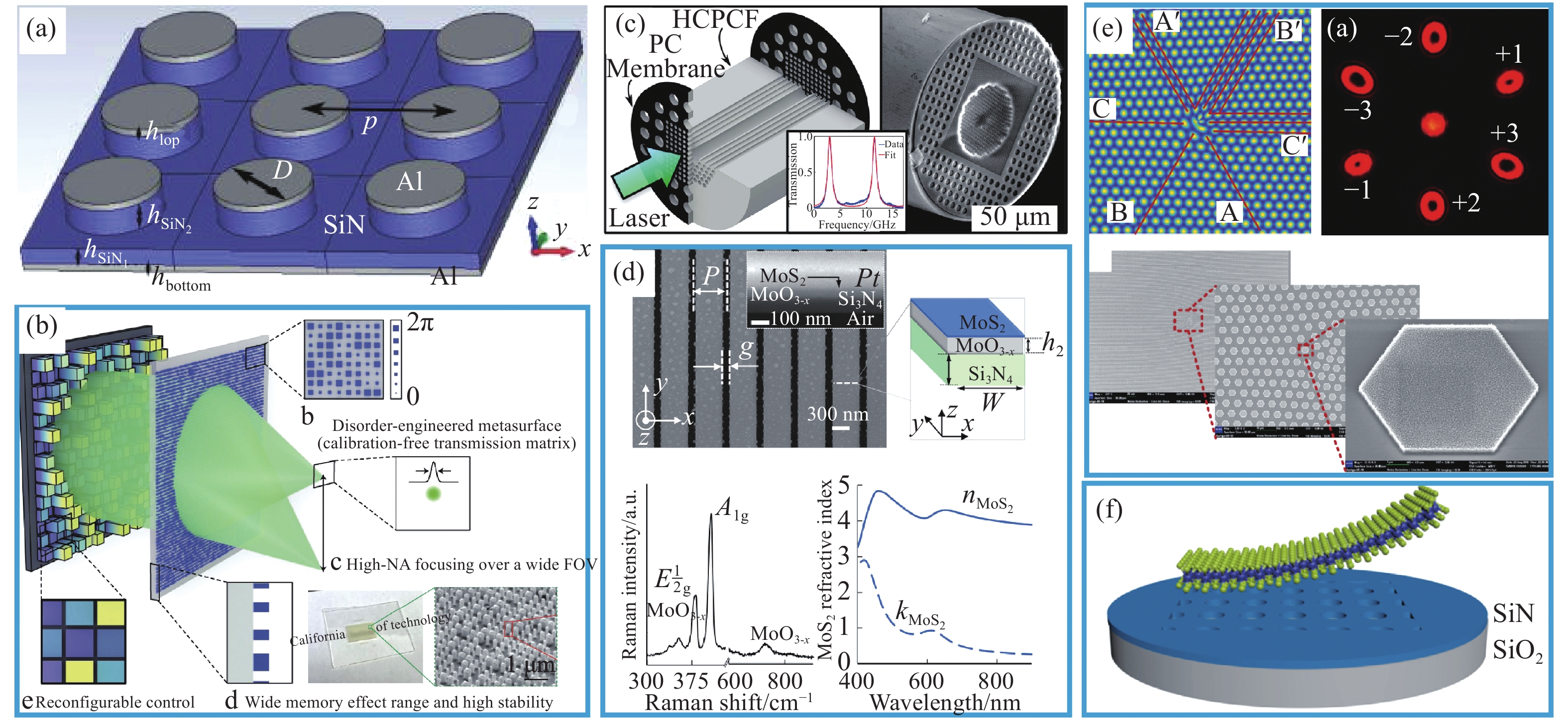
图 5 其它氮化硅超构表面。(a)长波红外氮化硅超构表面吸收器[43];(b)基于无序设计的氮化硅超构表面实现波前整形[44];(c)光纤端面氮化硅超构表面[45];(d)氮化硅超构表面实现机械变色[46];(e)多通道OAM氮化硅超构表面[47];(f)单层二硒化钨集成的氮化硅超构表面[50]
Figure 5. Other silicon nitride metasurfaces. (a) Silicon nitride metasurface absorber working on long-wave infrared[43]; (b) silicon nitride metasurface based on disordered design for wavefront shaping[44]; (c) silicon nitride metasurface at fiber end-face[45]; (d) mechanochromic reconfigurable silicon nitride metasurface[46]; (e) multi-channel OAM silicon nitride metasurface[47]; (f) silicon nitride metasurface integrated with single-layer WSe2[50]
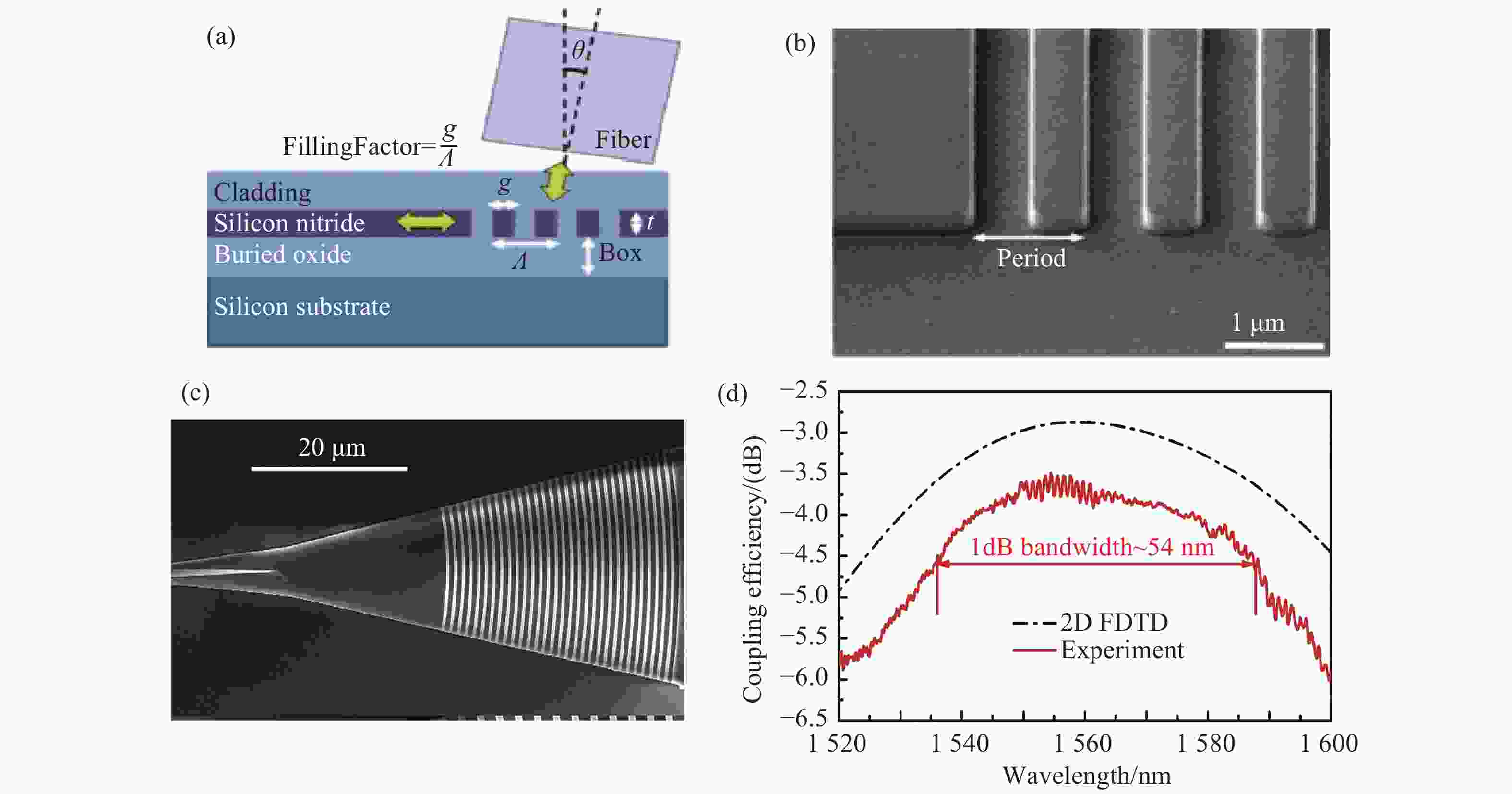
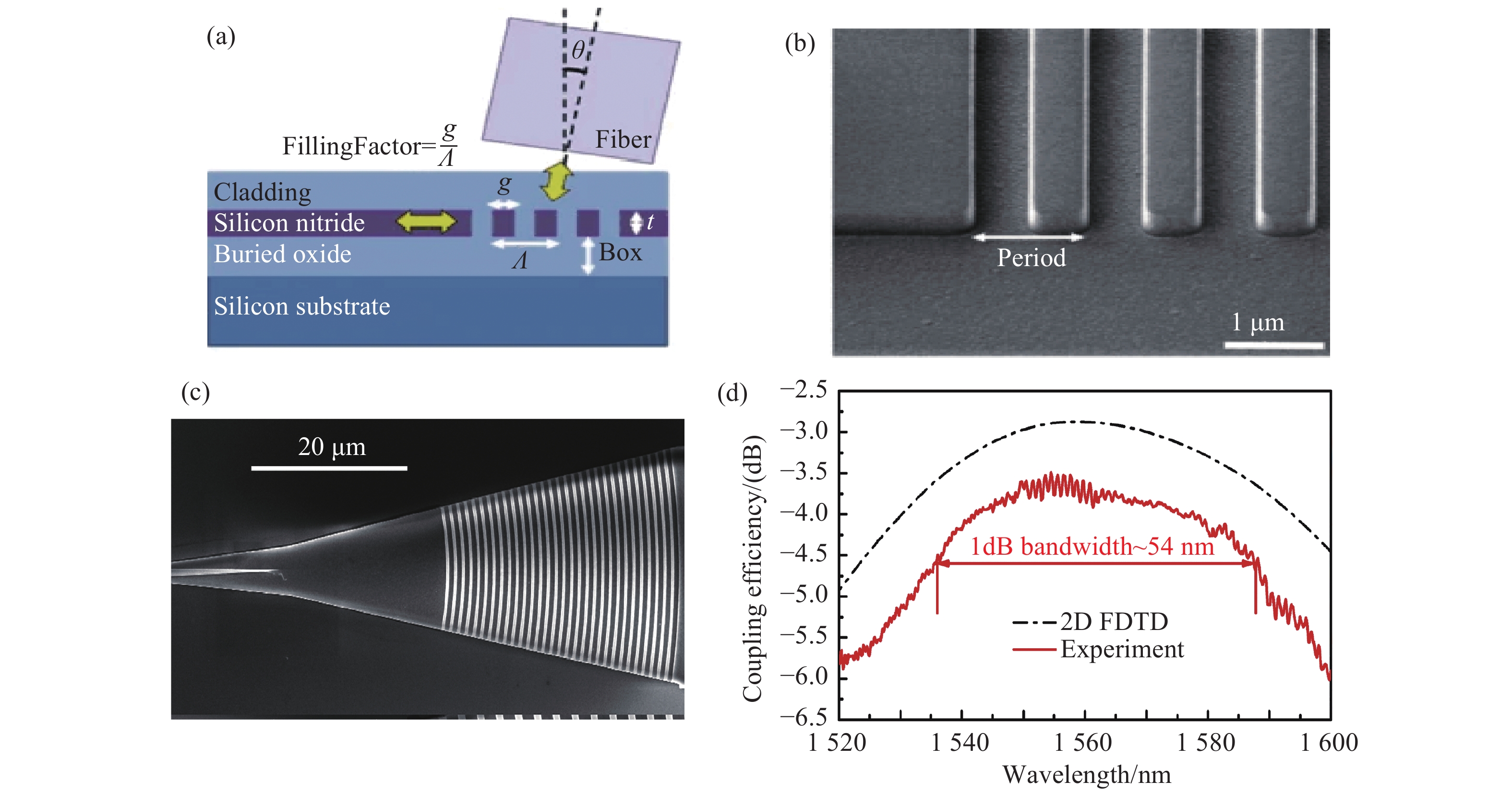
图 6 氮化硅单层光栅耦合器结构。(a)基于深紫外光刻制造的光栅耦合器示意图[60];(b)光栅耦合器部分区域放大的SEM图[60];(c)聚焦光栅耦合器结构的SEM图[61];(d)在不考虑拉锥波导损耗的情况下测得的氮化硅光栅耦合器的耦合效率(实线)和模拟的耦合效率(虚线)[61]
Figure 6. Silicon nitride single-layer grating couplers. (a) Schematic diagram of grating coupler manufactured based on deep ultraviolet lithography[60]; (b) enlarged SEM image of part of grating coupler[60]; (c) SEM image of focusing grating coupler structure[61]; (d) coupling efficiency (solid line) and simulated coupling efficiency (dashed line) of a silicon nitride grating coupler measured without considering the loss of the tapered waveguide[61]

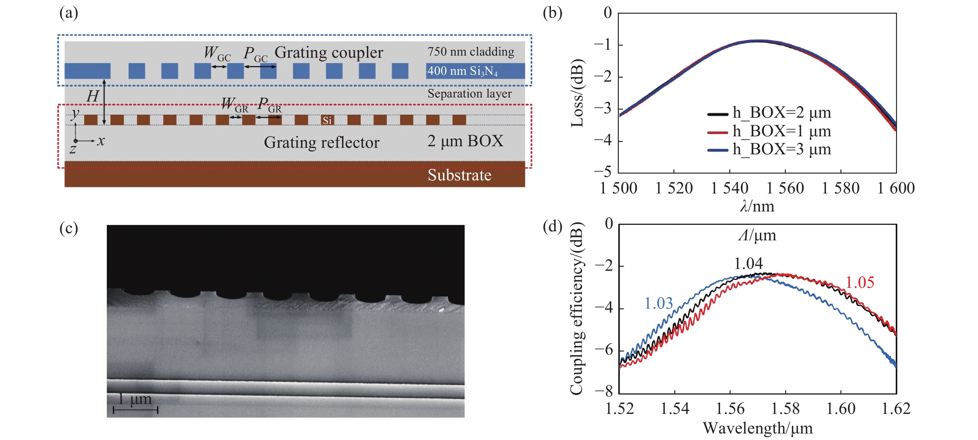
图 7 与底部反射镜相结合的氮化硅光栅耦合器。(a)以硅反射光栅作为底部反射镜的氮化硅光栅耦合器示意图[71];(b)具有不同掩埋氧化层厚度的变迹氮化硅光栅耦合器的耦合效率[71];(c)基于PECVD平台制造的DBR反射镜式部分刻蚀光栅耦合器SEM图[74];(d)光纤倾斜角为8.5°时不同光栅周期对耦合效率的影响[74]
Figure 7. Silicon nitride grating couplers combined with bottom mirror. (a) Schematic diagram of a silicon nitride grating coupler with a silicon reflection grating as the bottom mirror[71]; (b) coupling efficiency of apodized silicon nitride grating couplers with different buried oxide thicknesses[71]; (c) SEM image of DBR mirror type partially etched grating coupler manufactured on PECVD platform[74]; (d) the influence of different grating periods on the coupling efficiency when the fiber tilt angle is 8.5°[74]
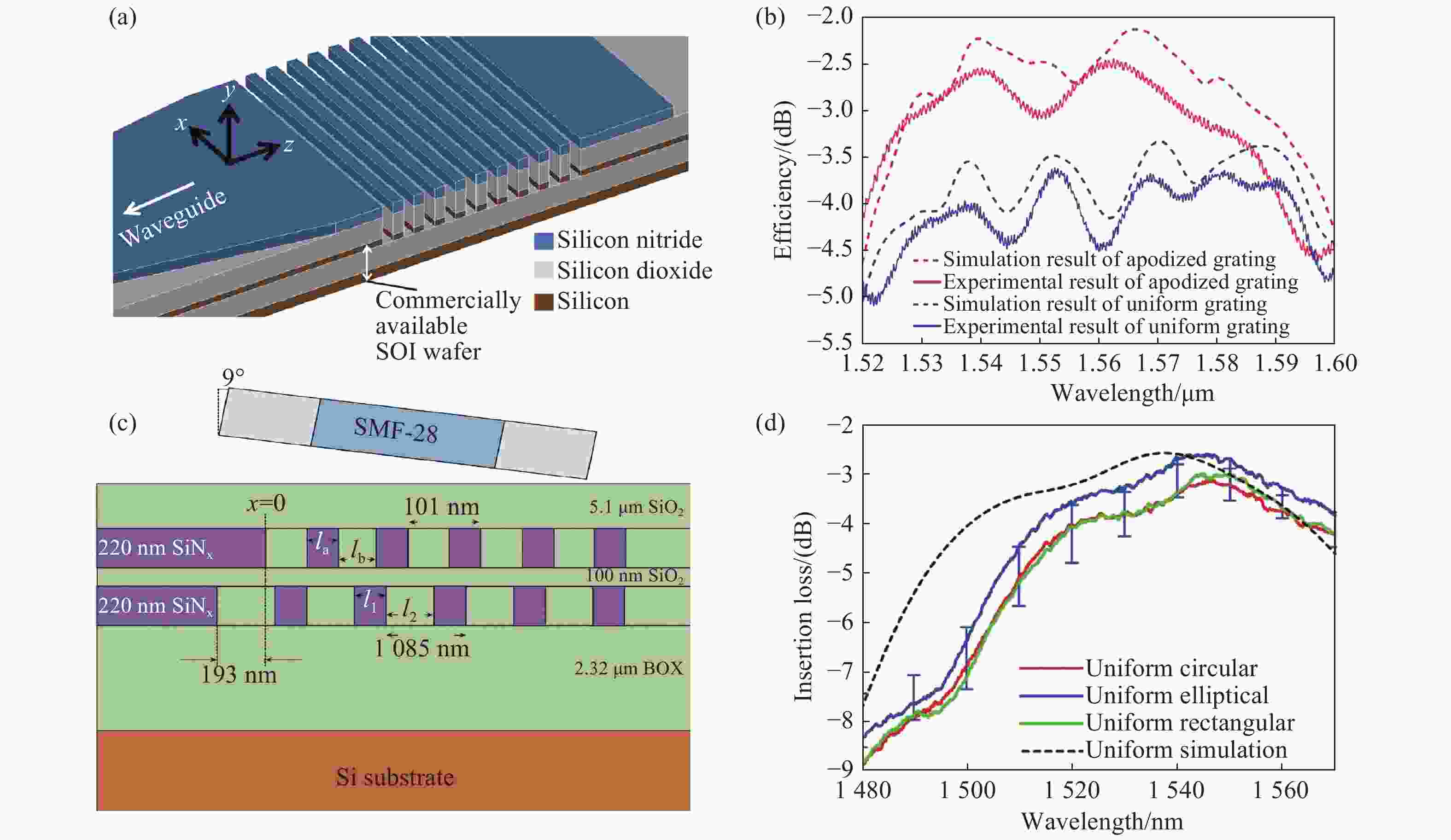
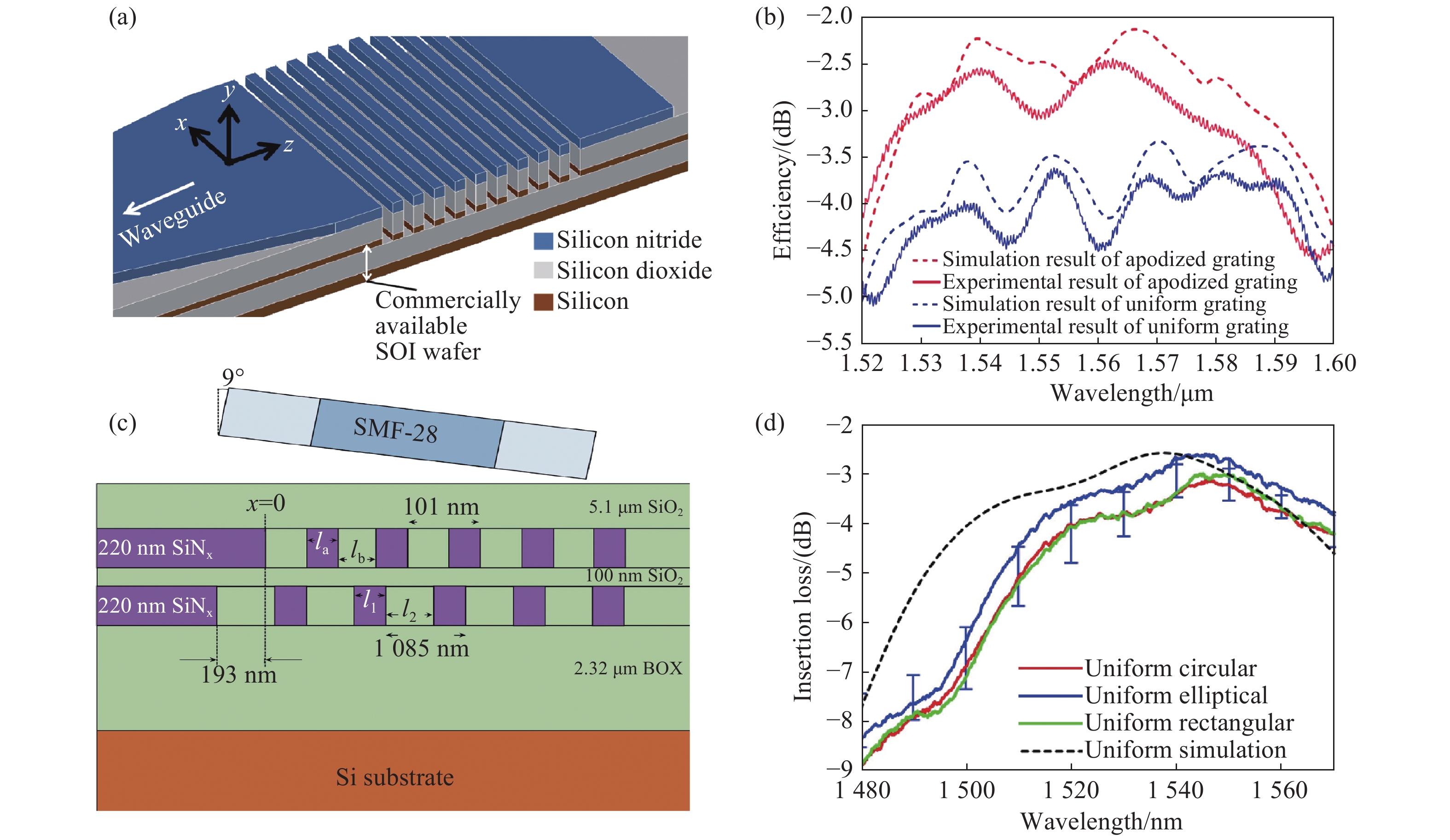
图 8 双层光栅耦合器。(a)由氮化硅光栅和硅光栅组成的双层光栅耦合器示意图[77];(b)均匀和变迹光栅耦合器模拟与实验测得的耦合效率曲线[77];(c)双层氮化硅光栅耦合器结构示意图[78];(d)对于具有不同横向布局(圆形,椭圆形和矩形)的光栅耦合器模拟和测量的耦合效率曲线。蓝色误差线表示椭圆布局的平均插入损耗的1个标准偏差[78]
Figure 8. Double-layer grating couplers. (a) Schematic diagram of double-layer grating coupler composed of silicon nitride grating and silicon grating[77]; (b) coupling efficiency curves of uniform and apodized grating couplers measured by simulation and experiment[77]; (c) schematic diagram of the double-layer silicon nitride grating coupler structure[78]; (d) simulated and measured coupling efficiency curves for grating couplers with different lateral layouts (circular, elliptical and rectangular). The blue error bar represents 1 standard deviation of the average insertion loss of the elliptical layout[78]

图 9 富硅氮化硅材料的非线性应用。(a)高垂直度低损耗富硅氮化硅波导实现波长转换[96];(b)富硅氮化硅光子晶体微腔获得二次与三次谐波[103];(c)富硅氮化硅谐振环结构观察到自相位调制获得光谱展宽[105]
Figure 9. Silicon-rich nitride materials for nonlinear applications. (a) High-perpendicularity and low-loss silicon-rich nitride waveguide for wavelength conversion[96]; (b) second and third harmonics generated by silicon-rich nitride photonic crystal cavity[103]; (c) spectral broadening obtained by self phase modulation in silicon-rich nitride micro ring resonator[105]
-
[1] 王正军. 氮化硅陶瓷的研究进展[J]. 材料科学与工艺,2009,17(2):155-158.WANG ZH J. Research progress of silicon nitride ceramic[J]. Materials Science &Technology, 2009, 17(2): 155-158. (in Chinese) [2] LANGE H, WÖTTING G, WINTER G. Silicon nitride—from powder synthesis to ceramic materials[J]. Angewandte Chemie International Edition in English, 1991, 30(12): 1579-1597. doi: 10.1002/anie.199115791 [3] DANTE R C, KAJDAS C K. A review and a fundamental theory of silicon nitride tribochemistry[J]. Wear, 2012, 288: 27-38. doi: 10.1016/j.wear.2012.03.001 [4] KALOYEROS A E, JOVÉ F A, GOFF J, et al. Review—silicon nitride and silicon nitride-rich thin film technologies: trends in deposition techniques and related applications[J]. ECS Journal of Solid State Science and Technology, 2017, 6(10): P691-P714. doi: 10.1149/2.0011710jss [5] BALÁZSI C, KÓNYA Z, WÉBER F, et al. Preparation and characterization of carbon nanotube reinforced silicon nitride composites[J]. Materials Science and Engineering:C, 2003, 23(6-8): 1133-1137. doi: 10.1016/j.msec.2003.09.085 [6] ŠAJGALIK P, DUSZA J, HOFFMANN M J. Relationship between microstructure, toughening mechanisms, and fracture toughness of reinforced silicon nitride ceramics[J]. Journal of the American Ceramic Society, 1995, 78(10): 2619-2624. doi: 10.1111/j.1151-2916.1995.tb08031.x [7] SCHMIDT S, HÄNNINEN T, GOYENOLA C, et al. SiNx coatings deposited by reactive high power impulse magnetron sputtering: process parameters influencing the nitrogen content[J]. ACS Applied Materials &Interfaces, 2016, 8(31): 20385-20395. [8] 邢武超. 高导热氮化硅陶瓷的低温制备及性能研究[D]. 郑州: 郑州航空工业管理学院, 2020.XING W CH. Study on low temperature preparation and properties of Silicon Nitride ceramics with high thermal conductivity[D]. Zhengzhou: Zhengzhou University of Aeronautics, 2020. (in Chinese) [9] RAIDER S I, FLITSCH R, ABOAF J A, et al. Surface oxidation of silicon nitride films[J]. Journal of the Electrochemical Society, 1976, 123(4): 560-565. doi: 10.1149/1.2132877 [10] LUBE T, DUSZA J. A silicon nitride reference material—A testing program of ESIS TC6[J]. Journal of the European Ceramic Society, 2007, 27(2-3): 1203-1209. doi: 10.1016/j.jeurceramsoc.2006.04.020 [11] MUÑOZ P, MICÓ G, BRU L A, et al. Silicon nitride photonic integration platforms for visible, near-infrared and mid-infrared applications[J]. Sensors, 2017, 17(9): 2088. doi: 10.3390/s17092088 [12] FAN ZH B, SHAO Z K, XIE M Y, et al. Silicon nitride metalenses for close-to-one numerical aperture and wide-angle visible imaging[J]. Physical Review Applied, 2018, 10(1): 014005. doi: 10.1103/PhysRevApplied.10.014005 [13] YE M, PENG Y H, YI Y SH. Silicon-rich silicon nitride thin films for subwavelength grating metalens[J]. Optical Materials Express, 2019, 9(3): 1200-1207. doi: 10.1364/OME.9.001200 [14] TAN D T H, OOI K J A, NG D K T. Nonlinear optics on silicon-rich nitride-a high nonlinear figure of merit CMOS platform [Invited][J]. Photonics Research, 2018, 6(5): B50-B66. doi: 10.1364/PRJ.6.000B50 [15] DAI J P, GAO W, LIU B, et al. Design and fabrication of UV band-pass filters based on SiO2/Si3N4 dielectric distributed bragg reflectors[J]. Applied Surface Science, 2016, 364: 886-891. doi: 10.1016/j.apsusc.2015.12.222 [16] LI J D, SHEN G S, CHEN W L, et al. Preparation of SiNx multilayer films by mid-frequency magnetron sputtering for crystalline silicon solar cells[J]. Materials Science in Semiconductor Processing, 2017, 59: 40-44. doi: 10.1016/j.mssp.2016.11.039 [17] SOMAN A, ANTONY A. Broad range refractive index engineering of SixNy and SiOxNy thin films and exploring their potential applications in crystalline silicon solar cells[J]. Materials Chemistry and Physics, 2017, 197: 181-191. doi: 10.1016/j.matchemphys.2017.05.035 [18] SOMAN A, ANTONY A. Tuneable and spectrally selective broadband reflector – Modulated photonic crystals and its application in solar cells[J]. Solar Energy, 2018, 162: 525-532. doi: 10.1016/j.solener.2018.01.061 [19] SOMAN A, ANTONY A. Colored solar cells with spectrally selective photonic crystal reflectors for application in building integrated photovoltaics[J]. Solar Energy, 2019, 181: 1-8. doi: 10.1016/j.solener.2019.01.058 [20] ZHAN A L, COLBURN S, TRIVEDI R, et al. Low-contrast dielectric metasurface optics[J]. ACS Photonics, 2016, 3(2): 209-214. doi: 10.1021/acsphotonics.5b00660 [21] ZHAO W, LI X Y, LI S Q, et al. Sub-wavelength focusing based on all-dielectric polarization-independent metalens[J]. International Journal of Modern Physics B, 2018, 32(29): 1850321. doi: 10.1142/S0217979218503216 [22] PARK J W, BAE S I, JEONG K H. Silicon nitride metalens for optical imaging[C]. 2018 International Conference on Optical MEMS and Nanophotonics (OMN), IEEE, 2018: 1-5. [23] YE M, RAY V, PENG Y H, et al. Linear polarization distinguishing metalens in visible wavelength[J]. Optics Letters, 2019, 44(2): 399-402. doi: 10.1364/OL.44.000399 [24] COLBURN S, ZHAN A L, MAJUMDAR A. Metasurface optics for full-color computational imaging[J]. Science Advances, 2018, 4(2): eaar2114. doi: 10.1126/sciadv.aar2114 [25] COLBURN S, MAJUMDAR A. Simultaneous achromatic and varifocal imaging with quartic metasurfaces in the visible[J]. ACS Photonics, 2020, 7(1): 120-127. doi: 10.1021/acsphotonics.9b01216 [26] FAN ZH B, QIU H Y, ZHANG H L, et al. A broadband achromatic metalens array for integral imaging in the visible[J]. Light:Science &Applications, 2019, 8: 67. [27] HUO Z H, PANG X N, WANG H, et al. Engineering the chromatic dispersion in dual-wavelength metalenses for unpolarized visible light[J]. Proceedings of SPIE, 2019, 11170: 111702H. [28] LIU Y, YU Q Y, CHEN Z M, et al. Meta-objective with sub-micrometer resolution for microendoscopes[J]. Photonics Research, 2021, 9(2): 106-115. doi: 10.1364/PRJ.406197 [29] ZHAO M X, CHEN M K, ZHUANG Z P, et al. Phase characterisation of metalenses[J]. Light:Science &Applications, 2021, 10(1): 52. [30] BAYATI E, PESTOURIE R, COLBURN S, et al. Inverse designed metalenses with extended depth of focus[J]. ACS Photonics, 2020, 7(4): 873-878. doi: 10.1021/acsphotonics.9b01703 [31] HUANG L CH, WHITEHEAD J, COLBURN S, et al. Design and analysis of extended depth of focus metalenses for achromatic computational imaging[J]. Photonics Research, 2020, 8(10): 1613-1623. doi: 10.1364/PRJ.396839 [32] ZHAN A L, COLBURN S, DODSON C M, et al. Metasurface freeform nanophotonics[J]. Scientific Reports, 2017, 7(1): 1673. doi: 10.1038/s41598-017-01908-9 [33] COLBURN S, ZHAN A L, MAJUMDAR A. Varifocal zoom imaging with large area focal length adjustable metalenses[J]. Optica, 2018, 5(7): 825-831. doi: 10.1364/OPTICA.5.000825 [34] HAN ZH Y, COLBURN S, MAJUMDAR A, et al. MEMS-actuated metasurface Alvarez lens[J]. Microsystems &Nanoengineering, 2020, 6(1): 79. [35] MIYATA M, NAKAJIMA M, HASHIMOTO T. Compound-eye metasurface optics enabling a high-sensitivity, ultra-thin polarization camera[J]. Optics Express, 2020, 28(7): 9996-10014. doi: 10.1364/OE.389591 [36] KANWAL S, WEN J, YU B B, et al. High-efficiency, broadband, near diffraction-limited, dielectric metalens in ultraviolet spectrum[J]. Nanomaterials, 2020, 10(3): 490. doi: 10.3390/nano10030490 [37] MIYATA M, NAKAJIMA M, HASHIMOTO T. High-sensitivity color imaging using pixel-scale color splitters based on dielectric metasurfaces[J]. ACS Photonics, 2019, 6(6): 1442-1450. doi: 10.1021/acsphotonics.9b00042 [38] WU SH L, YE Y, DUAN H G, et al. Large-area, optical variable-color metasurfaces based on pixelated plasmonic nanogratings[J]. Advanced Optical Materials, 2019, 7(7): 1801302. doi: 10.1002/adom.201801302 [39] PARK C S, KOIRALA I, GAO S, et al. Structural color filters based on an all-dielectric metasurface exploiting silicon-rich silicon nitride nanodisks[J]. Optics Express, 2019, 27(2): 667-679. doi: 10.1364/OE.27.000667 [40] GONZÁLEZ-ALCALDE A K, SALAS-MONTIEL R, KALT V, et al. Engineering colors in all-dielectric metasurfaces: metamodeling approach[J]. Optics Letters, 2020, 45(1): 89-92. doi: 10.1364/OL.45.000089 [41] YANG J H, BABICHEVA V E, YU M W, et al. Structural colors enabled by lattice resonance on silicon nitride metasurfaces[J]. ACS Nano, 2020, 14(5): 5678-5685. doi: 10.1021/acsnano.0c00185 [42] HONG Y F, LEI Y F, FANG X M, et al. All-dielectric high saturation structural colors with Si3N4 metasurface[J]. Modern Physics Letters B, 2020, 34(14): 2050142. doi: 10.1142/S0217984920501420 [43] ÜSTÜN K, TURHAN-SAYAN G. Wideband long wave infrared metamaterial absorbers based on silicon nitride[J]. Journal of Applied Physics, 2016, 120(20): 203101. doi: 10.1063/1.4968014 [44] JANG M, HORIE Y, SHIBUKAWA A, et al. Wavefront shaping with disorder-engineered metasurfaces[J]. Nature Photonics, 2018, 12(2): 84-90. doi: 10.1038/s41566-017-0078-z [45] FLANNERY J, AL MARUF R, YOON T, et al. Fabry-pérot cavity formed with dielectric metasurfaces in a hollow-core fiber[J]. ACS Photonics, 2018, 5(2): 337-341. doi: 10.1021/acsphotonics.7b01154 [46] KARVOUNIS A, ASPIOTIS N, ZEIMPEKIS I, et al. Mechanochromic reconfigurable metasurfaces[J]. Advanced Science, 2019, 6(21): 1900974. doi: 10.1002/advs.201900974 [47] WANG J G, SHAO Z K, WEN Y H, et al. All-dielectric metasurface grating for on-chip multi-channel orbital angular momentum generation and detection[J]. Optics Express, 2019, 27(13): 18794-18802. doi: 10.1364/OE.27.018794 [48] CHEN R J, CHEN Y J, WEN Y H, et al.. Generating helical beams based on silicon-rich nitride metasurface[C]. Asia Communications and Photonics Conference (ACPC) 2019, OSA, 2019: M4A. 307. [49] YE M, RAY V, WU D CH, et al. Metalens with artificial focus pattern[J]. IEEE Photonics Technology Letters, 2020, 32(5): 251-254. doi: 10.1109/LPT.2020.2970507 [50] CHEN Y Y, MIAO SH N, WANG T M, et al. Metasurface integrated monolayer exciton polariton[J]. Nano Letters, 2020, 20(7): 5292-5300. doi: 10.1021/acs.nanolett.0c01624 [51] LIN W, WEN Y H, CHEN Y J, et al.. Generation of accelerating beams with autofocusing properties using dielectric metasurface for polarization control[C]. 2019 Asia Communications and Photonics Conference (ACPC), OSA, 2019: M4B.7. [52] BERESNA M, GHOLIPOUR B, LEE T, et al.. Femtosecond laser assisted fabrication of visible wavelength all-dielectric nano-membrane metasurfaces[C]. 2019 Conference on Lasers and Electro-Optics Europe & European Quantum Electronics Conference (CLEO/Europe-EQEC), IEEE, 2019: 1. [53] ZHU L Q, YUAN SH, ZENG CH, et al.. Photoluminescence enhancement of MoS2 via dielectric metasurface[C]. 2019 International Conference on Optical MEMS and Nanophotonics (OMN), IEEE, 2019: 44-45. [54] ROMANO S, ZITO G, PENZO E, et al. Enhancing light-matter interaction in all-dielectric photonic crystal metasurfaces[J]. Proceedings of SPIE, 2019, 11028: 110280I. [55] MENON S, PROSAD A, BISWAS R, et al. Silicon nitride based guided mode resonance structures for enhancement of nonlinear optical effects[J]. Proceedings of SPIE, 2020, 11345: 113451J. [56] YIN X F, JIN J CH, SOLJAČIĆ M, et al. Observation of topologically enabled unidirectional guided resonances[J]. Nature, 2020, 580(7804): 467-471. doi: 10.1038/s41586-020-2181-4 [57] MAIRE G, VIVIEN L, SATTLER G, et al. High efficiency silicon nitride surface grating couplers[J]. Optics Express, 2008, 16(1): 328-333. doi: 10.1364/OE.16.000328 [58] DOERR C R, CHEN L, CHEN Y K, et al. Wide bandwidth silicon nitride grating coupler[J]. IEEE Photonics Technology Letters, 2010, 22(19): 1461-1463. doi: 10.1109/LPT.2010.2062497 [59] ROMERO-GARCÍA S, MERGET F, ZHONG F, et al. Silicon nitride CMOS-compatible platform for integrated photonics applications at visible wavelengths[J]. Optics Express, 2013, 21(12): 14036-14046. doi: 10.1364/OE.21.014036 [60] ZHANG H J, LI CH, TU X G, et al. High efficiency silicon nitride grating coupler[J]. Applied Physics A, 2014, 115(1): 79-82. doi: 10.1007/s00339-013-7954-2 [61] ZHAO X J, LI D P, ZENG CH, et al. Compact grating coupler for 700-nm silicon nitride strip waveguides[J]. Journal of Lightwave Technology, 2016, 34(4): 1322-1327. doi: 10.1109/JLT.2015.2510025 [62] LITVIK J, DOLNAK I, DADO M. Waveguide silicon nitride grating coupler[J]. Proceedings of SPIE, 2016, 10142: 1014213. [63] CHEN Y, HALIR R, MOLINA-FERNÁNDEZ Í, et al. High-efficiency apodized-imaging chip-fiber grating coupler for silicon nitride waveguides[J]. Optics Letters, 2016, 41(21): 5059-5062. doi: 10.1364/OL.41.005059 [64] CHEN Y, DOMÍNGUEZ BUCIO T, KHOKHAR A Z, et al. Experimental demonstration of an apodized-imaging chip-fiber grating coupler for Si3N4 waveguides[J]. Optics Letters, 2017, 42(18): 3566-3569. doi: 10.1364/OL.42.003566 [65] SUBRAMANIAN A Z, SELVARAJA S, VERHEYEN P, et al. Near-infrared grating couplers for silicon nitride photonic wires[J]. IEEE Photonics Technology Letters, 2012, 24(19): 1700-1703. doi: 10.1109/LPT.2012.2212881 [66] URA S, MORI K, TSUJIMOTO R, et al.. Position dependence of coupling efficiency of grating coupler in waveguide cavity[C]. 2017 IEEE 67th Electronic Components and Technology Conference (ECTC), IEEE, 2017: 1619-1626. [67] DWIVEDI S, SONG B W, LIU Y, et al.. Demonstration of compact silicon nitride grating coupler arrays for fan-out of multicore fibers[C]. 2017 Conference on Lasers and Electro-Optics (CLEO), OSA, 2017: ATh3B. 4. [68] NAMBIAR S, HEMALATHA M, SHARMA T, et al.. Integrated silicon nitride based TE dual-band grating coupler[C]. 2017 Conference on Lasers and Electro-Optics Europe & European Quantum Electronics Conference (CLEO/Europe-EQEC), IEEE, 2017: 1. [69] WANG SH L, HAO R. High performance apodized grating coupler for 700nm Si3N4 waveguides[C]. 2016 15th International Conference on Optical Communications and Networks (ICOCN), IEEE, 2016: 1-3. [70] ZHANG H J, LI CH, TU X G, et al. Efficient silicon nitride grating coupler with distributed Bragg reflectors[J]. Optics Express, 2014, 22(18): 21800-21805. doi: 10.1364/OE.22.021800 [71] ZOU J H, YU Y, YE M Y, et al. Ultra efficient silicon nitride grating coupler with bottom grating reflector[J]. Optics Express, 2015, 23(20): 26305-26312. doi: 10.1364/OE.23.026305 [72] HONG J X, YOKOYAMA S. Efficient silicon nitride grating coupler with a dielectric multilayer reflector[C]. 2017 22nd Microoptics Conference (MOC), IEEE, 2017: 58-59. [73] 张赞允, 朱华, 李鸿强. 高效率低向上反射的氮化硅光栅耦合器[J]. 聊城大学学报(自然科学版),2018,31(4):31-36.ZHANG Z Y, ZHU H, LI H Q. High efficiency and low upward reflection silicon nitride grating coupler[J]. Journal of Liaocheng University (Natural Science) , 2018, 31(4): 31-36. (in Chinese) [74] NAMBIAR S, KUMAR A, KALLEGA R, et al. High-efficiency grating coupler in 400 nm and 500 nm PECVD silicon nitride with bottom reflector[J]. IEEE Photonics Journal, 2019, 11(5): 2201213. [75] ROMERO-GARCÍA S, MERGET F, ZHONG F, et al. Visible wavelength silicon nitride focusing grating coupler with AlCu/TiN reflector[J]. Optics Letters, 2013, 38(14): 2521-2523. doi: 10.1364/OL.38.002521 [76] SACHER W D, HUANG Y, DING L, et al. Wide bandwidth and high coupling efficiency Si3N4-on-SOI dual-level grating coupler[J]. Optics Express, 2014, 22(9): 10938-10947. doi: 10.1364/OE.22.010938 [77] XU P F, ZHANG Y F, SHAO Z K, et al. High-efficiency wideband SiNx-on-SOI grating coupler with low fabrication complexity[J]. Optics Letters, 2017, 42(17): 3391-3394. doi: 10.1364/OL.42.003391 [78] ONG E W, FAHRENKOPF N M, COOLBAUGH D D. SiNx bilayer grating coupler for photonic systems[J]. OSA Continuum, 2018, 1(1): 13-25. doi: 10.1364/OSAC.1.000013 [79] ROELOFFZEN C G H, HOEKMAN M, KLEIN E J, et al. Low-loss Si3N4 TriPleX optical waveguides: technology and applications overview[J]. IEEE Journal of Selected Topics in Quantum Electronics, 2018, 24(4): 4400321. [80] BLUMENTHAL D J, HEIDEMAN R, GEUZEBROEK D, et al. Silicon nitride in silicon photonics[J]. Proceedings of the IEEE, 2018, 106(12): 2209-2231. doi: 10.1109/JPROC.2018.2861576 [81] PORCEL M A G, HINOJOSA A, JANS H, et al. [INVITED] Silicon nitride photonic integration for visible light applications[J]. Optics &Laser Technology, 2019, 112: 299-306. [82] MOSS D J, MORANDOTTI R, GAETA A L, et al. New CMOS-compatible platforms based on silicon nitride and Hydex for nonlinear optics[J]. Nature Photonics, 2013, 7(8): 597-607. doi: 10.1038/nphoton.2013.183 [83] ROELOFFZEN C G H, ZHUANG L M, TADDEI C, et al. Silicon nitride microwave photonic circuits[J]. Optics Express, 2013, 21(19): 22937-22961. doi: 10.1364/OE.21.022937 [84] BOYD J T, KUO C S. Composite prism-grating coupler for coupling light into high refractive index thin-film waveguides[J]. Applied Optics, 1976, 15(7): 1681-1683. doi: 10.1364/AO.15.1681_1 [85] STUTIUS W, STREIFER W. Silicon nitride films on silicon for optical waveguides[J]. Applied Optics, 1977, 16(12): 3218-3222. doi: 10.1364/AO.16.003218 [86] BOYD J T, WU R W, ZELMON D E, et al. Planar and channel optical waveguides utilizing silicon technology[J]. Proceedings of SPIE, 1985, 517: 100-105. doi: 10.1117/12.945144 [87] HENRY C H, KAZARINOV R F, LEE H J, et al. Low loss Si3N4-SiO2 optical waveguides on Si[J]. Applied Optics, 1987, 26(13): 2621-2624. doi: 10.1364/AO.26.002621 [88] JI X CH, BARBOSA F A S, ROBERTS S P, et al. Ultra-low-loss on-chip resonators with sub-milliwatt parametric oscillation threshold[J]. Optica, 2017, 4(6): 619-624. doi: 10.1364/OPTICA.4.000619 [89] BIBERMAN A, SHAW M J, TIMURDOGAN E, et al.. Ultralow-loss silicon ring resonators[C]. IEEE 9th International Conference on Group IV Photonics, IEEE, 2012: 39-41. [90] KOBAYASHI N, SATO K, NAMIWAKA M, et al. Silicon photonic hybrid ring-filter external cavity wavelength tunable lasers[J]. Journal of Lightwave Technology, 2015, 33(6): 1241-1246. doi: 10.1109/JLT.2014.2385106 [91] HERR T, HARTINGER K, RIEMENSBERGER J, et al. Universal formation dynamics and noise of Kerr-frequency combs in microresonators[J]. Nature Photonics, 2012, 6(7): 480-487. doi: 10.1038/nphoton.2012.127 [92] EPPING J P, HELLWIG T, HOEKMAN M, et al. On-chip visible-to-infrared supercontinuum generation with more than 495 THz spectral bandwidth[J]. Optics Express, 2015, 23(15): 19596-19604. doi: 10.1364/OE.23.019596 [93] LI Q, DAVANÇO M, SRINIVASAN K. Efficient and low-noise single-photon-level frequency conversion interfaces using silicon nanophotonics[J]. Nature Photonics, 2016, 10(6): 406-414. doi: 10.1038/nphoton.2016.64 [94] NG D K T, WANG Q, WANG T, et al. exploring high refractive index silicon-rich nitride films by low-temperature inductively coupled plasma chemical vapor deposition and applications for integrated waveguides[J]. ACS Applied Materials &Interfaces, 2015, 7(39): 21884-21889. [95] KRÜCKEL C J, FÜLÖP A, YE ZH CH, et al. Optical bandgap engineering in nonlinear silicon nitride waveguides[J]. Optics Express, 2017, 25(13): 15370-15380. doi: 10.1364/OE.25.015370 [96] KRÜCKEL C J, FÜLÖP A, KLINTBERG T, et al. Linear and nonlinear characterization of low-stress high-confinement silicon-rich nitride waveguides[J]. Optics Express, 2015, 23(20): 25827-25837. doi: 10.1364/OE.23.025827 [97] OOI K J A, NG D K T, WANG T, et al. Pushing the limits of CMOS optical parametric amplifiers with USRN: Si7N3 above the two-photon absorption edge[J]. Nature Communications, 2017, 8: 13878. doi: 10.1038/ncomms13878 [98] LAMY M, FINOT C, PARRIAUX A, et al. Si-rich Si nitride waveguides for optical transmissions and toward wavelength conversion around 2 μm[J]. Applied Optics, 2019, 58(19): 5165-5169. doi: 10.1364/AO.58.005165 [99] LACAVA C, DOMINGUEZ BUCIO T, KHOKHAR A Z, et al. Intermodal frequency generation in silicon-rich silicon nitride waveguides[J]. Photonics Research, 2019, 7(6): 615-621. doi: 10.1364/PRJ.7.000615 [100] DEBNATH K, BUCIO T D, AL-ATTILI A, et al. Photonic crystal waveguides on silicon rich nitride platform[J]. Optics Express, 2017, 25(4): 3214-3221. doi: 10.1364/OE.25.003214 [101] SAHIN E, NG D K T, TAN D T H. Optical parametric gain in CMOS-compatible sub-100 μm photonic crystal waveguides[J]. APL Photonics, 2020, 5(6): 066108. doi: 10.1063/5.0003633 [102] LIN G R, SU SH P, WU C L, et al. Si-rich SiNx based Kerr switch enables optical data conversion up to 12 Gbit/s[J]. Scientific Reports, 2015, 5: 9611. doi: 10.1038/srep09611 [103] CLEMENTI M, DEBNATH K, SOTTO M, et al. Cavity-enhanced harmonic generation in silicon rich nitride photonic crystal microresonators[J]. Applied Physics Letters, 2019, 114(13): 131103. doi: 10.1063/1.5066996 [104] WANG T, NG D K T, NG S K, et al. Supercontinuum generation in bandgap engineered, back-end CMOS compatible silicon rich nitride waveguides[J]. Laser &Photonics Reviews, 2015, 9(5): 498-506. [105] CHOI J W, CHEN G F R, NG D K T, et al. Wideband nonlinear spectral broadening in ultra-short ultra - silicon rich nitride waveguides[J]. Scientific Reports, 2016, 6: 27120. doi: 10.1038/srep27120 [106] LIU X, PU M H, ZHOU B B, et al. Octave-spanning supercontinuum generation in a silicon-rich nitride waveguide[J]. Optics Letters, 2016, 41(12): 2719-2722. doi: 10.1364/OL.41.002719 [107] YE ZH CH, FÜLÖP A, HELGASON Ó B, et al. Low-loss high-Q silicon-rich silicon nitride microresonators for Kerr nonlinear optics[J]. Optics Letters, 2019, 44(13): 3326-3329. doi: 10.1364/OL.44.003326 -

 下载:
下载:


计量
- 文章访问数: 7442
- HTML全文浏览量: 2730
- PDF下载量: 1260
- 被引次数: 0
