


-
摘要:
为了实现对慢光群速度的控制,构建了石墨烯等离激元时间晶体慢光波导。对波导采用石墨烯等离激元时间晶体来构造用于传输的Zigzag拓扑界面通道,当结构一定时动态调节石墨烯纳米盘的外加偏置电压,即可获得若干不同时刻的色散曲线,并对相应的群速度进行研究。首先,通过对蜂窝状排列的石墨烯纳米盘的不同区域施加随时间周期性变化的偏置电压,来获得石墨烯等离激元时间晶体。当晶体时间平移对称性遭到破坏时,晶体带隙会随着时间周期性出现及消失,进而呈现出能带拓扑效应。接着,构造Zigzag拓扑界面分析不同时刻下存在的拓扑界面态及其慢光模式。然后,根据该色散曲线计算出对应的群速度。最后,通过数值仿真建立慢光波导模型,并在波导光能捕获点检测场增强过程。模拟结果表明:基于石墨烯等离激元时间晶体所设计的波导可以实现很好的慢光传输效果,在波导结构固定时可以动态调节光的群速度。慢光传输下光能捕获点实现了场增强效应。该慢光波导结构简单,可动态调谐,在慢光调制器件和光储存器件中具有广阔的应用前景。
Abstract:In order to control the group velocity of slow light, a graphene plasmon time crystal slow light waveguide was constructed and used for the waveguide to construct the Zigzag topology interface channel for transmission. When the structure is fixed, the external bias voltage of the graphene nano-disk can be dynamically adjusted to obtain the dispersion curves at different times. The corresponding group velocity is studied. First, the graphene plasmon time crystal is obtained by applying the bias voltages periodically varying with time to different regions of the honeycomb arranged graphene nano-disks. When the time translation symmetry of the crystal is destroyed, the crystal band gap will periodically appear and disappear with time, and exhibit the band topology effect. The Zigzag topology interface is constructed to analyze the topological interface state and its slow light mode existing at different moments. Then the corresponding group velocity is calculated according to the dispersion curve. Finally, a slow light waveguide model is established through numerical simulation, and the field enhancement process is detected at the light energy capture point of the waveguide. Simulation results show that the waveguide designed based on the graphene plasmon time crystal can achieve a good slow light transmission effect, and the group velocity of the light can be dynamically adjusted when the waveguide structure is fixed. Under slow light transmission, the light energy capture point realizes the field enhancement effect. The slow light waveguide with simple structure can be dynamically tuned, and has broad application prospects in slow light modulation devices and optical storage devices.
-
Key words:
- slow light /
- graphene /
- plasmonic time crystal /
- dynamical tuning
-

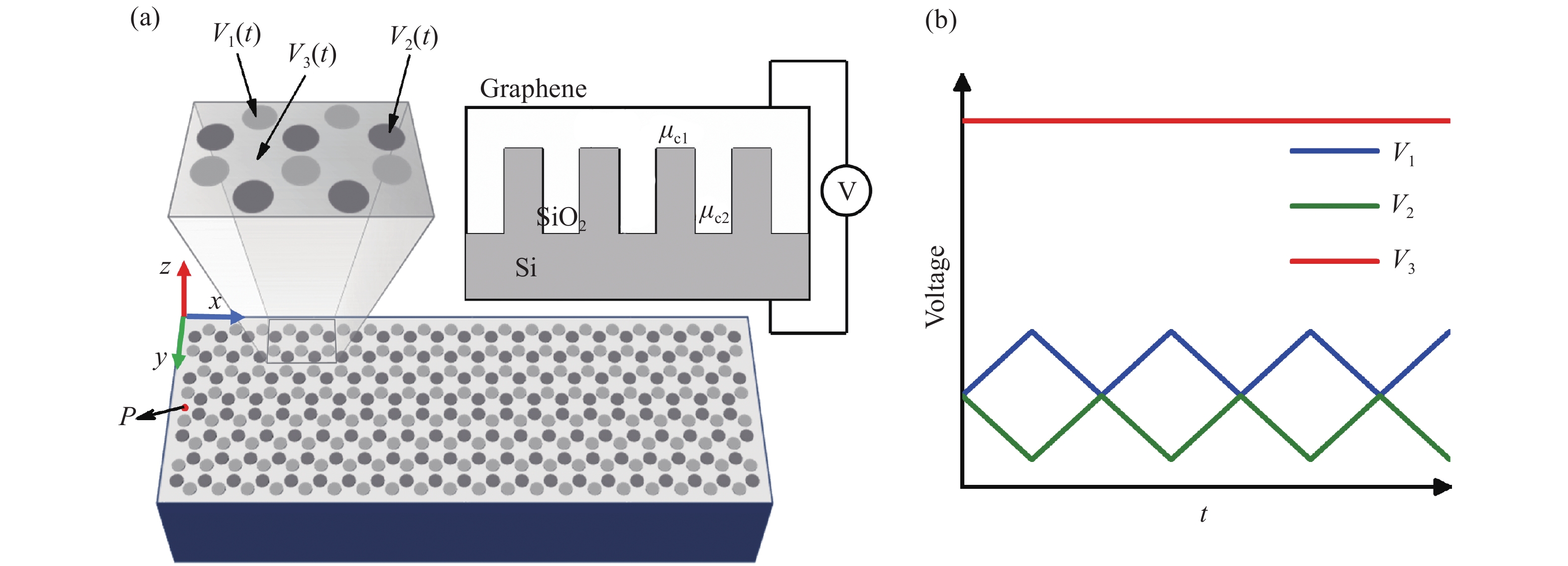
图 1 (a) 慢光波导的三维示意图,顶部是单层石墨烯纳米盘。石墨烯与空气接触,背景材料是 SiO2,衬底材料是Si。对不同的石墨烯纳米圆盘分别加载不同的偏置电压:V1(t),V2(t)和V3(t),右上图为电压的施加方式。(b) 石墨烯纳米盘外加偏置电压随时间周期性变化的曲线
Figure 1. (a) The three-dimensional schematic of slow light waveguide, with a single layer of graphene nanodisks at the top. The graphene is exposed to air on the top, the background material is SiO2, and the substrate material is Si. Different graphene nanodisks are applied with different bias voltages: V1(t), V2(t) and V3(t). The diagram on the right shows how voltage is applied. (b) The graphene nanodisk’s external bias voltage changes periodically with time
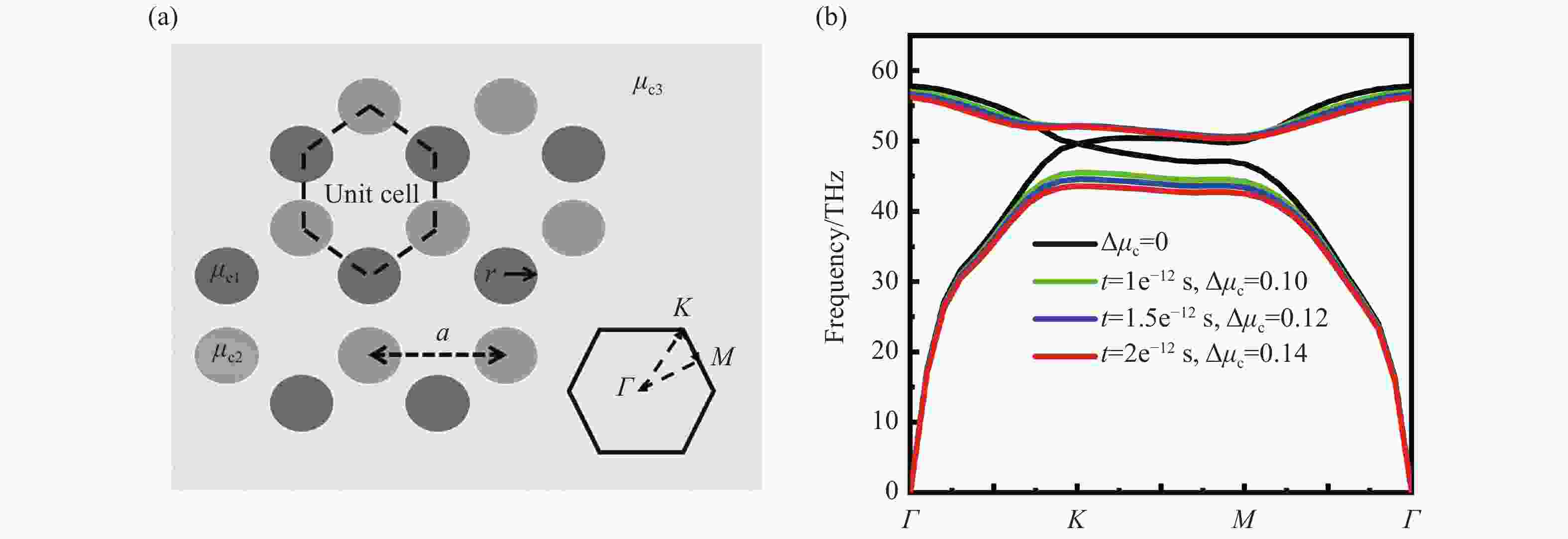
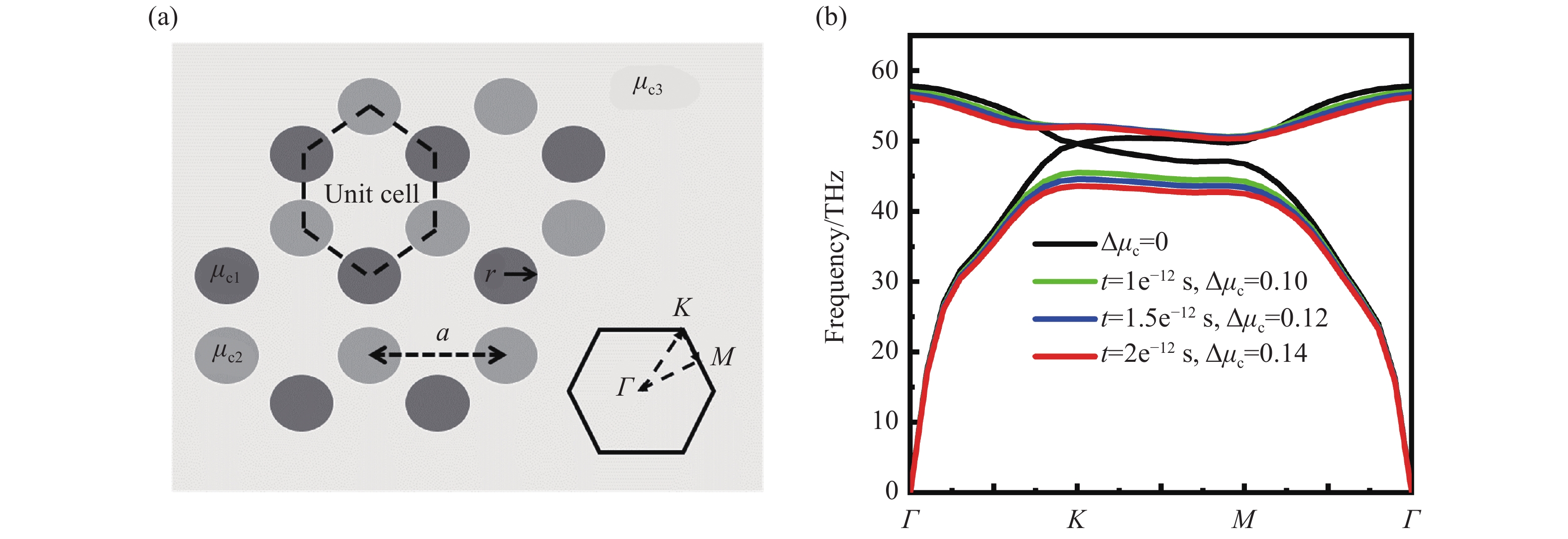
图 2 (a) 石墨烯等离激元时间晶体结构示意图。(b)在一个外加偏置电压变化周期内,石墨烯等离激元时间晶体在4个不同时刻的能带图
Figure 2. (a) Schematic diagram of graphene plasmon time crystal structure. (b) Energy band diagrams of graphene plasmon time crystals at four different moments in a cycle of external bias voltage change
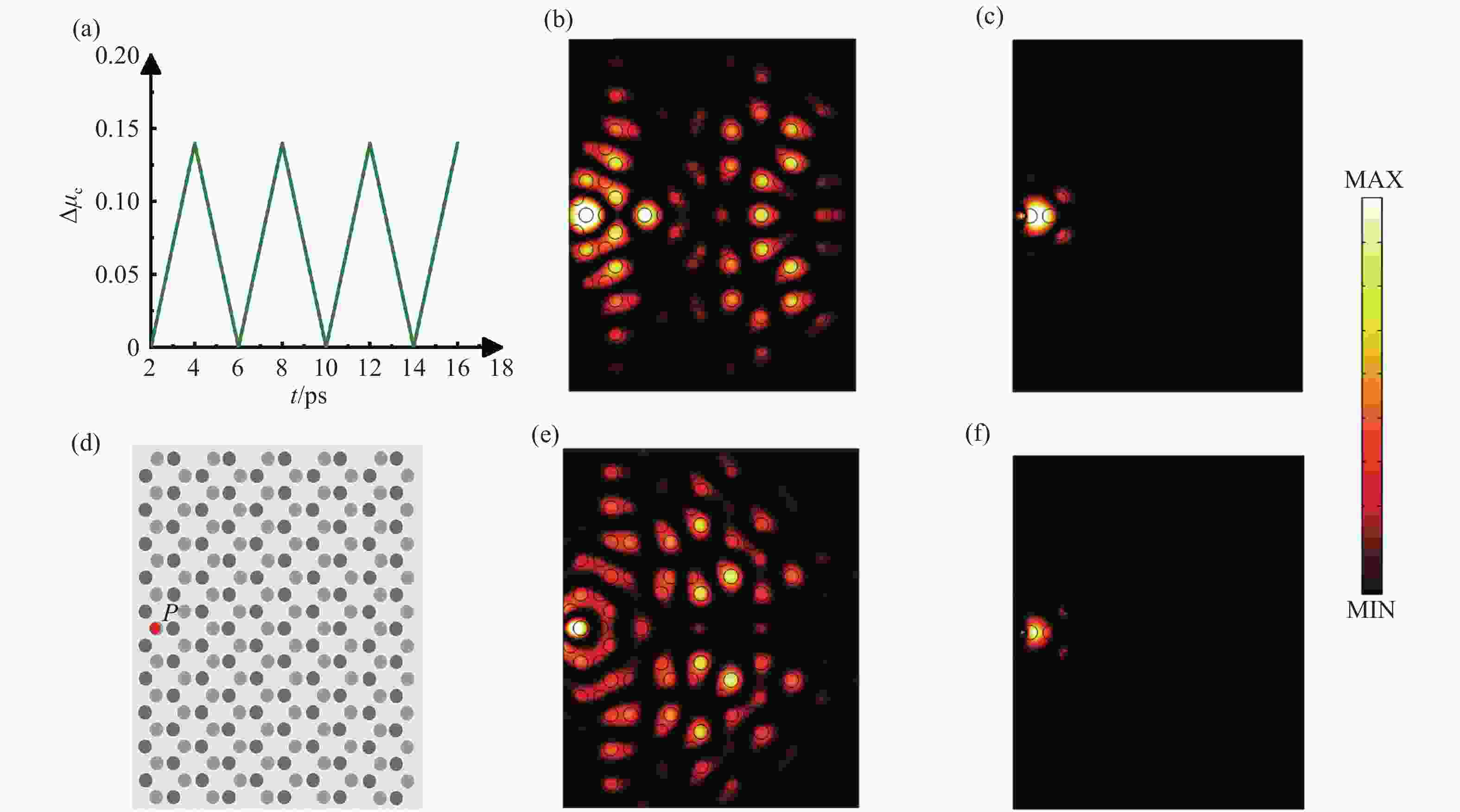
图 3 (a) 当
$ {\mu _{{\rm{c}}3}} $ =0.6 eV时,$ \Delta {\mu _{\rm{c}}} $ 与t的关系。(d) 5×10石墨烯等离激元时间晶体组成的一个区域,P是激发源的位置。(b),(c),(e)和(f)是传播过程中4个时刻的截图,时间节点分别是${t_{\rm{b}}} $ =3.20 e−12s,${t_{\rm{c}}} $ =4.16 e−12s,${t_{\rm{d}}} $ =5.82 e−12s和${t_{\rm{f}}} $ =8.24 e−12sFigure 3. (a) When μc3=0.6 eV, the relationship between ∆μc and t. (d) A region composed of 5×10 graphene plasmon time crystals. P is the position of the excitation source. (b), (c), (e) and (f) Screenshots of four moments in the propagation process at the time nodes of
${t_{\rm{b}}} $ =3.20 e−12s,${t_{\rm{c}}} $ =4.16 e−12s,${t_{\rm{d}}} $ =5.82 e−12s and${t_{\rm{f}}} $ =8.24 e−12s, respectively
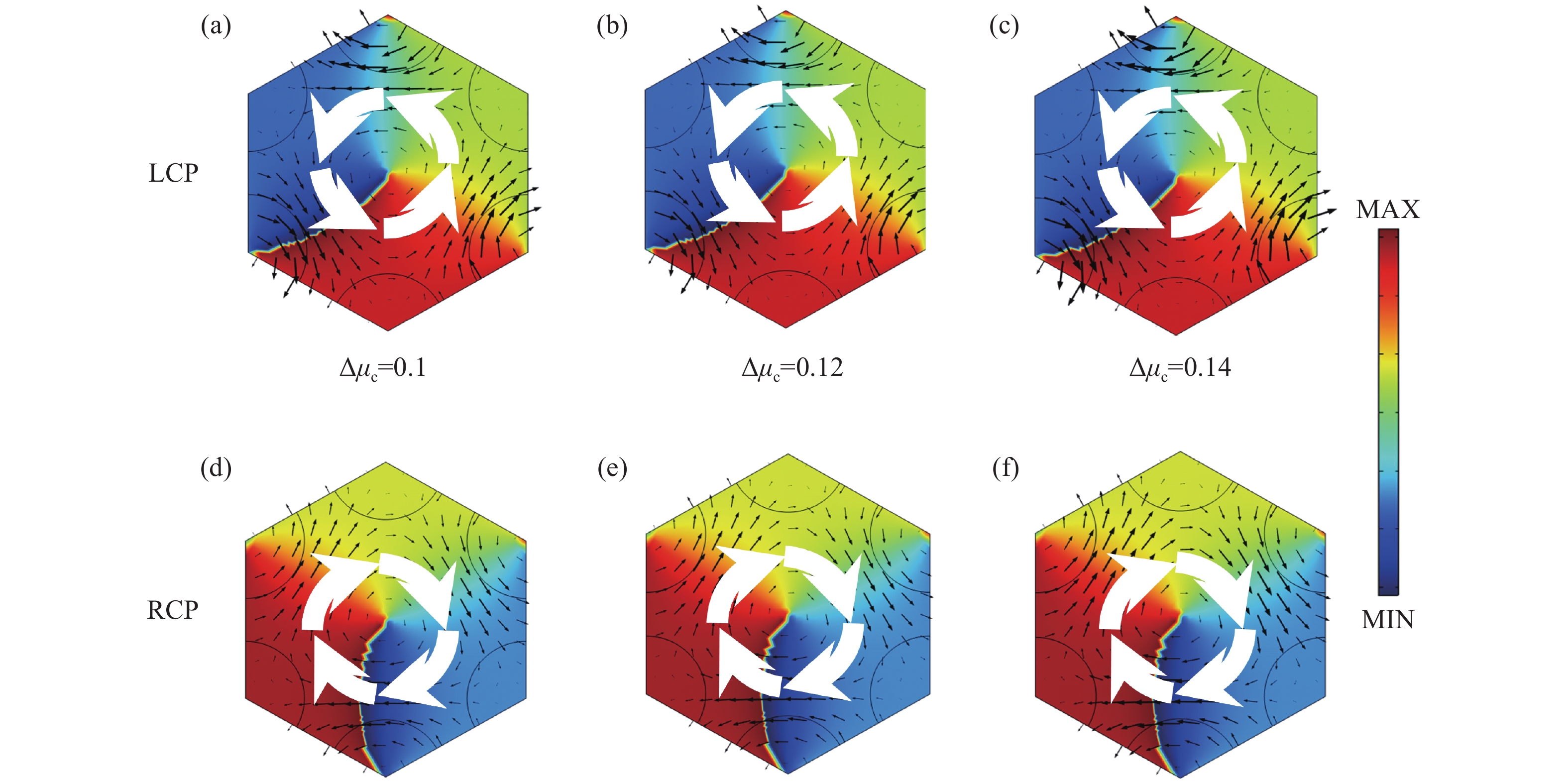
图 4 时间晶体在K点分别出现了左旋圆极化(LCP)和右旋圆极化(RCP)的相位分布,表示为电场在Z方向上的分量和面内坡印亭矢量(Px, Py)。(a)和(d)是在
$ \Delta {\mu _{\rm{c}}} $ =0.1 eV时刻,K点的相位分布图;(b)和(e)是在$ \Delta {\mu _{\rm{c}}} $ =0.12 eV时刻,K点的相位分布图;(c)和(f)在$ \Delta {\mu _{\rm{c}}} $ =0.14 eV时刻,K点的相位分布图Figure 4. The phase distributions of Left-handed Circularly Polarized (LCP) and Right-handed Circularly Polarized (RCP) of the time crystal appear at point K, which are expressed as the component of the electric field in the direction Z and the in-plane Poynting vector (Px, Py). (a) and (d) the phase distribution diagram of point K at the time of
$ \Delta {\mu _{\rm{c}}} $ =0.1 eV; (b) and (e) the phase distribution diagram of point K at the time of$ \Delta {\mu _{\rm{c}}} $ =0.12 eV; (c) and (f) the phase distribution diagram of point K at the time$ \Delta {\mu _{\rm{c}}} $ =0.14 eV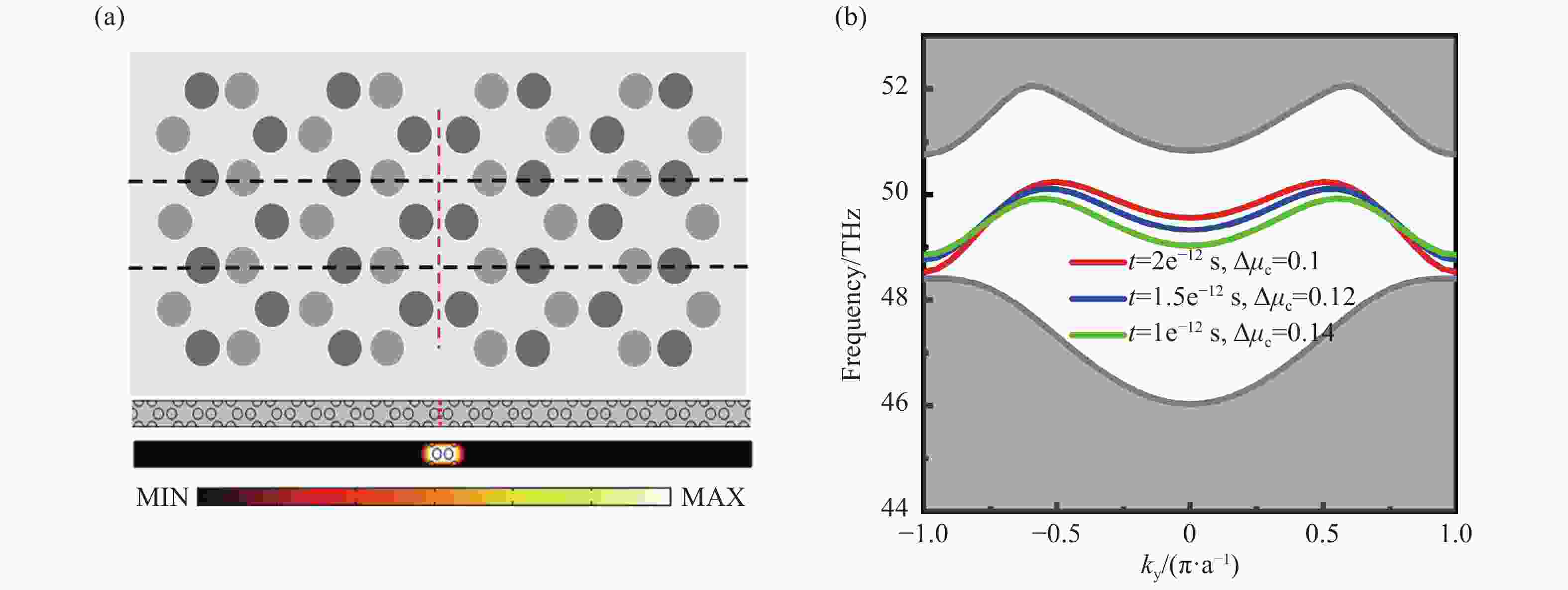
图 5 (a) 基于石墨烯等离激元时间晶体构成的Zigzag边界示意图。其中,底部分别是有限周期超胞单元的计算模型和仿真电场分布结果。(b)不同时刻下Zigzag边界模的色散曲线
Figure 5. (a) Schematic diagram of the Zigzag interface based on graphene plasmon time crystals, in which the bottom is the calculation model of the finite period super cell unit and the simulation electric field distribution results. (b) The dispersion curves of the Zigzag interface mode at different times
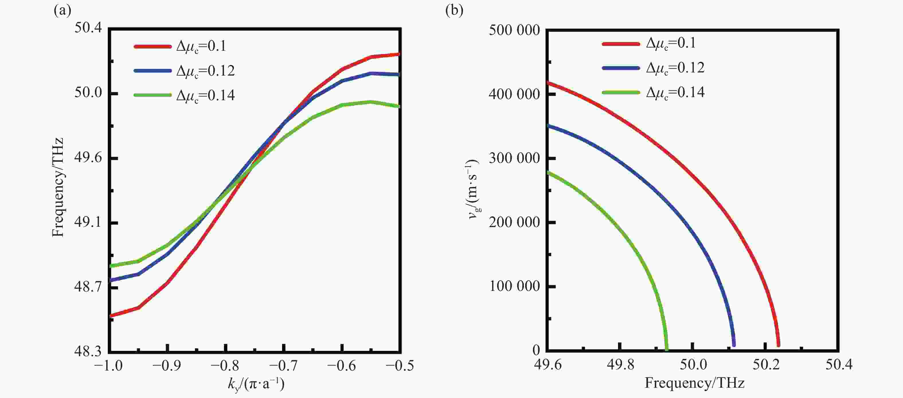
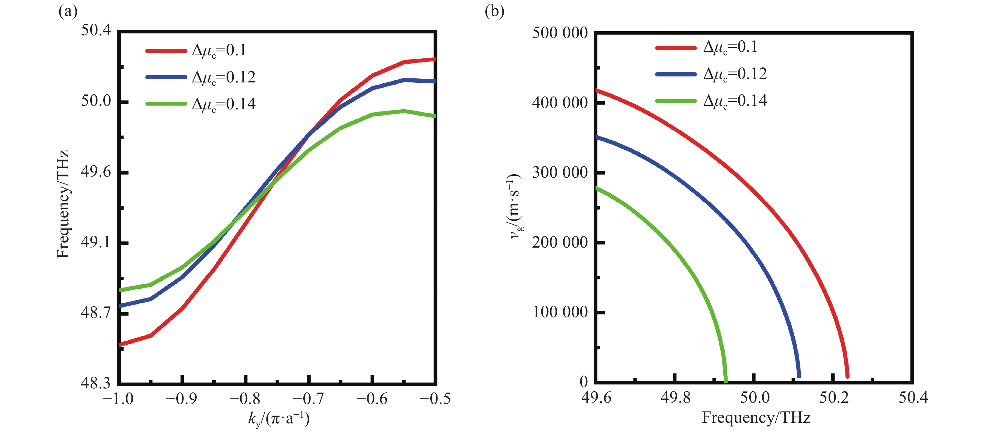
图 6 (a) 不同
$ \Delta {\mu _{\rm{c}}} $ 下拓扑边界所支持的边界模色散曲线。(b)不同$ \Delta {\mu _{\rm{c}}} $ 下群速度随频率的变化关系图Figure 6. (a) The boundary mode dispersion curve supported by the topological boundary under different
$ \Delta {\mu _{\rm{c}}} $ . (b) The relationship between group velocity and frequency under different$ \Delta {\mu _{\rm{c}}} $ 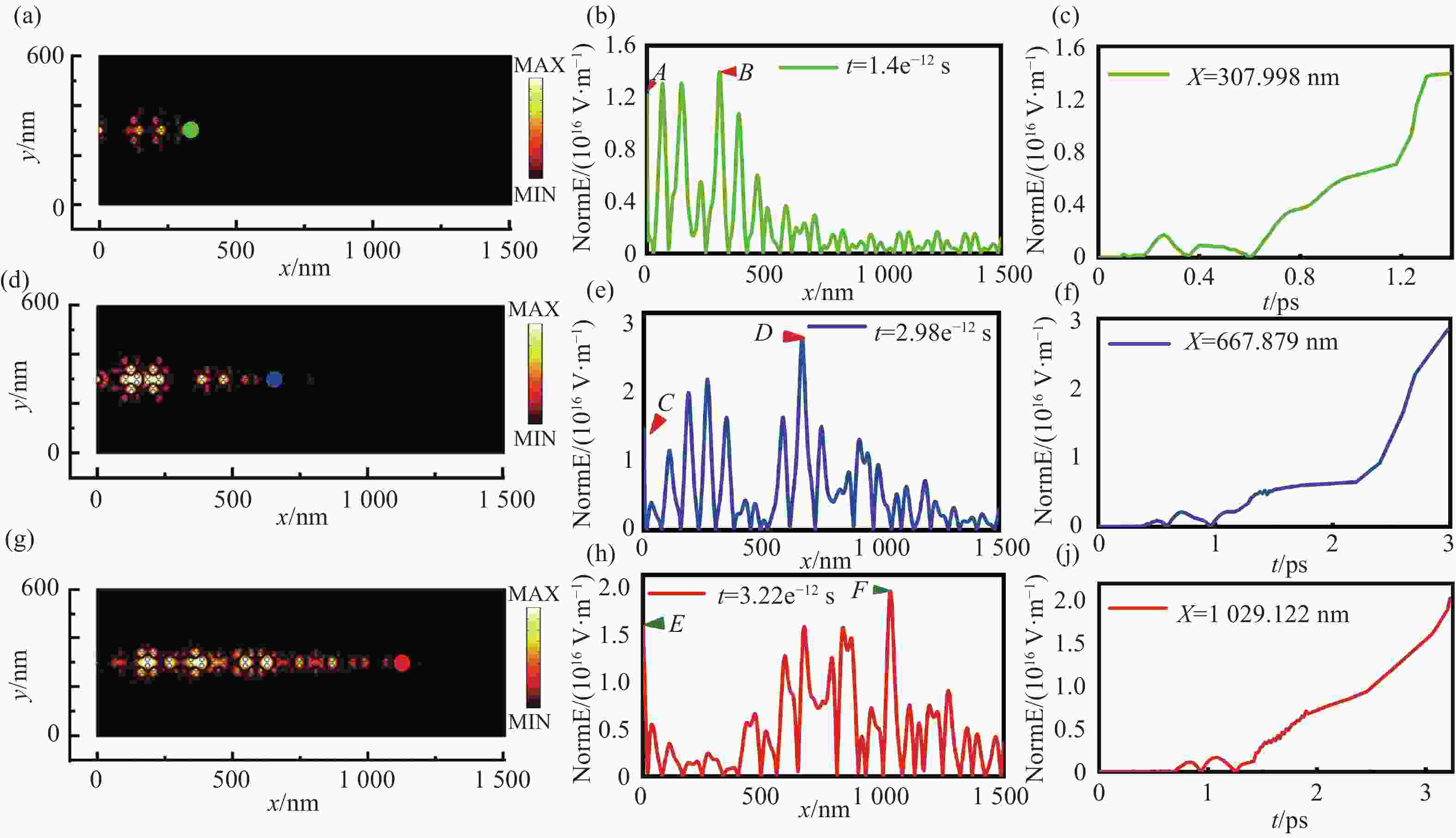
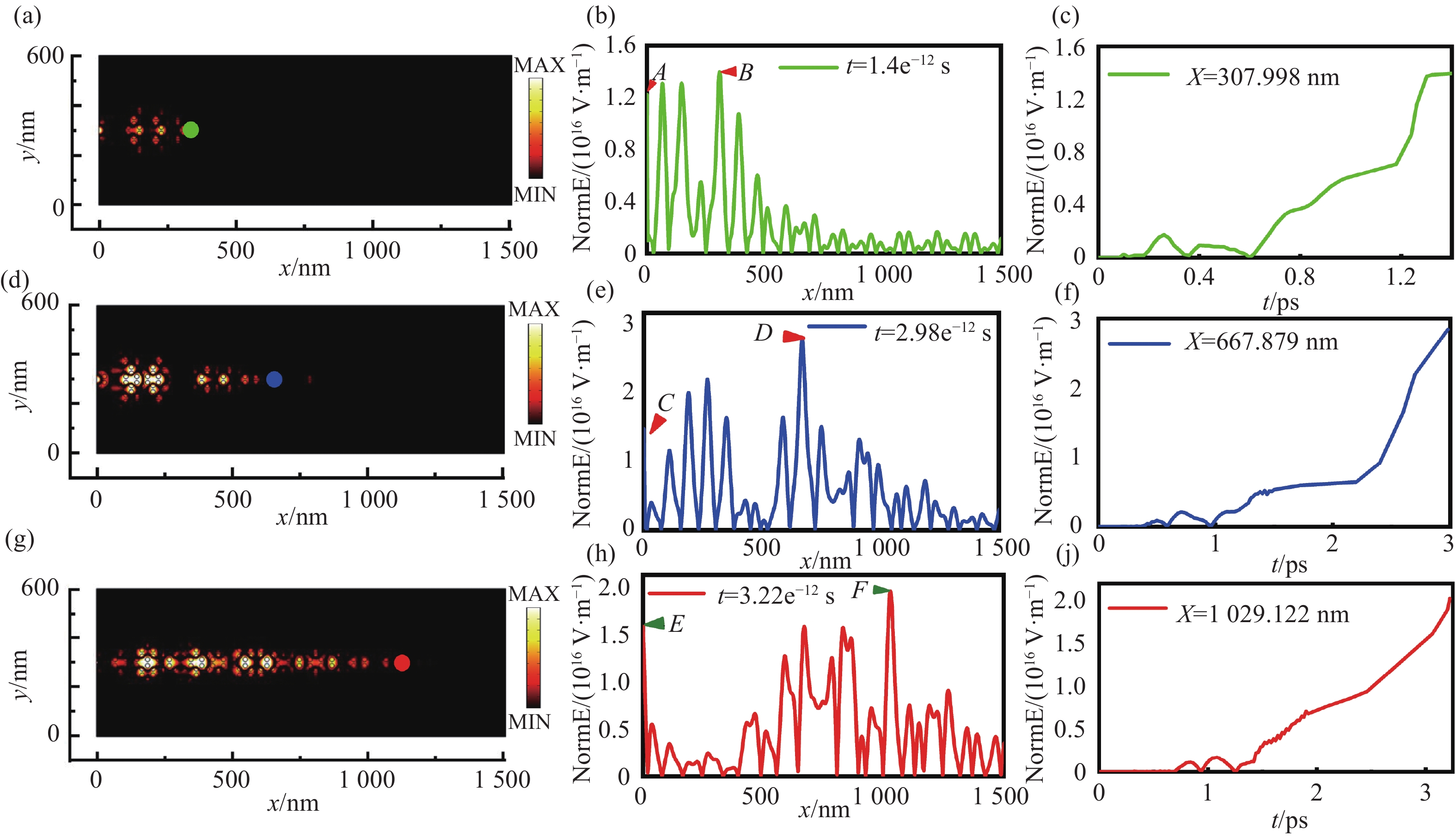
图 7 (a, d, g) t1,t2和t3时刻电场强度分布截图。(b, e, h) 不同t时刻Zigzag边界处截面电场图。(c, f, j) 光能捕获点处电场变化过程
Figure 7. (a, d, g) Screenshots of the electric field intensity distribution at t1, t2 and t3. (b, e, h) Cross-sectional electric field diagrams at the Zigzag boundary at different time t. (c, f, j) The changing process of the electric field at the capture point of light energy
-
[1] JIANG X P, CHEN D B, ZHANG ZH J, et al. Dual-channel optical switch, refractive index sensor and slow light device based on a graphene metasurface[J]. Optics Express, 2020, 28(23): 34079-34092. doi: 10.1364/OE.412442 [2] TORRIJOS-MORÁN L, GRIOL A, GARCÍA-RUPÉREZ J, et al. Slow light bimodal interferometry in one-dimensional photonic crystal waveguides[J]. Light:Science &Applications, 2021, 10(1): 16. [3] OSSIANDER M, HUANG Y W, CHEN W T, et al. Slow light nanocoatings for ultrashort pulse compression[J]. Nature Communications, 2021, 12(1): 6518. doi: 10.1038/s41467-021-26920-6 [4] YAN S Q, ZHU X L, FRANDSEN L H, et al. Slow-light-enhanced energy efficiency for graphene microheaters on silicon photonic crystal waveguides[J]. Nature Communications, 2017, 8: 14411. doi: 10.1038/ncomms14411 [5] ZHU K T, DENG T S, SUN Y, et al. Slow light property in ring-shape-hole slotted photonic crystal waveguide[J]. Optics Communications, 2013, 290: 87-91. doi: 10.1016/j.optcom.2012.10.055 [6] SCHEUER J. Optimal interfacing with coupled-cavities slow-light waveguides: mimicking periodic structures with a compact device[J]. Optics Express, 2017, 25(14): 16260-16273. doi: 10.1364/OE.25.016260 [7] CHEN H J. Multiple-Fano-resonance-induced fast and slow light in the hybrid nanomechanical-resonator system[J]. Physical Review A, 2021, 104(1): 013708. doi: 10.1103/PhysRevA.104.013708 [8] NOTOMI M, YAMADA K, SHINYA A, et al. Extremely large group-velocity dispersion of line-defect waveguides in photonic crystal slabs[J]. Physical Review Letters, 2001, 87(25): 253902. doi: 10.1103/PhysRevLett.87.253902 [9] ITO H, KUSUNOKI Y, MAEDA J, et al. Wide beam steering by slow-light waveguide gratings and a prism lens[J]. Optica, 2020, 7(1): 47-52. doi: 10.1364/OPTICA.381484 [10] DONG J W, CHEN X D, ZHU H Y, et al. Valley photonic crystals for control of spin and topology[J]. Nature Materials, 2017, 16(3): 298-302. doi: 10.1038/nmat4807 [11] YOSHIMI H, YAMAGUCHI T, OTA Y, et al. Slow light waveguides in topological valley photonic crystals[J]. Optics Letters, 2020, 45(9): 2648-2651. doi: 10.1364/OL.391764 [12] KHANIKAEV A B, SHVETS G. Two-dimensional topological photonics[J]. Nature Photonics, 2017, 11(12): 763-773. doi: 10.1038/s41566-017-0048-5 [13] LUSTIG E, SHARABI Y, SEGEV M. Topological aspects of photonic time crystals[J]. Optica, 2018, 5(11): 1390-1395. doi: 10.1364/OPTICA.5.001390 [14] WANG N, ZHANG ZH Q, CHAN C T. Photonic Floquet media with a complex time-periodic permittivity[J]. Physical Review B, 2018, 98(8): 085142. doi: 10.1103/PhysRevB.98.085142 [15] GIERGIEL K, DAUPHIN A, LEWENSTEIN M, et al. Topological time crystals[J]. New Journal of Physics, 2019, 21(5): 052003. doi: 10.1088/1367-2630/ab1e5f [16] GANGARAJ S A H, MONTICONE F. Topological waveguiding near an exceptional point: defect-immune, slow-light, and loss-immune propagation[J]. Physical Review Letters, 2018, 121(9): 093901. doi: 10.1103/PhysRevLett.121.093901 [17] JIN D F, CHRISTENSEN T, SOLJAČIĆ M, et al. Infrared topological plasmons in graphene[J]. Physical Review Letters, 2017, 118(24): 245301. doi: 10.1103/PhysRevLett.118.245301 [18] WANG Y P, YOU J W, LAN ZH H, et al. Topological valley plasmon transport in bilayer graphene metasurfaces for sensing applications[J]. Optics Letters, 2020, 45(11): 3151-3154. doi: 10.1364/OL.393302 [19] GUO X, WU X, CUI H, et al. Slow light performance enhancement of graphene-based photonic crystal waveguide[J]. Physics Letters A, 2019, 383(16): 1983-1987. doi: 10.1016/j.physleta.2019.03.032 [20] XIONG L, FORSYTHE C, JUNG M, et al. Photonic crystal for graphene plasmons[J]. Nature Communications, 2019, 10(1): 4780. doi: 10.1038/s41467-019-12778-2 [21] WU X X, YAN M, TIAN J X, et al. Direct observation of valley-polarized topological edge states in designer surface plasmon crystals[J]. Nature Communications, 2017, 8(1): 1304. doi: 10.1038/s41467-017-01515-2 [22] YOU J W, LAN ZH H, BAO Q L, et al. Valley-Hall topological plasmons in a graphene nanohole plasmonic crystal waveguide[J]. IEEE Journal of Selected Topics in Quantum Electronics, 2020, 26(6): 4600308. [23] HAO Y, KONG M, LU J. Control of light speed in single-ring microresonators with gain[J]. Chinese Optics, 2009, 2(6): 482-488. (in Chinese) doi: 10.3969/j.issn.2095-1531.2009.06.003 [24] CAO T, FANG L H, CAO Y, et al. Dynamically reconfigurable topological edge state in phase change photonic crystals[J]. Science Bulletin, 2019, 64(12): 814-822. doi: 10.1016/j.scib.2019.02.017 [25] HONG W, WANG L Q, LIN J P. Research progress of polymeric hierarchical microstructures and their properties[J]. Chinese Journal of Applied Chemistry, 2021, 38(10): 1310-1325. (in Chinese) [26] ZHUANG S N, CHEN J F, LIANG W Y, et al. Zero GVD slow-light originating from a strong coupling of one-way modes in double-channel magneto-optical photonic crystal waveguides[J]. Optics Express, 2021, 29(2): 2478-2487. doi: 10.1364/OE.412460 [27] ZURITA-SÁNCHEZ J R, HALEVI P, CERVANTES-GONZÁLEZ J C. Reflection and transmission of a wave incident on a slab with a time-periodic dielectric function ϵ (t)[J]. Physical Review A, 2009, 79(5): 053821. doi: 10.1103/PhysRevA.79.053821 [28] CAO T, LIU K, LI Y, et al. Tunable optical metamaterials and their applications[J]. Chinese Optics, 2021, 14(4): 968-985. (in Chinese) doi: 10.37188/CO.2021-0080 [29] FAN ZH, ZHANG SH SH, TANG J H, et al. Structure, preparation and application of graded nanomaterials[J]. Chinese Journal of Applied Chemistry, 2020, 37(5): 489-501. (in Chinese) doi: 10.11944/j.issn.1000-0518.2020.05.190248 [30] MA J, WANG ZH G. Band structure and topological phase transition of photonic time crystals[J]. Optics Express, 2019, 27(9): 12914-12922. doi: 10.1364/OE.27.012914 [31] SHARABI Y, LUSTIG E, SEGEV M. Disordered photonic time crystals[J]. Physical Review Letters, 2021, 126(16): 163902. doi: 10.1103/PhysRevLett.126.163902 [32] CHENG Q Q, PAN Y M, WANG H Q, et al. Observation of anomalous π mode in photonic floquet engingeering[J]. Physical Review Letters, 2019, 12: 173901. doi: 10.1103/PhysRevLett.122.173901 [33] ZENG L W, XU J, WANG CH E, et al. Photonic time crystals[J]. Scientific Reports, 2017, 7(1): 17165. doi: 10.1038/s41598-017-17354-6 [34] PAN Y M, WANG B. Time-crystalline phases and period-doubling oscillations in one-dimensional Floquet topological insulators[J]. Physical Review Research, 2020, 2(4): 043239. doi: 10.1103/PhysRevResearch.2.043239 [35] LIU H, WANG H N, XIE B Y, et al. Progress of two-dimensional photonic topological insulators[J]. Chinese Optics, 2021, 14(4): 935-954. (in Chinese) doi: 10.37188/CO.2021-0076 [36] FENG L, ZHU X F,YANG S, et al. Deomonstration of a large-scale optical exceptional point structure[J]. Optics Express, 2014, 22(2): 1760. doi: 10.1364/OE.22.001760 [37] RAZA S, BOZHEVOLNYI S I. Slow-light plasmonic metamaterial based on dressed-state analog of electromagnetically induced transparency[J]. Optics Letters, 2015, 40(18): 4253-4256. doi: 10.1364/OL.40.004253 [38] ABOOD I, ELSHAHAT S, OUYANG ZH B. High figure of merit optical buffering in coupled-slot slab photonic crystal waveguide with ionic liquid[J]. Nanomaterials, 2020, 10(9): 1742. doi: 10.3390/nano10091742 -

 下载:
下载:


计量
- 文章访问数: 866
- HTML全文浏览量: 623
- PDF下载量: 164
- 被引次数: 0
