


Recent progress on synthesis and optical characterization of two-dimensional Bi2O2Se
-
摘要:
二维(2D)半导体材料Bi2O2Se由于具有独特的晶体结构与能带结构、超高的载流子迁移率和优异的稳定性,在紫外-可见-近红外光谱区的高性能电子与光电应用领域有着广阔的前景。本文综述了Bi2O2Se的材料制备与光学表征最新研究进展:首先,介绍了2D Bi2O2Se的制备方法及生长机理,包括化学气相沉积法(CVD)、湿化学工艺、分子束外延法(MBE)和脉冲激光沉积法(PLD)等;其次,介绍了其晶体结构和电子能带结构的基本性质;接下来,通过稳态光谱的研究,可以对2D Bi2O2Se随厚度变化的带隙等物理性质进行研究;通过研究其晶体振动模式,可进一步研究2D Bi2O2Se材料的缺陷形态、温度系数与热导率;此外,超快光谱技术也可以帮助研究2D Bi2O2Se材料内部载流子的弛豫过程与输运性能;最后,简述了当前Bi2O2Se研究面临的挑战与应用的前景。
Abstract:Two-dimensional (2D) Bi2O2Se has attracted broad attention in the field of electronic and optoelectronic applications in the UV-Vis-NIR region due to its unique crystal structure, energy band, high carrier mobility, and excellent stability. In this paper, we review the recent research progress in the material synthesis and optical characterization of Bi2O2Se. Firstly, the synthetic method and growth mechanism of 2D Bi2O2Se are introduced, including Chemical Vapor Deposition (CVD), wet chemical process, Molecular Beam Epitaxy (MBE) and Pulsed Laser Deposition (PLD), etc. Via steady-state spectrum study, the properties change of 2D Bi2O2Se with thickness change can be studied, such as the band gap. The defect type, temperature coefficient and thermal conductivity of 2D Bi2O2Se material can be further studied by focusing on the crystal vibration mode. Transient spectrum techniques can benefit the study of relaxation process and carriers transport properties in 2D Bi2O2Se materials. Finally, we summarize the existing challenges and application prospects for the promising Bi2O2Se field.
-

图 1 Bi2O2Se的CVD制备方法及其原理[31-33, 67-68]。(a) CVD生长原理图[31-32]; (b) 550 °C下生长30分钟的Bi2O2Se纳米片的光学图像;(c) 合成的2D Bi2O2Se晶体的平均畴尺寸与生长温度的函数关系[32]; (d) c-MOCVD的生长原理图;(e) 通过原子分辨率ABF-STEM(左)和HAADFSTEM(右)观察到的Bi2O2Se 在[100]方向(Bi2O2Se的z轴方向)的晶体结构图[67];(f) RF CVD生长原理图[33];(g) 样品的平均尺寸与RF保持时间之间的关系。其中虚线为拟合曲线
Figure 1. CVD synthesis method and mechanism of Bi2O2Se[31-33, 67-68]. (a) Schematic of CVD growth[31-32]. Copyright © 2021, AIP Publishing. (b) Optical image of Bi2O2Se nanosheets grown at 550 °C for 30 min. (c) Average domain size of synthesized 2D Bi2O2Se crystals as a function of growth temperature. Copyright © 2017, American Chemical Society[32]. (d) Schematic of the c-MOCVD growth. (e) Crystal structure of Bi2O2Se in the [100] direction (the z-axis direction of Bi2O2Se) observed by atomic-resolution ABF-STEM (left) and HAADFSTEM (right). Copyright © 2021 American Chemical Society[67]. (f) Schematic of the RF CVD growth[33]. (g) The relationship between the average size of the samples and the RF holding time. The dotted line is the fitted curve. Copyright © 2021, American Chemical Society

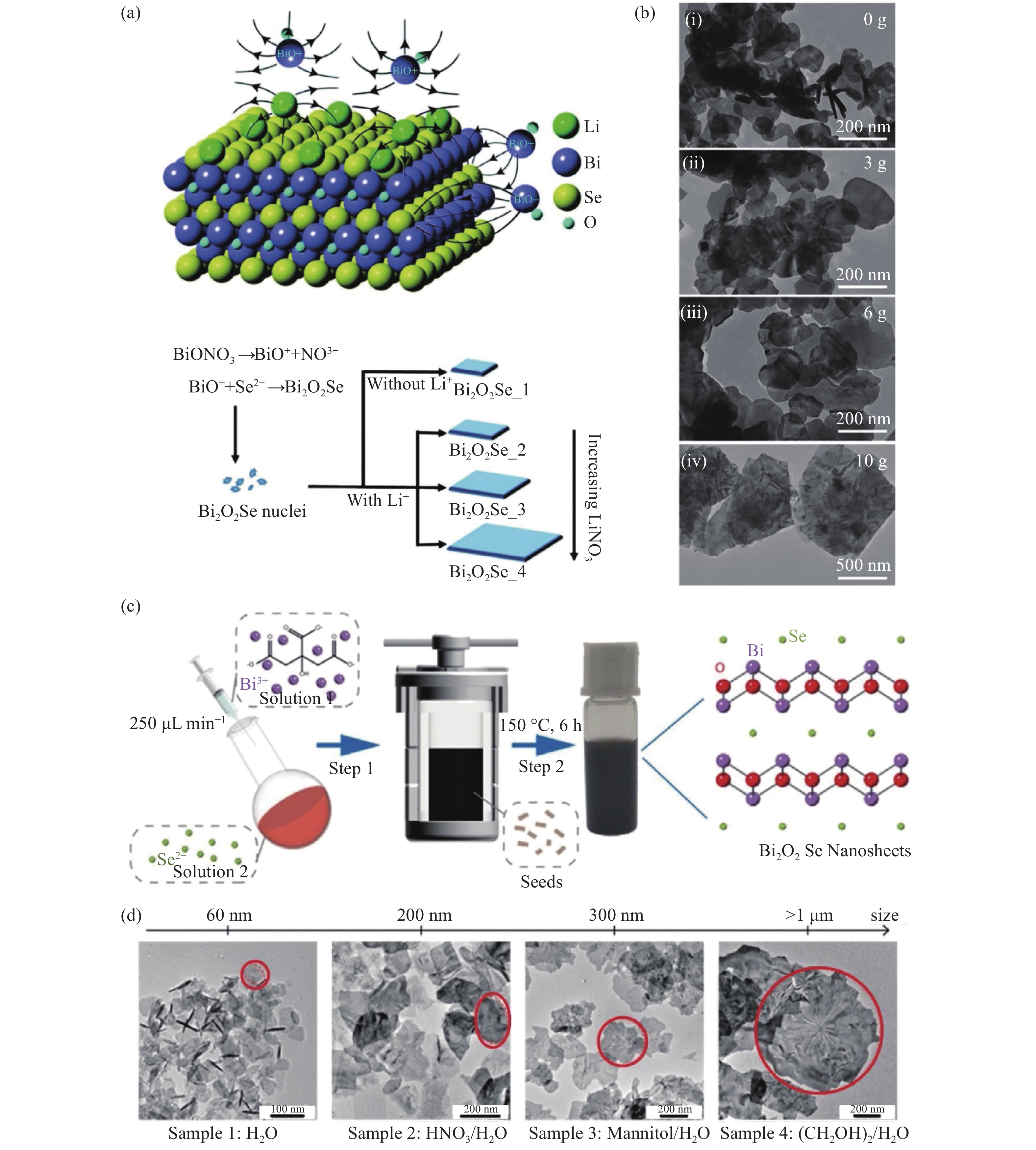
图 2 Bi2O2Se的湿化学工艺制备方法[34-35]。(a) 超薄Bi2O2Se纳米片在LiNO3溶液下的生长机理;(b) 在不同LiNO3的质量(ⅰ–0g,ⅱ–3g,ⅲ–6g,ⅳ–10g)下获得的Bi2O2Se纳米片的形貌图,(c) 两步合成Bi2O2Se纳米片的工艺示意图;(d) 通过调整溶液1中溶剂类型(样品1—去离子水,样品2—HNO3溶液,样品3—甘露醇溶液,样品4—乙二醇和去离子水的混合物)获得的Bi2O2Se纳米片的形貌图
Figure 2. Fabrication of Bi2O2Se by wet-chemical process[34-35]. (a) Growth mechanism of ultrathin Bi2O2Se nanosheets in LiNO3 solution. (b) Morphology of Bi2O2Se nanosheets obtained with different LiNO3 masses (ⅰ–0g, ⅱ–3g, ⅲ–6g, ⅳ–10g). Copyright © 2020, Royal Society of Chemistry. (c) Schematic of the two-step synthesis of Bi2O2Se nanosheets. (d) The morphology of Bi2O2Se nanosheets obtained by adjusting the solvent types in solution 1 (sample 1—water, sample 2—HNO3 solution, sample 3—mannitol solution, sample 4—ethylene glycol and water mixture). Copyright © 2021, Elsevier
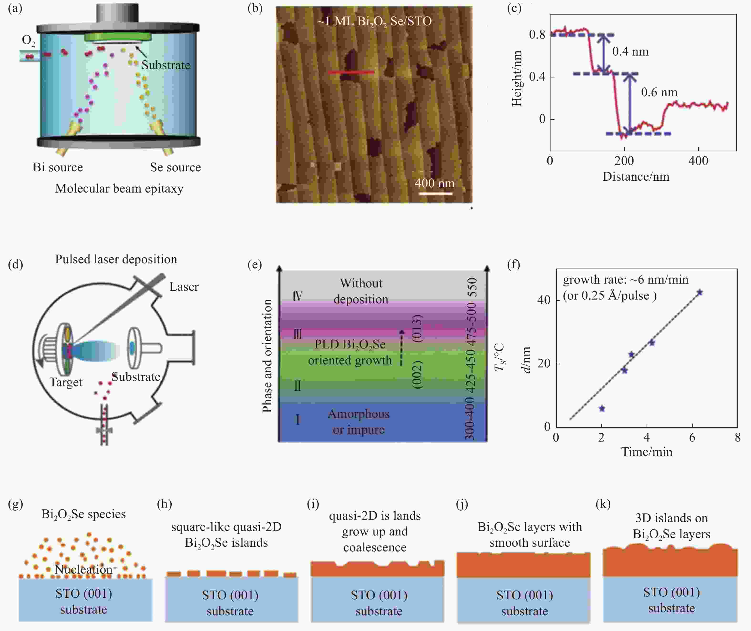
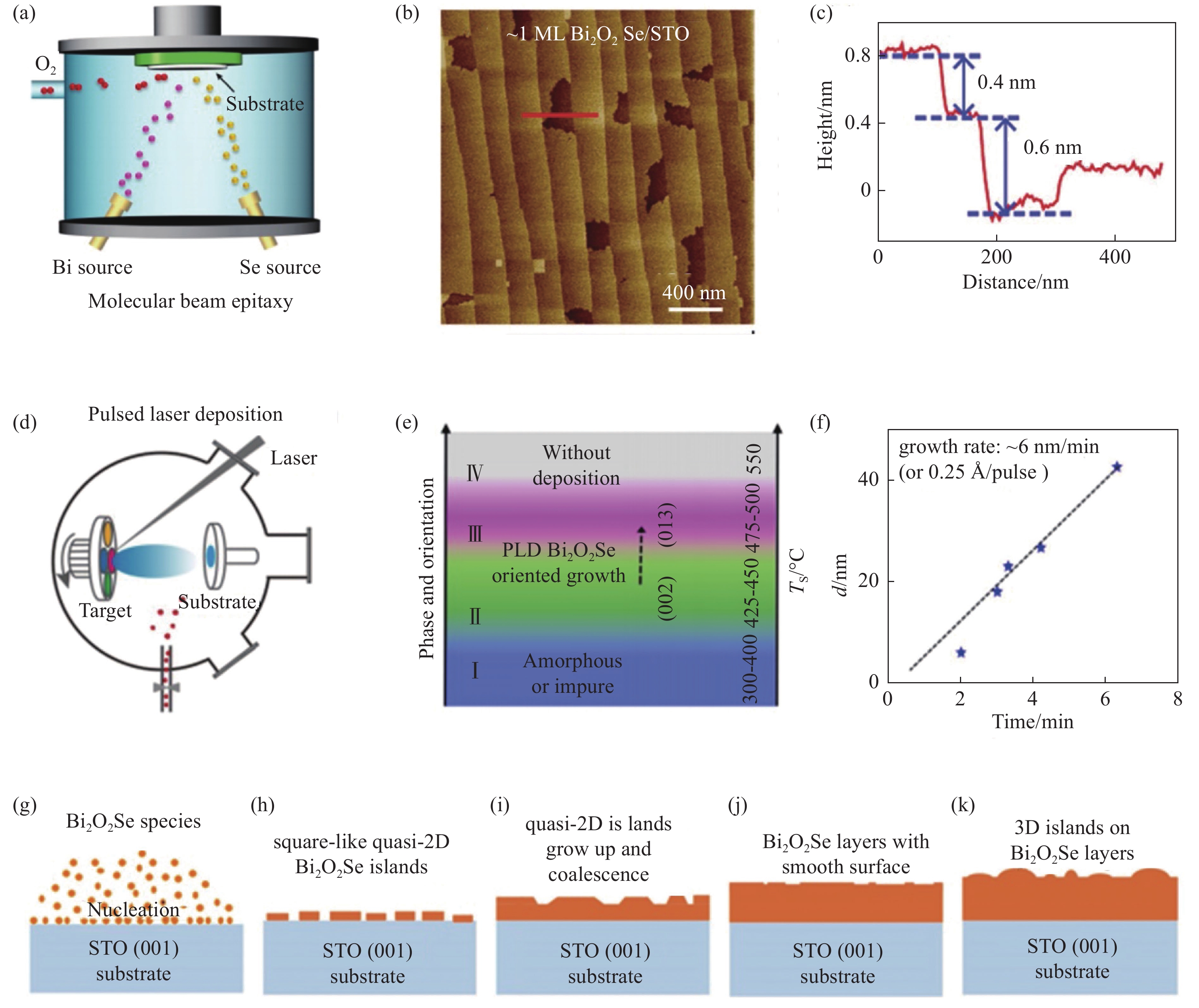
图 3 (a) MBE制备Bi2O2Se原理图。Bi源和Se源在稀释的氧气气氛中共蒸发。(b) 单层Bi2O2Se纳米片AFM形貌图。(c) 单层Bi2O2Se纳米片的AFM的厚度测量结果图。(d) PLD方法制备原理图。(e) 通过PLD技术在STO衬底上生长的Bi2O2Se薄膜的衬底温度Ts、相关相位和面外取向图。(f) Bi2O2Se膜厚与沉积持续时间的依赖关系。(g-k) 通过PLD技术在STO衬底上生长Bi2O2Se薄膜的过程示意图[37, 38, 73, 74]
Figure 3. (a) MBE fabrication and mechanism of Bi2O2Se. Bi source and Se source co-evaporated in the dilute oxygen atmosphere. Copyright © 2021, American Chemical Society. (b) AFM image of single-layer Bi2O2Se nanosheet. (c) AFM image for thickness measurement results of single-layer Bi2O2Se nanosheet. Copyright © 2019, John Wiley and Sons. (d) Schematic of PLD method preparation. Copyright © 2021, AIP Publishing. (e) A diagram of the substrate temperature Ts dependent phase and out-of-plane orientation for PLD-grown Bi2O2Se films on STO. (f) Dependence of Bi2O2Se film thickness on deposition duration. (g-k) Schematic of Bi2O2Se films grown on STO substrates by PLD method. Copyright © 2021, IOP Publishing[37, 38, 73, 74]
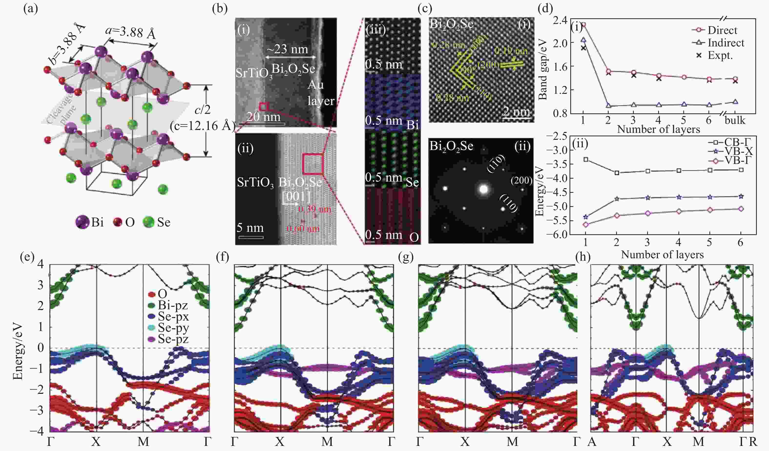
图 4 (a) Bi2O2Se的四方晶体结构,由交替的
$\left[ {{\rm{Bi}}_2{{\rm{O}}_2}} \right]_n^{2n + }$ 层和$\left[ {{\rm{Se}}_2} \right]_n^{2n - }$ 层组成。(b) 在Ts = 425 °C下沉积的Bi2O2Se/STO纳米片的横截面低倍和高倍分辨透射电镜图。(c) Bi2O2Se的HRTEM图像和SAED图。(d) (i) 计算得到的带隙与超薄Bi2O2Se纳米片层数的函数关系。直接带隙(圆形)、间接带隙(三角形)和实验光学带隙(十字)。(ii) VB-Γ(菱形)和VB-X(五角星)处最高价带以及CB-Γ(正方形)处最低导带的能级。(e) 单层、(f) 双层、(g) 三层、(h) 块体Bi2O2Se的能带结构。VBM设置为0 eV,由水平虚线标记。[25, 38-39, 77]Figure 4. (a) Body-center tetragonal crystal structure of Bi2O2Se, consisting of alternating Bi2O2 and Se layers. (b) Cross-section examination of the Bi2O2Se/STO film deposited at Ts = 425 °C by low-magnification TEM and HAADF-STEM characterizations. Copyright © 2020, IOP Publishing. (c) HRTEM image and SAED image of Bi2O2Se. Copyright © 2021, John Wiley and Sons. (d) (i) Calculated band gaps as a function of the number of layers for ultrathin Bi2O2Se films. Direct band gap (Γ-Γ) (circles) and indirect band gap (X-Γ) (triangles) and experimental optical band gap (Expt.) (Crosses). (ii) Energy of band edge with respect to the vacuum level for the highest valence band at VB-Γ (Diamonds) and at VB-X (Stars), and lowest conduction band at CB-Γ (Squares). Orbital-projected band structures for (e) monolayer, (f) bilayer, (g) tri-layer, (h) bulk Bi2O2Se. Band weights of Bi 6p, Se 4p and O 2p orbitals are sized by symbols. Valence band maximum (VBM) is set as 0 eV, as marked by the horizontal dashed lines. Copyright © 2021, Elsevier.[25, 38-39, 77]

图 5 Bi2O2Se的光学特性图[31, 40, 85]。(a) CVD生长的原子薄Bi2O2Se晶体的光学显微镜(OM)图像,具有反射率模式(顶部)和透射率模式(底部),云母上具有不同的层数(从1到6L);(b) 对(a)中具有不同层数的Bi2O2Se纳米片进行微光学测量。(c) Bi2-xCexO2Se (0 ≤ x ≤ 0.15)的UV-Vis-NIR漫反射光谱;(d) 云母上不同厚度的Bi2O2Se (编号1到7);(e) 对(d)中不同厚度的Bi2O2Se 纳米片的光学对比度的测量;(f) 对(e)中取550 nm处的对比度值与厚度之间的关系
Figure 5. Optical properties of Bi2O2Se[31, 40, 85]. (a) OM images of CVD-grown atomically thin Bi2O2Se crystals with different number of layers (from 1L to 6L) on mica with the reflectance mode (top) and transmittance mode (bottom). (b) Micro-optical measurements for Bi2O2Se nanosheets with different various layers in (a). Copyright © 2017, American Chemical Society. (c) UV-Vis-NIR diffuse reflectance spectra of Bi2-xCexO2Se (0 ≤ x ≤ 0.15). Copyright © 2021, Elsevier. (d) Bi2O2Se of different thickness on mica (from 1 to 7). (e) Measurement of the optical contrast of Bi2O2Se nanosheets with different thicknesses in (d). (f) The relationship between the contrast value and thickness at 550 nm in (e)
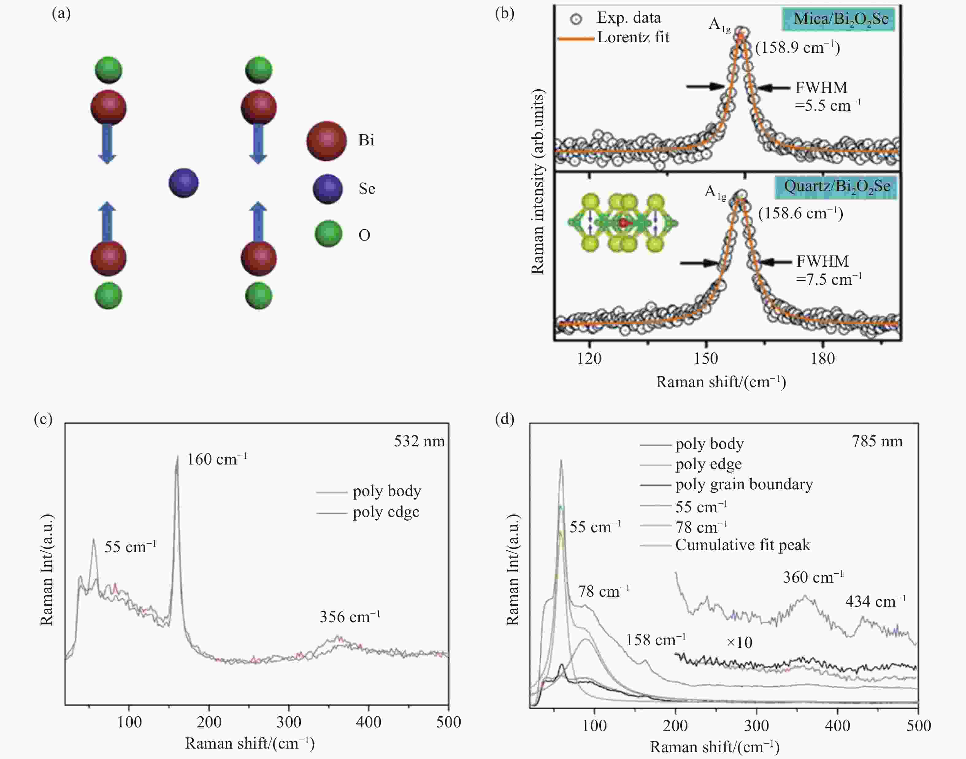
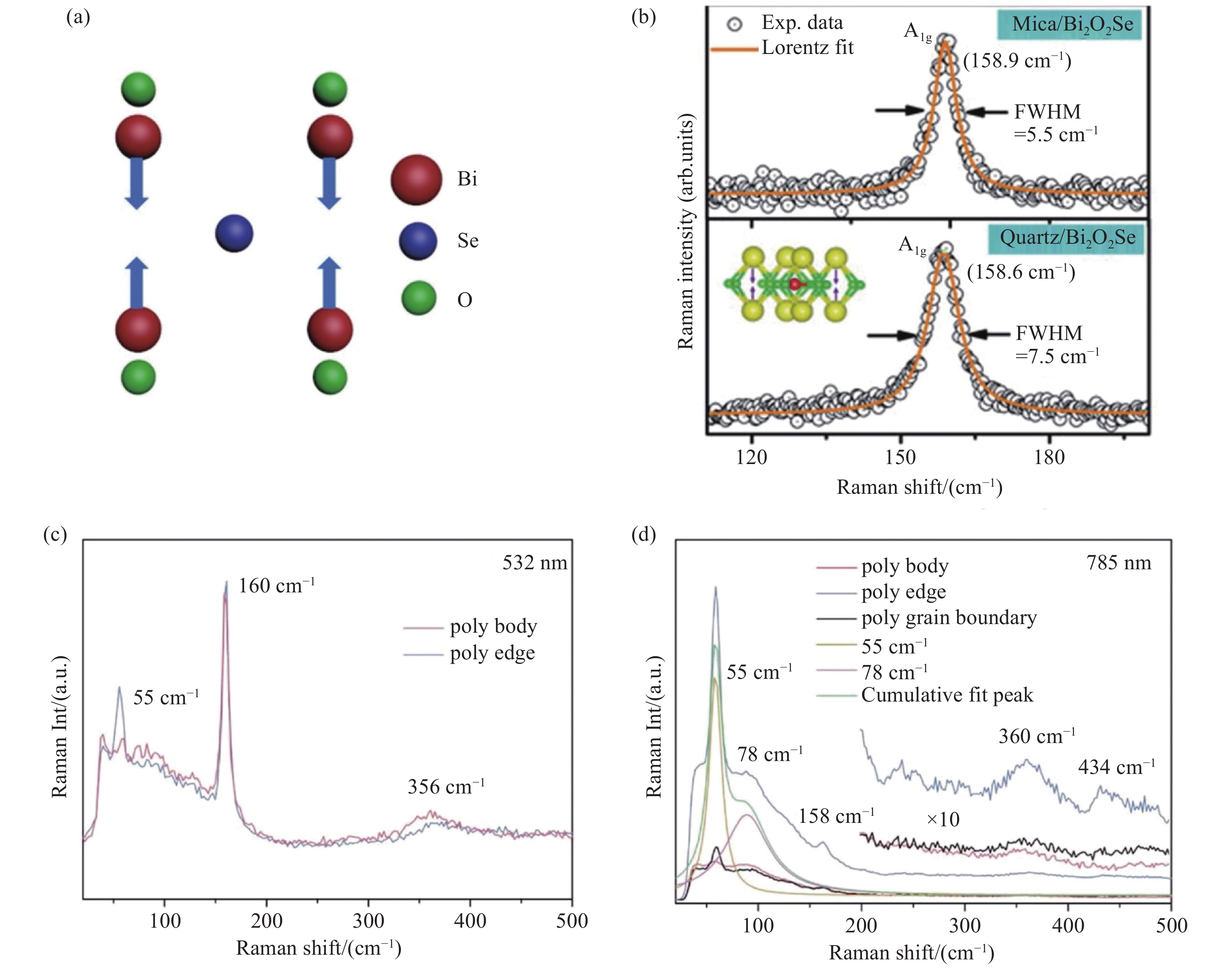
图 6 Bi2O2Se纳米片的拉曼光谱[32, 41, 43]。(a) Bi2O2Se的A1g振动模式;(b) Bi2O2Se纳米片在不同衬底的拉曼光谱[41];Bi2O2Se纳米片在 (c) 532 nm和(d)785 nm激光激发时产生的拉曼光谱[43]
Figure 6. Raman spectrum of Bi2O2Se flake[32, 41, 43]. (a) The A1g vibration mode of Bi2O2Se. Copyright © 2019, AIP Publishing. (b) Raman spectra of Bi2O2Se flakes grown on quartz and mica substrates showing the characteristic A1g Raman mode. Copyright © 2021, AIP Publishing. (c)~(d) Individual Raman spectra of the center and edges of the polygons: (c) 532 nm excitation mode. (d) 785 nm excitation mode. Copyright © 2022, American Chemical Society[43]
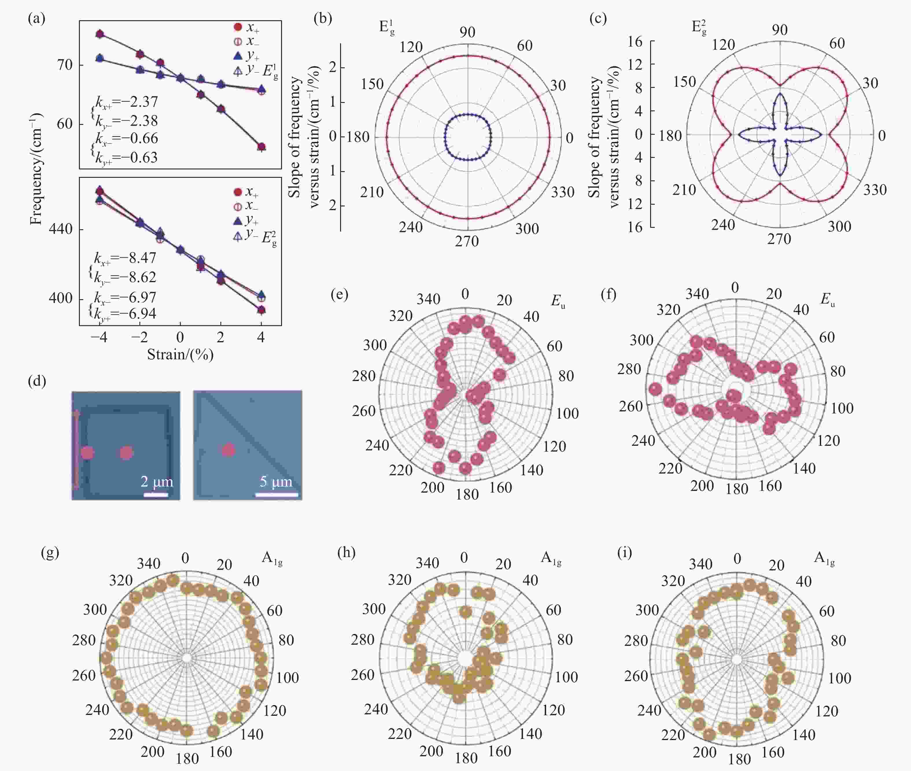
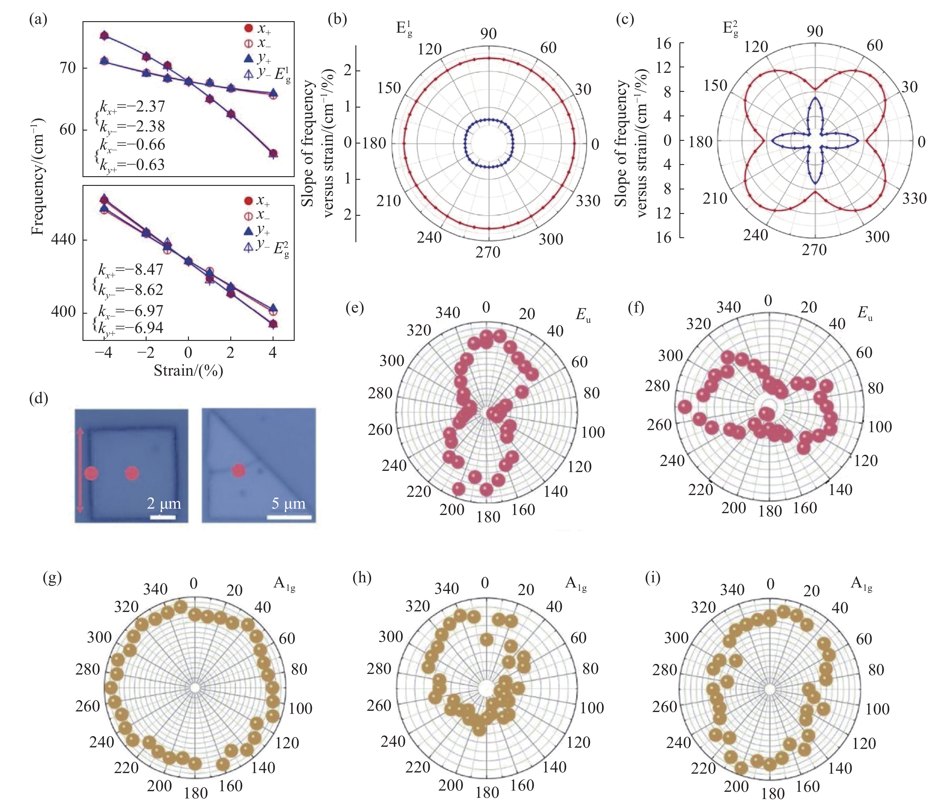
图 7 Bi2O2Se的偏振拉曼光谱(532 nm激光)[41-42]。(a) 块状Bi2O2Se拉曼峰位偏移与单轴应变的关系;(b)
$ {E}_{{g}}^{1} $ ,和(c)${E}_{g}^{t} $ 两种简并模式的拉曼峰位偏移的变化速率与旋转单轴应变的关系;(d) 样品的光学显微镜图像;(e) 和(f) 分别是正方形边缘和直角三角形的内部水平线缺陷处位于~55 cm−1的Eu模式拉曼强度的极坐标。(g-i) 分别是正方形中心、正方形边缘和直角三角形的内部水平线缺陷处位于~160 cm−1的A1g模式拉曼强度的极坐标[41-42]Figure 7. Polarized Raman spectra of Bi2O2Se (532 nm laser)[41-42]. (a) Evolutions of Raman shift with uniaxial strain for bulk Bi2O2Se. (b, c) Raman frequencies changes with rotated uniaxial strain for degenerate (b)
$ {E}_{g}^{1} $ and (c)$ {E}_{g}^{2} $ modes in bulk Bi2O2Se. (d) Optical microscope images of polarization-dependent Raman spectra collected at the center and the edge of the square sample and at the inner horizontal line defect of the right-angled triangle sample. Copyright © 2018, American Chemical Society. (e-f) Polar figures of the Raman intensity of (e) the square edge and (f) triangle defect corresponding to Eu modes located at ~ 55 cm−1. (g-i) Polar of the Raman intensity: (g) the square center, (h) the square edge and (i) triangle defect at the A1g mode (~160 cm−1). Copyright © 2022, American Chemical Society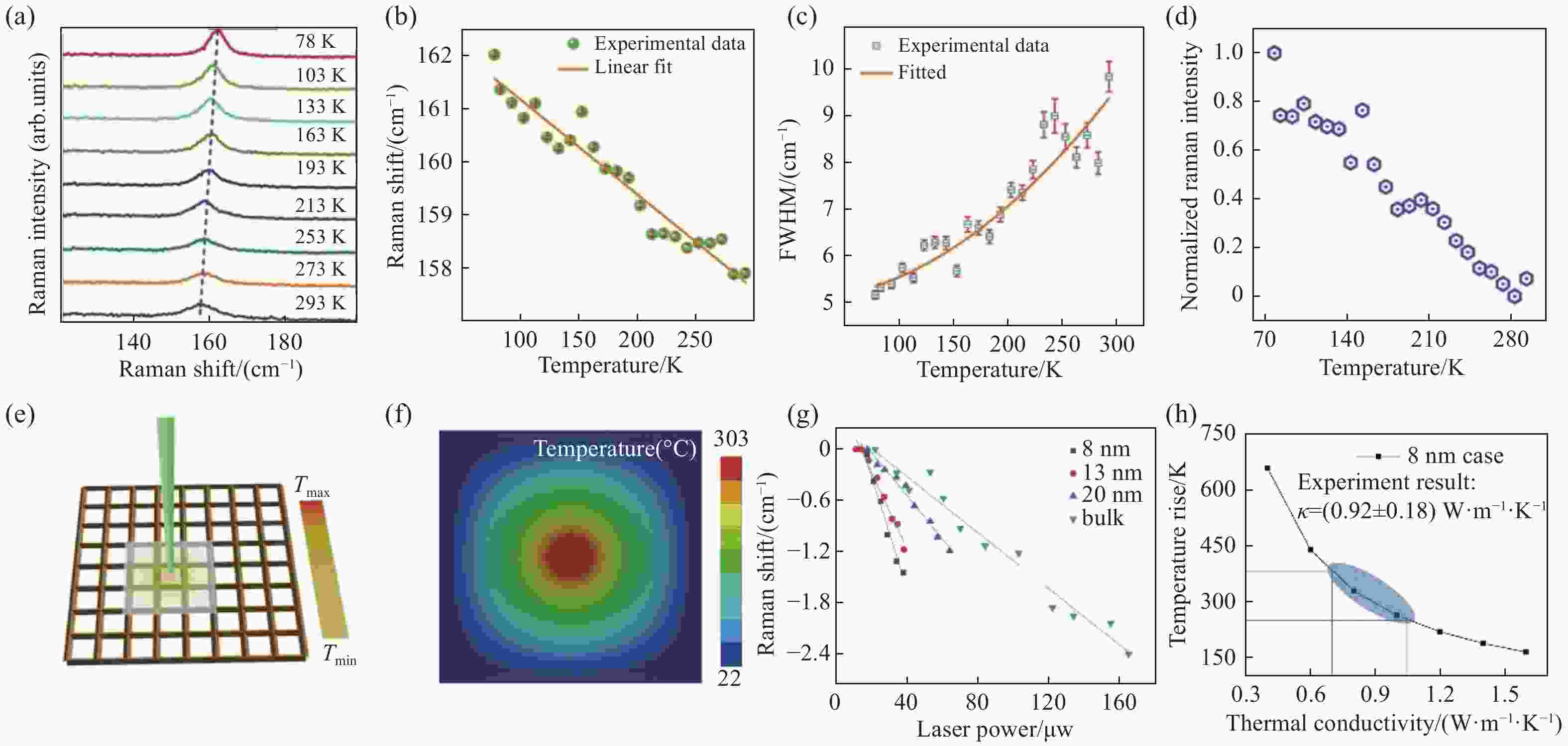
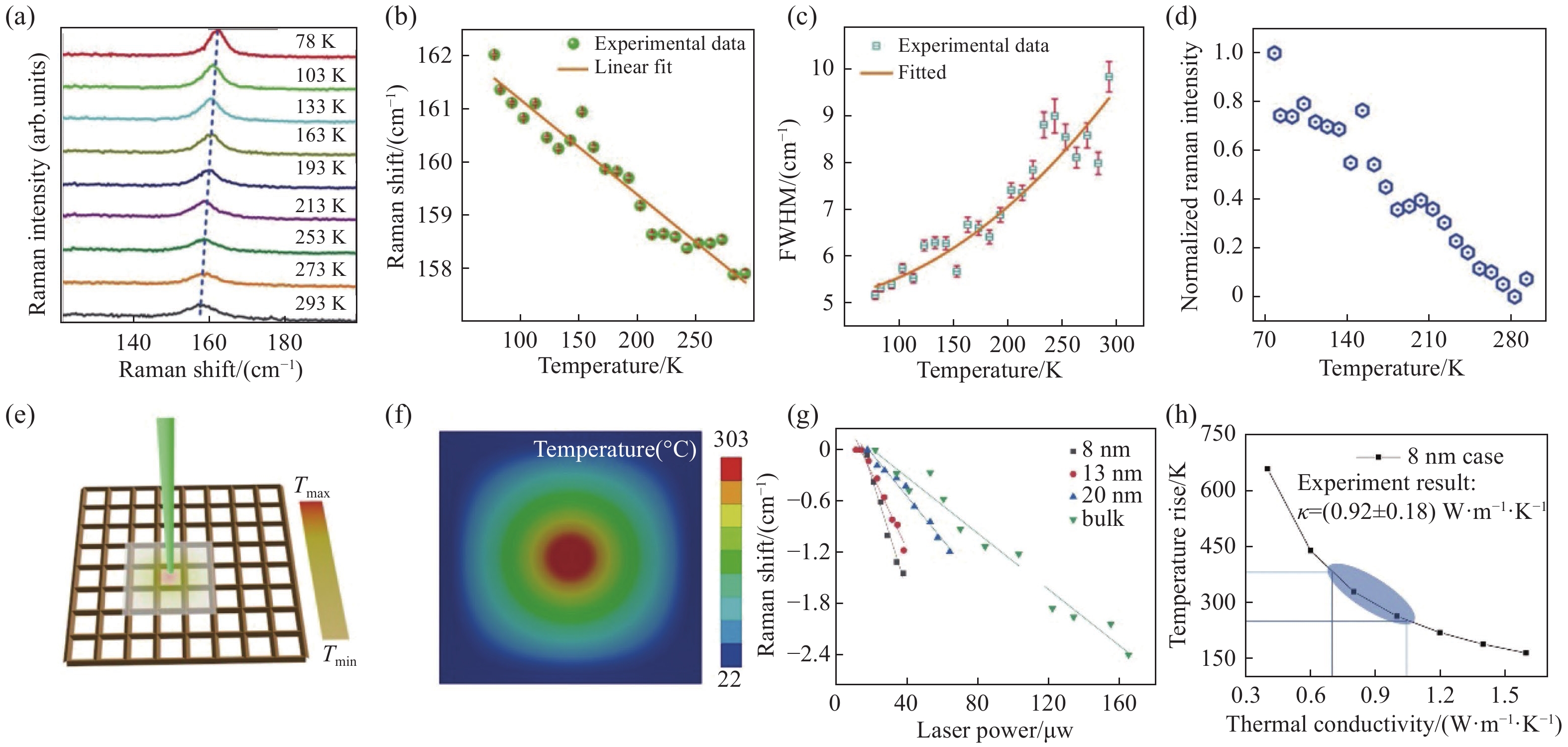
图 8 Bi2O2Se的热效应和热导率[32, 43]。(a) Bi2O2Se纳米片的低温拉曼光谱;(b) Bi2O2Se纳米片的拉曼偏移与温度的关系;(c) A1g模式的FWHM随测量温度的变化[32];(d) A1g模的拉曼强度(归一化处理后)随测量温度的变化;(e) 在光热拉曼测量中,聚焦激光束用作稳态热源,以加热悬浮在Cu网格上的样品的原理图;(f) 稳态下热传导的三维数值建模,图中显示了空间域中的温度和拉曼强度分布;(g) 不同厚度的Bi2O2Se纳米片的A1g峰的峰位与激光功率的关系;(h) 8 nm Bi2O2Se纳米片的平均温升随着稳态下热导率的增加而减小
Figure 8. Thermal effect and thermal conductivity of Bi2O2Se[32, 43]. (a) Low-temperature Raman spectra and (b) corresponding Raman shift as a function of temperature in Bi2O2Se flakes. (c) Variation of FWHM with measurement temperature for the characteristic A1g mode in the semiconducting Bi2O2Se nano-flakes. (d) Variation of Raman intensity of the A1g mode as a function of measurement temperature. Copyright © 2021, AIP Publishing. (e) Schematic of a focused laser beam used as a steady-state heat source to heat a sample suspended on a Cu grid in a photothermal Raman measurement. (f) 3D numerical modeling of the heat conduction at the steady state. Temperature and Raman intensity distribution in the space domain are shown. (g) Power dependence of the A1g peak frequencies of Bi2O2Se flakes with different thicknesses. (h) The average temperature rise of the ~ 8 nm Bi2O2Se flake with increasing thermal conductivity at the steady state. Copyright © 2019, AIP Publishing
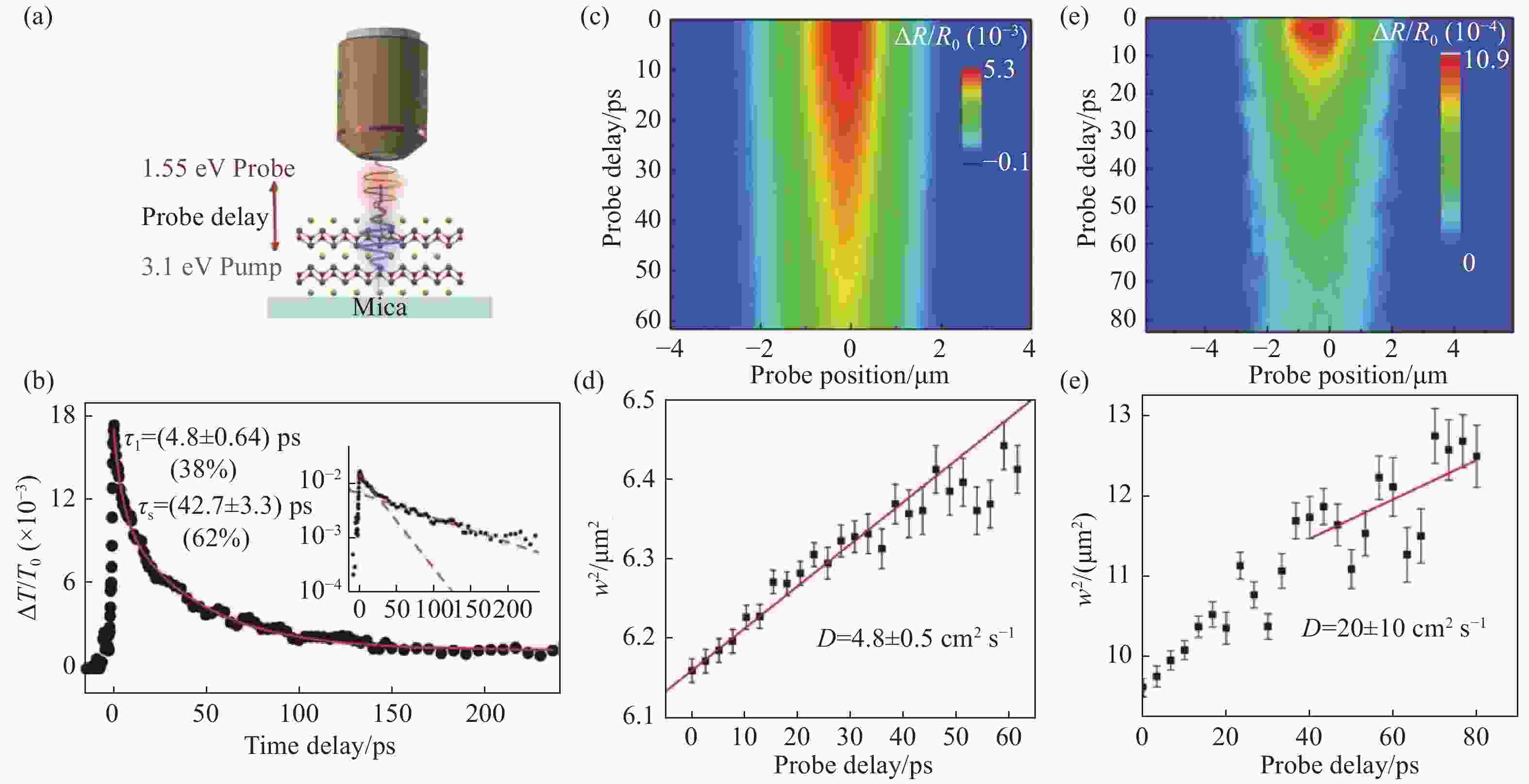
图 9 Bi2O2Se的超快光谱图[44, 45, 115]。(a) 非简并超快泵浦-探测实验示意图。(b) 实验测得的ΔT/T0 (黑色符号)和相应的拟合(红色曲线)。插图显示了带有红色虚线的半对数图,以呈现两个不同的衰减通道。(c)13 nm Bi2O2Se纳米片的差分反射信号。(d) (13 nm的Bi2O2Se纳米片)经高斯拟合得到的由空间剖面取得的半峰宽平方与探测延迟的函数关系。线性拟合(如红线所示)给出的扩散系数约为4.8 cm2s−1。(e)单层Bi2O2Se样品的差分反射信号是探测延迟和探测位置的函数。(f)单层Bi2O2Se高斯拟合得到的空间剖面的平方宽度作为探测延迟的函数。以红线显示的线性拟合得到约20 cm2s−1的扩散系数
Figure 9. Ultrafast spectra of Bi2O2Se[44, 45, 115]. (a) Schematics of non-degenerate ultrafast pump-probe experiment. (b) The measured ΔT/T0 (black symbols) and the corresponding fits (red curves). The inset shows the semi-logarithmic plots with red dotted lines to present two different decay channels. Copyright © 2021, Elsevier. (c) Differential reflection signal of the 13 nm Bi2O2Se nanoplate as a function of both the probe delay and the probe position. (d) The squared width of the spatial profiles obtained by Gaussian fits as a function of the probe delay. The linear fit, shown as the red line, gives a diffusion coefficient of about 4.8 cm2s−1. (e) Differential reflection signal of the monolayer Bi2O2Se sample as a function of both the probe delay and the probe position. (f) The squared width of the spatial profiles obtained by Gaussian fits as a function of the probe delay. The linear fit shown as the red line gives a diffusion coefficient of about 20 cm2/s. Copyright © 2020, John Wiley and Sons
-
[1] BUTLER S Z, HOLLEN S M, CAO L Y, et al. Progress, challenges, and opportunities in two-dimensional materials beyond graphene[J]. ACS Nano, 2013, 7(4): 2898-2926. doi: 10.1021/nn400280c [2] 梁铮, 葛广路, 栾燕, 等. GB/T 30544.13-2018《纳米科技 术语 第13部分: 石墨烯及相关二维材料》核心术语介绍及解读[J]. 中国标准化,2019(S1):23-28.LIANG ZH, GE G L, LUAN Y, et al. Introduction and interpretation of core vocabularies of GB/T 30544.13-2018, nanotechnologies-vocabulary-Part 13: graphene and related two-dimensional (2D) materials[J]. Standardization in China, 2019(S1): 23-28. (in Chinese) [3] LIU Y W, XIAO CH, LI ZH, et al. Vacancy engineering for tuning electron and phonon structures of two-dimensional materials[J]. Advanced Energy Materials, 2016, 6(23): 1600436. doi: 10.1002/aenm.201600436 [4] GUPTA A, SAKTHIVEL T, SEAL S. Recent development in 2D materials beyond graphene[J]. Progress in Materials Science, 2015, 73: 44-126. doi: 10.1016/j.pmatsci.2015.02.002 [5] 张金月, 吕俊鹏, 倪振华. 二维材料异质结高灵敏度红外探测器[J]. 中国光学,2021,14(1):87-99. doi: 10.37188/CO.2020-0139ZHANG J Y, LV J P, NI ZH H. Highly sensitive infrared detector based on a two-dimensional heterojunction[J]. Chinese Optics, 2021, 14(1): 87-99. (in Chinese) doi: 10.37188/CO.2020-0139 [6] NOVOSELOV K S, GEIM A K, MOROZOV S V, et al. Electric field effect in atomically thin carbon films[J]. Science, 2004, 306(5696): 666-669. doi: 10.1126/science.1102896 [7] MAK K F, LEE C, HONE J, et al. Atomically thin MoS2: a new direct-gap semiconductor[J]. Physical Review Letters, 2010, 105(13): 136805. doi: 10.1103/PhysRevLett.105.136805 [8] AYARI A, COBAS E, OGUNDADEGBE O, et al. Realization and electrical characterization of ultrathin crystals of layered transition-metal dichalcogenides[J]. Journal of Applied Physics, 2007, 101(1): 014507. doi: 10.1063/1.2407388 [9] LI L K, YU Y J, YE G J, et al. Black phosphorus field-effect transistors[J]. Nature Nanotechnology, 2014, 9(5): 372-377. doi: 10.1038/nnano.2014.35 [10] MENG L, WANG Y L, ZHANG L ZH, et al. Buckled silicene formation on Ir(111)[J]. Nano Letters, 2013, 13(2): 685-690. doi: 10.1021/nl304347w [11] ZHU P CH, ZHU J. Low-dimensional metal halide perovskites and related optoelectronic applications[J]. InfoMat, 2020, 2(2): 341-378. doi: 10.1002/inf2.12086 [12] NAGUIB M, KURTOGLU M, PRESSER V, et al. Two-dimensional nanocrystals produced by exfoliation of Ti3AlC2[J]. Advanced Materials, 2011, 23(37): 4248-4253. doi: 10.1002/adma.201102306 [13] HONG Y L, LIU ZH B, WANG L, et al. Chemical vapor deposition of layered two-dimensional MoSi2N4 materials[J]. Science, 2020, 369(6504): 670-674. doi: 10.1126/science.abb7023 [14] HUO N J, KONSTANTATOS G. Recent progress and future prospects of 2D-based photodetectors[J]. Advanced Materials, 2018, 30(51): 1801164. doi: 10.1002/adma.201801164 [15] JING X, ILLARIONOV Y, YALON E, et al. Engineering field effect transistors with 2D semiconducting channels: Status and prospects[J]. Advanced Functional Materials, 2020, 30(18): 1901971. doi: 10.1002/adfm.201901971 [16] SANGWAN V K, HERSAM M C. Neuromorphic nanoelectronic materials[J]. Nature Nanotechnology, 2020, 15(7): 517-528. doi: 10.1038/s41565-020-0647-z [17] SHIFA T A, WANG F M, LIU Y, et al. Heterostructures based on 2D materials: A versatile platform for efficient catalysis[J]. Advanced Materials, 2019, 31(45): 1804828. doi: 10.1002/adma.201804828 [18] ZHANG X Y, HOU L L, CIESIELSKI A, et al. 2D materials beyond graphene for high-performance energy storage applications[J]. Advanced Energy Materials, 2016, 6(23): 1600671. doi: 10.1002/aenm.201600671 [19] ZHANG Y B, TANG T T, GIRIT C, et al. Direct observation of a widely tunable bandgap in bilayer graphene[J]. Nature, 2009, 459(7248): 820-823. doi: 10.1038/nature08105 [20] SCHWIERZ F. Graphene transistors[J]. Nature Nanotechnology, 2010, 5(7): 487-496. doi: 10.1038/nnano.2010.89 [21] JARIWALA D, SANGWAN V K, LAUHON L J, et al. Emerging device applications for semiconducting two-dimensional transition metal dichalcogenides[J]. ACS Nano, 2014, 8(2): 1102-1120. doi: 10.1021/nn500064s [22] CUI X, LEE G H, KIM Y D, et al. Multi-terminal transport measurements of MoS2 using a van der Waals heterostructure device platform[J]. Nature Nanotechnology, 2015, 10(6): 534-540. doi: 10.1038/nnano.2015.70 [23] ZHANG SH, YANG J, XU R J, et al. Extraordinary photoluminescence and strong temperature/angle-dependent Raman responses in few-layer phosphorene[J]. ACS Nano, 2014, 8(9): 9590-9596. doi: 10.1021/nn503893j [24] ISLAND J O, STEELE G A, VAN DER ZANT H S, et al. Environmental instability of few-layer black phosphorus[J]. 2D Materials, 2015, 2(1): 011002. doi: 10.1088/2053-1583/2/1/011002 [25] CHEN CH, WANG M X, WU J X, et al. Electronic structures and unusually robust bandgap in an ultrahigh-mobility layered oxide semiconductor, Bi2O2Se[J]. Science Advances, 2018, 4(9): eaat8355. doi: 10.1126/sciadv.aat8355 [26] WU J X, YUAN H T, MENG M M, et al. High electron mobility and quantum oscillations in non-encapsulated ultrathin semiconducting Bi2O2Se[J]. Nature Nanotechnology, 2017, 12(6): 530-534. doi: 10.1038/nnano.2017.43 [27] TIAN X L, LUO H Y, WEI R F, et al. An ultrabroadband Mid-infrared pulsed optical switch employing solution-processed bismuth oxyselenide[J]. Advanced Materials, 2018, 30(31): 1801021. doi: 10.1002/adma.201801021 [28] SONG CH CH, SONG Y L, PAN L, et al. Thermoelectric properties of Bi2-xTixO2Se with the shear exfoliation-restacking process[J]. Journal of Alloys and Compounds, 2022, 892: 162147. doi: 10.1016/j.jallcom.2021.162147 [29] ZHANG Z Y, LI T R, WU Y J, et al. Truly concomitant and independently expressed short-and long-term plasticity in a Bi2O2Se-based three-terminal memristor[J]. Advanced Materials, 2019, 31(3): 1805769. doi: 10.1002/adma.201805769 [30] YANG C M, CHEN T C, VERMA D, et al. Bidirectional all-optical synapses based on a 2D Bi2O2Se/Graphene hybrid structure for multifunctional optoelectronics[J]. Advanced Functional Materials, 2020, 30(30): 2001598. doi: 10.1002/adfm.202001598 [31] WU J X, TAN C W, TAN ZH J, et al. Controlled synthesis of high-mobility atomically thin bismuth oxyselenide crystals[J]. Nano Letters, 2017, 17(5): 3021-3026. doi: 10.1021/acs.nanolett.7b00335 [32] HOSSAIN M T, GIRI P K. Temperature-dependent Raman studies and thermal conductivity of direct CVD grown non-van der Waals layered Bi2O2Se[J]. Journal of Applied Physics, 2021, 129(17): 175102. doi: 10.1063/5.0049368 [33] YANG X, ZHANG Q, SONG Y CH, et al. High mobility two-dimensional bismuth oxyselenide single crystals with large grain size grown by reverse-flow chemical vapor deposition[J]. ACS Applied Materials &Interfaces, 2021, 13(41): 49153-49162. [34] SUN Y, YE S, ZHANG J, et al. Lithium nitrate-assisted hydrothermal synthesis of ultrathin Bi2O2Se nanosheets and their photoelectrochemical performance[J]. Journal of Materials Chemistry C, 2020, 8(42): 14711-14717. doi: 10.1039/D0TC04352D [35] PANG X X, ZHAO Y T, GAO X X, et al. Two-step colloidal synthesis of micron-scale Bi2O2Se nanosheets and their electrostatic assembly for thin-film photodetectors with fast response[J]. Chinese Chemical Letters, 2021, 32(10): 3099-3104. doi: 10.1016/j.cclet.2021.03.039 [36] ZHANG K Y, HU CH G, KANG X L, et al. Synthesis and thermoelectric properties of Bi2O2Se nanosheets[J]. Materials Research Bulletin, 2013, 48(10): 3968-3972. doi: 10.1016/j.materresbull.2013.06.013 [37] LIANG Y, CHEN Y J, SUN Y W, et al. Molecular beam epitaxy and electronic structure of atomically thin oxyselenide films[J]. Advanced Materials, 2019, 31(39): 1901964. doi: 10.1002/adma.201901964 [38] SONG Y K, LI ZH J, LI H, et al. Epitaxial growth and characterization of high quality Bi2O2Se thin films on SrTiO3 substrates by pulsed laser deposition[J]. Nanotechnology, 2020, 31(16): 165704. doi: 10.1088/1361-6528/ab6686 [39] HU C W, YANG Y, HOU CH J, et al. Thickness-and strain-tunable electronic structures of two-dimensional Bi2O2Se[J]. Computational Materials Science, 2021, 194: 110424. doi: 10.1016/j.commatsci.2021.110424 [40] NI Z H, WANG H M, KASIM J, et al. Graphene thickness determination using reflection and contrast spectroscopy[J]. Nano Letters, 2007, 7(9): 2758-2763. doi: 10.1021/nl071254m [41] KIM U J, NAM S H, SEO J, et al. Visualizing line defects in non-van der Waals Bi2O2Se using raman spectroscopy[J]. ACS Nano, 2022, 16(3): 3637-3646. doi: 10.1021/acsnano.1c06598 [42] CHENG T, TAN C W, ZHANG SH Q, et al. Raman spectra and strain effects in bismuth oxychalcogenides[J]. The Journal of Physical Chemistry C, 2018, 122(34): 19970-19980. doi: 10.1021/acs.jpcc.8b05475 [43] YANG F, WANG R D, ZHAO W W, et al. Thermal transport and energy dissipation in two-dimensional Bi2O2Se[J]. Applied Physics Letters, 2019, 115(19): 193103. doi: 10.1063/1.5123682 [44] HAN Y D, LIU Y G, GU CH, et al. Ultrafast carrier dynamics of Bi2O2Se nanoplates in the nonlinear excitation regime[J]. Chemical Physics, 2021, 541: 111017. doi: 10.1016/j.chemphys.2020.111017 [45] LIU SH Y, TAN C W, HE D W, et al. Optical properties and photocarrier dynamics of Bi2O2Se monolayer and nanoplates[J]. Advanced Optical Materials, 2020, 8(6): 1901567. doi: 10.1002/adom.201901567 [46] BOLLER H. Die kristallstruktur von Bi2O2Se[J]. Monatshefte für Chemie/Chemical Monthly, 1973, 104(4): 916-919. [47] RULEOVA P, DRASAR C, LOSTAK P, et al. Thermoelectric properties of Bi2O2Se[J]. Materials Chemistry and Physics, 2010, 119(1-2): 299-302. doi: 10.1016/j.matchemphys.2009.08.067 [48] DRASAR C, RULEOVA P, BENES L, et al. Preparation and transport properties of Bi2O2Se single crystals[J]. Journal of Electronic Materials, 2012, 41(9): 2317-2321. doi: 10.1007/s11664-012-2143-1 [49] PAN L, ZHAO L, ZHANG X X, et al. Significant optimization of electron–phonon transport of n-Type Bi2O2Se by mechanical manipulation of Se vacancies via shear exfoliation[J]. ACS Applied Materials &Interfaces, 2019, 11(24): 21603-21609. [50] ZHAN B, LIU Y CH, TAN X, et al. Enhanced thermoelectric properties of Bi2O2Se ceramics by Bi deficiencies[J]. Journal of the American Ceramic Society, 2015, 98(8): 2465-2469. doi: 10.1111/jace.13619 [51] TAN X, LIU Y CH, LIU R, et al. Synergistical enhancement of thermoelectric properties in n-Type Bi2O2Se by carrier engineering and hierarchical microstructure[J]. Advanced Energy Materials, 2019, 9(31): 1900354. doi: 10.1002/aenm.201900354 [52] ZHAN B, BUTT S, LIU Y CH, et al. High-temperature thermoelectric behaviors of Sn-doped n-type Bi2O2Se ceramics[J]. Journal of Electroceramics, 2015, 34(2): 175-179. [53] ZHAN B, LIU Y CH, LAN J L, et al. Enhanced thermoelectric performance of Bi2O2Se with Ag addition[J]. Materials, 2015, 8(4): 1568-1576. doi: 10.3390/ma8041568 [54] YIN J B, TAN ZH J, HONG H, et al. Ultrafast and highly sensitive infrared photodetectors based on two-dimensional oxyselenide crystals[J]. Nature Communications, 2018, 9: 3311. doi: 10.1038/s41467-018-05874-2 [55] LI J, WANG ZH X, WEN Y, et al. High-performance near-infrared photodetector based on ultrathin Bi2O2Se nanosheets[J]. Advanced Functional Materials, 2018, 28(10): 1706437. doi: 10.1002/adfm.201706437 [56] WEI Q L, LI R P, LIN CH Q, et al. Quasi-two-dimensional se-terminated bismuth oxychalcogenide (Bi2O2Se)[J]. ACS Nano, 2019, 13(11): 13439-13444. doi: 10.1021/acsnano.9b07000 [57] MENG M M, HUANG SH Y, TAN C W, et al. Universal conductance fluctuations and phase-coherent transport in a semiconductor Bi2O2Se nanoplate with strong spin–orbit interaction[J]. Nanoscale, 2019, 11(22): 10622-10628. doi: 10.1039/C9NR02347J [58] FU H X, WU J X, PENG H L, et al. Self-modulation doping effect in the high-mobility layered semiconductor Bi2O2Se[J]. Physical Review B, 2018, 97(24): 241203. doi: 10.1103/PhysRevB.97.241203 [59] TONG T, LI W SH, QIN SH CH, et al. Bi2O2Se/Au-based schottky phototransistor with fast response and ultrahigh responsivity[J]. IEEE Electron Device Letters, 2020, 41(10): 1464-1467. doi: 10.1109/LED.2020.3016186 [60] LUO P, ZHUGE F W, WANG F K, et al. PbSe quantum dots sensitized high-mobility Bi2O2Se nanosheets for high-performance and broadband photodetection beyond 2 μm[J]. ACS Nano, 2019, 13(8): 9028-9037. doi: 10.1021/acsnano.9b03124 [61] WU J X, LIU Y J, TAN ZH J, et al. Chemical patterning of high-mobility semiconducting 2D Bi2O2Se crystals for integrated optoelectronic Devices[J]. Advanced Materials, 2017, 29(44): 1704060. doi: 10.1002/adma.201704060 [62] WU J X, QIU CH G, FU H X, et al. Low residual carrier concentration and high mobility in 2D semiconducting Bi2O2Se[J]. Nano Letters, 2018, 19(1): 197-202. [63] YING J H, HE J B, YANG G, et al. Magnitude and spatial distribution control of the supercurrent in Bi2O2Se-based josephson junction[J]. Nano Letters, 2020, 20(4): 2569-2575. doi: 10.1021/acs.nanolett.0c00025 [64] FU Q D, ZHU CH, ZHAO X X, et al. Ultrasensitive 2D Bi2O2Se phototransistors on silicon substrates[J]. Advanced Materials, 2019, 31(1): 1804945. doi: 10.1002/adma.201804945 [65] TAN C W, TANG M, WU J X, et al. Wafer-scale growth of single-crystal 2D semiconductor on perovskite oxides for high-performance transistors[J]. Nano Letters, 2019, 19(3): 2148-2153. doi: 10.1021/acs.nanolett.9b00381 [66] WU ZH, LIU G L, WANG Y X, et al. Seed‐induced vertical growth of 2D Bi2O2Se nanoplates by chemical vapor transport[J]. Advanced Functional Materials, 2019, 29(50): 1906639. doi: 10.1002/adfm.201906639 [67] KANG M, CHAI H J, JEONG H B, et al. Low-temperature and high-quality growth of Bi2O2Se layered semiconductors via cracking metal–organic chemical vapor deposition[J]. ACS Nano, 2021, 15(5): 8715-8723. doi: 10.1021/acsnano.1c00811 [68] KHAN U, LUO Y T, TANG L, et al. Controlled vapor–solid deposition of millimeter‐size single crystal 2D Bi2O2Se for high‐performance phototransistors[J]. Advanced Functional Materials, 2019, 29(14): 1807979. doi: 10.1002/adfm.201807979 [69] XIONG J Y, CHENG G, LU ZH, et al. BiOCOOH hierarchical nanostructures: Shape-controlled solvothermal synthesis and photocatalytic degradation performances[J]. CrystEngComm, 2011, 13(7): 2381-2390. doi: 10.1039/c0ce00705f [70] LI Y Y, WANG G, ZHU X G, et al. Intrinsic topological insulator Bi2Te3 thin films on Si and their thickness limit[J]. Advanced Materials, 2010, 22(36): 4002-4007. doi: 10.1002/adma.201000368 [71] STOUGHTON S, SHOWAK M, MAO Q, et al. Adsorption-controlled growth of BiVO4 by molecular-beam epitaxy[J]. APL Materials, 2013, 1(4): 042112. doi: 10.1063/1.4824041 [72] LI T R, TU T, SUN Y W, et al. A native oxide high-κ gate dielectric for two-dimensional electronics[J]. Nature Electronics, 2020, 3(8): 473-478. doi: 10.1038/s41928-020-0444-6 [73] LI T R, PENG H L. 2D Bi2O2Se: an emerging material platform for the next-generation electronic industry[J]. Accounts of Materials Research, 2021, 2(9): 842-853. doi: 10.1021/accountsmr.1c00130 [74] LIANG Y, ZHOU X H, LI W, et al. Preparation of two-dimensional [Bi2O2]-based layered materials: Progress and prospects[J]. APL Materials, 2021, 9(6): 060905. doi: 10.1063/5.0052300 [75] TONG T, ZHANG M H, CHEN Y Q, et al. Ultrahigh Hall mobility and suppressed backward scattering in layered semiconductor Bi2O2Se[J]. Applied Physics Letters, 2018, 113(7): 072106. doi: 10.1063/1.5042727 [76] MAO Q H, GENG X D, YANG J F, et al. Synthesis and electrical transport properties of Bi2O2Se single crystals[J]. Journal of Crystal Growth, 2018, 498: 244-247. doi: 10.1016/j.jcrysgro.2018.07.004 [77] YANG S J, LUO P, WANG F K, et al. Van der waals epitaxy of Bi2Te2Se/Bi2O2Se vertical heterojunction for high performance photodetector[J]. Small, 2022, 18(6): 2105211. doi: 10.1002/smll.202105211 [78] LIDE D R. CRC Handbook of Chemistry and Physics[M]. 86th ed. Boca Raton, FL: CRC Press, 2005, 4: 128-129. [79] HORÁK J, STARY Z, LOŠŤÁK P, et al. Anti-site defects in n-Bi2Se3 crystals[J]. Journal of Physics and Chemistry of Solids, 1990, 51(12): 1353-1360. doi: 10.1016/0022-3697(90)90017-A [80] LIU D, GUO Y ZH, FANG L, et al. Sulfur vacancies in monolayer MoS2 and its electrical contacts[J]. Applied Physics Letters, 2013, 103(18): 183113. doi: 10.1063/1.4824893 [81] PADILHA J E, PEELAERS H, JANOTTI A, et al. Nature and evolution of the band-edge states in MoS2: From monolayer to bulk[J]. Physical Review B, 2014, 90(20): 205420. doi: 10.1103/PhysRevB.90.205420 [82] TRAN V, FEI R X, YANG L. Quasiparticle energies, excitons, and optical spectra of few-layer black phosphorus[J]. 2D Materials, 2015, 2(4): 044014. doi: 10.1088/2053-1583/2/4/044014 [83] ZHU X L, LIU P F, XIE G F, et al. First-principles study of thermal transport properties in the two-and three-dimensional forms of Bi2O2Se[J]. Physical Chemistry Chemical Physics, 2019, 21(21): 10931-10938. doi: 10.1039/C9CP01867K [84] YU J B, SUN Q. Bi2O2Se nanosheet: An excellent high-temperature n-type thermoelectric material[J]. Applied Physics Letters, 2018, 112(5): 053901. doi: 10.1063/1.5017217 [85] HONG H Y, KIM D H, WON S O, et al. Enhancement of the thermoelectric performance of n- type Bi2O2Se by Ce4+ doping[J]. Journal of Materials Research and Technology, 2021, 15: 4161-4172. doi: 10.1016/j.jmrt.2021.10.002 [86] XIE B, YANG F, AN X H, et al. . Controlled growth and optical characterization of high mobility layered semiconductor Bi2O2Se. (unpublished) [87] 张雁, 尹利辉, 冯芳. 拉曼光谱分析法的应用介绍[J]. 药物分析杂志,2009,29(7):1236-1241. doi: 10.16155/j.0254-1793.2009.07.001ZHANG Y, YIN L H, FENG F. Introduction for the application of Raman scattering method[J]. Chinese Journal of Pharmaceutical Analysis, 2009, 29(7): 1236-1241. (in Chinese) doi: 10.16155/j.0254-1793.2009.07.001 [88] 侯翔宇, 邱腾. 低维光电材料缺陷与界面增强拉曼散射[J]. 中国光学,2021,14(1):170-181. doi: 10.37188/CO.2020-0145HOU X Y, QIU T. Defects- and interface-enhanced Raman scattering in low-dimensional optoelectronic materials[J]. Chinese Optics, 2021, 14(1): 170-181. (in Chinese) doi: 10.37188/CO.2020-0145 [89] PEREIRA A L J, SANTAMARÍA-PÉREZ D, RUIZ-FUERTES J, et al. Experimental and theoretical Study of Bi2O2Se under compression[J]. The Journal of Physical Chemistry C, 2018, 122(16): 8853-8867. doi: 10.1021/acs.jpcc.8b02194 [90] CHEN SH Y, ZHENG CH X, FUHRER M S, et al. Helicity-resolved Raman scattering of MoS2, MoSe2, WS2, and WSe2 atomic layers[J]. Nano Letters, 2015, 15(4): 2526-2532. doi: 10.1021/acs.nanolett.5b00092 [91] TAN Q H, SUN Y J, LIU X L, et al. Observation of forbidden phonons, Fano resonance and dark excitons by resonance Raman scattering in few-layer WS2[J]. 2D Materials, 2017, 4(3): 031007. doi: 10.1088/2053-1583/aa79bb [92] KIM S, KIM K, LEE J U, et al. Excitonic resonance effects and Davydov splitting in circularly polarized Raman spectra of few-layer WSe2[J]. 2D Materials, 2017, 4(4): 045002. doi: 10.1088/2053-1583/aa8312 [93] LEE J U, WOO S, PARK J, et al. Strain-shear coupling in bilayer MoS2[J]. Nature Communications, 2017, 8(1): 1370. doi: 10.1038/s41467-017-01487-3 [94] KIM J, LEE J U, LEE J, et al. Anomalous polarization dependence of Raman scattering and crystallographic orientation of black phosphorus[J]. Nanoscale, 2015, 7(44): 18708-18715. doi: 10.1039/C5NR04349B [95] HUANG M Y, YAN H G, CHEN CH Y, et al. Phonon softening and crystallographic orientation of strained graphene studied by Raman spectroscopy[J]. Proceedings of the National Academy of Sciences of the United States of America, 2009, 106(18): 7304-7308. doi: 10.1073/pnas.0811754106 [96] WANG Y L, CONG CH X, QIU C Y, et al. Raman spectroscopy study of lattice vibration and crystallographic orientation of monolayer MoS2 under uniaxial strain[J]. Small, 2013, 9(17): 2857-2861. doi: 10.1002/smll.201202876 [97] CONLEY H J, WANG B, ZIEGLER J I, et al. Bandgap engineering of strained monolayer and bilayer MoS2[J]. Nano Letters, 2013, 13(8): 3626-3630. doi: 10.1021/nl4014748 [98] RIBEIRO-SOARES J, ALMEIDA R M, BARROS E B, et al. Group theory analysis of phonons in two-dimensional transition metal dichalcogenides[J]. Physical Review B, 2014, 90(11): 115438. doi: 10.1103/PhysRevB.90.115438 [99] YOU Y M, NI ZH H, YU T, et al. Edge chirality determination of graphene by Raman spectroscopy[J]. Applied Physics Letters, 2008, 93(16): 163112. doi: 10.1063/1.3005599 [100] LEE U, HAN Y, LEE S, et al. Time evolution studies on strain and doping of graphene grown on a copper substrate using Raman spectroscopy[J]. ACS Nano, 2020, 14(1): 919-926. doi: 10.1021/acsnano.9b08205 [101] SAHOO S, MALLIK S K, SAHU M C, et al. Thermal conductivity of free-standing silicon nanowire using Raman spectroscopy[J]. Nanotechnology, 2020, 31(50): 505701. doi: 10.1088/1361-6528/abb42c [102] SAHOO S, GAUR A P S, AHMADI M, et al. Temperature-dependent Raman studies and thermal conductivity of few-layer MoS2[J]. The Journal of Physical Chemistry C, 2013, 117(17): 9042-9047. doi: 10.1021/jp402509w [103] ZHANG X, SUN D ZH, LI Y L, et al. Measurement of lateral and interfacial thermal conductivity of single-and bilayer MoS2 and MoSe2 using refined optothermal Raman technique[J]. ACS Applied Materials &Interfaces, 2015, 7(46): 25923-25929. [104] PEIMYOO N, SHANG J ZH, YANG W H, et al. Thermal conductivity determination of suspended mono-and bilayer WS2 by Raman spectroscopy[J]. Nano Research, 2015, 8(4): 1210-1221. doi: 10.1007/s12274-014-0602-0 [105] LANZILLO N A, BIRDWELL A G, AMANI M, et al. Temperature-dependent phonon shifts in monolayer MoS2[J]. Applied Physics Letters, 2013, 103(9): 093102. doi: 10.1063/1.4819337 [106] BALKANSKI M, WALLIS R F, HARO E. Anharmonic effects in light scattering due to optical phonons in silicon[J]. Physical Review B, 1983, 28(4): 1928-1934. doi: 10.1103/PhysRevB.28.1928 [107] NILSSON G, NELIN G. Phonon dispersion relations in Ge at 80 K[J]. Physical Review B, 1971, 3(2): 364-369. doi: 10.1103/PhysRevB.3.364 [108] BALANDIN A A, GHOSH S, BAO W ZH, et al. Superior thermal conductivity of single-layer graphene[J]. Nano Letters, 2008, 8(3): 902-907. doi: 10.1021/nl0731872 [109] LUO Z, MAASSEN J, DENG Y X, et al. Anisotropic in-plane thermal conductivity observed in few-layer black phosphorus[J]. Nature Communications, 2015, 6(1): 8572. doi: 10.1038/ncomms9572 [110] HUANG L B, HARTLAND G V, CHU L Q, et al. Ultrafast transient absorption microscopy studies of carrier dynamics in epitaxial graphene[J]. Nano Letters, 2010, 10(4): 1308-1313. doi: 10.1021/nl904106t [111] YU J H, SHARMA M, SHARMA A, et al. All-optical control of exciton flow in a colloidal quantum well complex[J]. Light:Science &Applications, 2020, 9: 27. [112] YU J H, HOU S Y, SHARMA M, et al. Strong plasmon-wannier mott exciton interaction with high aspect ratio colloidal quantum wells[J]. Matter, 2020, 2(6): 1550-1563. doi: 10.1016/j.matt.2020.03.013 [113] YU J H, SHENDRE S, KOH W K, et al. Electrically control amplified spontaneous emission in colloidal quantum dots[J]. Science Advances, 2019, 5(10): eaav3140. doi: 10.1126/sciadv.aav3140 [114] 王云坤, 李耀龙, 高宇南. 二维过渡金属硫族化合物中的缺陷和相关载流子动力学的研究进展[J]. 中国光学,2021,14(1):18-42. doi: 10.37188/CO.2020-0106WANG Y K, LI Y L, GAO Y N. Progress on defect and related carrier dynamics in two-dimensional transition metal chalcogenides[J]. Chinese Optics, 2021, 14(1): 18-42. (in Chinese) doi: 10.37188/CO.2020-0106 [115] SUNDARAM S K, MAZUR E. Inducing and probing non-thermal transitions in semiconductors using femtosecond laser pulses[J]. Nature Materials, 2002, 1(4): 217-224. doi: 10.1038/nmat767 [116] SCHÄFER S, LIANG W X, ZEWAIL A H. Primary structural dynamics in graphite[J]. New Journal of Physics, 2011, 13(6): 063030. doi: 10.1088/1367-2630/13/6/063030 [117] RUZICKA B A, WERAKE L K, SAMASSEKOU H, et al. Ambipolar diffusion of photoexcited carriers in bulk GaAs[J]. Applied Physics Letters, 2010, 97(26): 262119. doi: 10.1063/1.3533664 [118] KUMAR N, CUI Q N, CEBALLOS F, et al. Exciton-exciton annihilation in MoSe2 monolayers[J]. Physical Review B, 2014, 89(12): 125427. doi: 10.1103/PhysRevB.89.125427 [119] SUN D ZH, RAO Y, REIDER G A, et al. Observation of rapid exciton–exciton annihilation in monolayer molybdenum disulfide[J]. Nano Letters, 2014, 14(10): 5625-5629. doi: 10.1021/nl5021975 [120] YUAN L, HUANG L B. Exciton dynamics and annihilation in WS2 2D semiconductors[J]. Nanoscale, 2015, 7(16): 7402-7408. doi: 10.1039/C5NR00383K -

 下载:
下载:


计量
- 文章访问数: 3123
- HTML全文浏览量: 1255
- PDF下载量: 743
- 被引次数: 0
