


Relationship between the preparation process of the graphene/silicon hetero-junction photodetector and its voltage-current characteristics
-
摘要:
通过湿法转移二维材料与半导体衬底形成异质结是一种制备异质结光电探测器的常见方法。在湿法转移制备异质结的过程中,不同的制备工艺细节对二维材料与半导体形成的异质结的性能有显著影响。本文以典型的二维材料石墨烯(Gr)为例,采用湿法转移制备了一系列相同的Gr/Si异质结光电探测器,对其制备工艺与伏安特性的关系进行了详细研究。实验结果显示,梯度式烘干工艺可以显著降低Gr/Si异质结器件的暗电流,最佳的烘干温度峰值为170 °C,170 °C 以上漏电流基本不再有变化。Gr/Si范德华异质结表面杂质与夹层中的残留水分对异质结的漏电流有显著影响。 Gr/Si范德华异质结的选择性刻蚀和退火工艺也能够大幅降低漏电流。因此,合适的烘干工艺、选择性刻蚀工艺、退火工艺在Gr/Si异质结器件的制备过程中非常必要。这些结果对于使用湿法转移方法制备二维材料异质结器件具有一定的参考价值。
Abstract:Wet transferring two-dimension (2D) material to a semiconductor substrate is a common method to prepare a hetero-junction photodetector. When preparing to wet transfer a hetero-junction, different preparation details have significant effects on the properties of the hetero-junction formed by the 2D materials and semiconductors. In this paper, a series of identical Gr/Si hetero-junction devices were prepared by the wet transfer method and the relationship between its preparation technique and the voltage-current characteristics was studied in detail. The experimental results show that the gradient drying process can significantly reduce the dark current of the Gr/Si hetero-junction photodetector, the optimal drying temperature peak is 170 °C, and the leakage current basically no longer changes above 170 °C. The surface impurities and residual water in the inter-layer of Gr/Si van der Waals hetero-junction has a significant effect on the leakage current of the hetero-junction. The selective etching and annealing process of a Gr/Si van der Waals hetero-junction can also greatly reduce the leakage current. Therefore, a suitable drying process, selective etching process and annealing process are each necessary in the preparation of a Gr/Si hetero-junction photodetector. These results can give reference to the fabrication of two-dimensional material hetero-junction devices by the wet transfer method.
-
Key words:
- graphene /
- hetero-junction /
- preparation technology /
- voltage-current characteristics /
- drying /
- etching /
- annealing
-
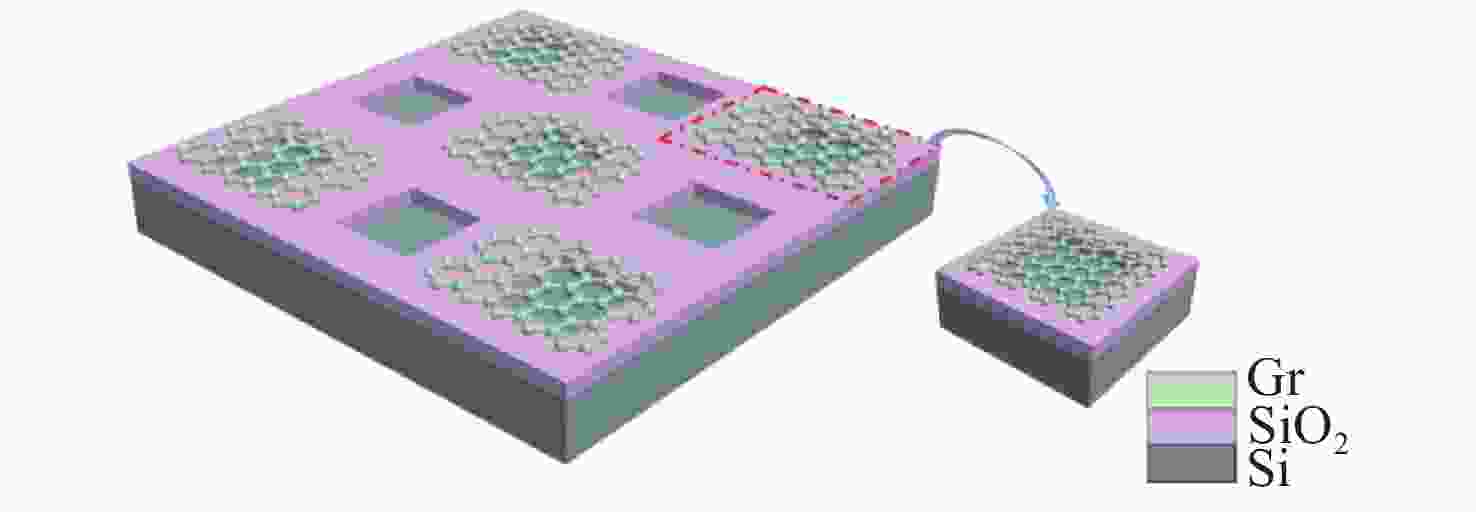
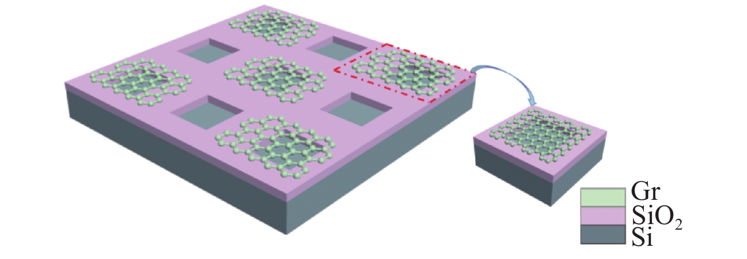
图 1 Gr/Si异质结光电探测器结构示意图
Figure 1. Structural diagram of Gr/Si hetero-junction photodetector
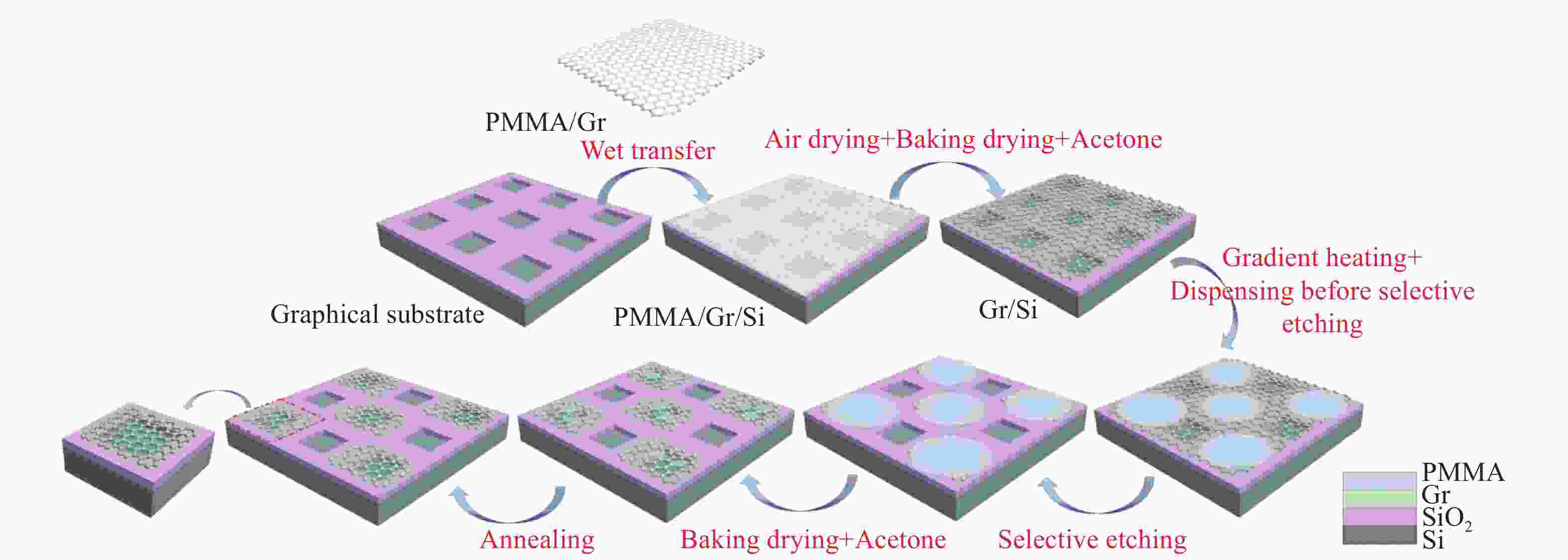
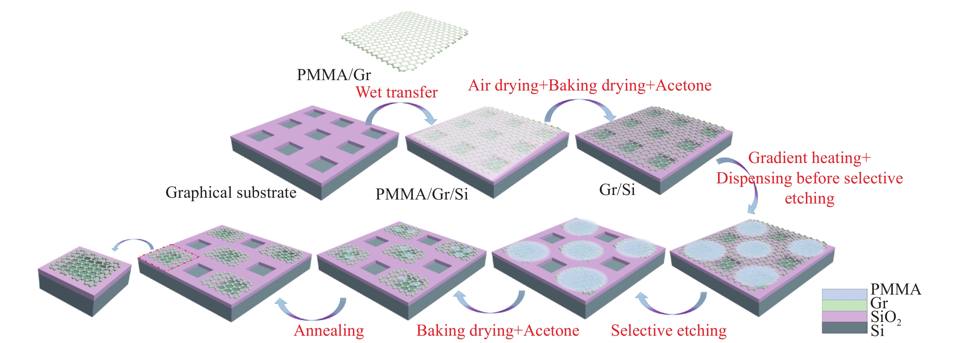
图 2 Gr/Si异质结光电探测器制备工艺流程图
Figure 2. Flow chart of Gr/ Si hetero-junction photodetector preparation
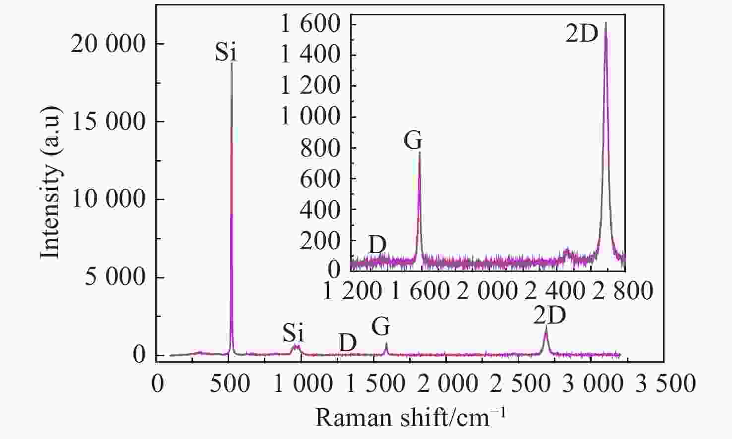
图 3 转移到图形化Si衬底表面的Gr拉曼谱图
Figure 3. The Raman spectrum of the Gr transfered to a patterned Si substrate surface
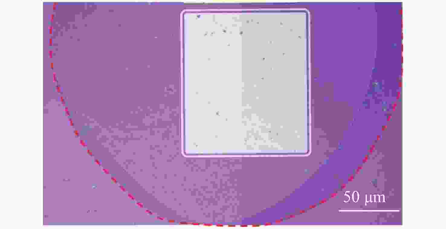
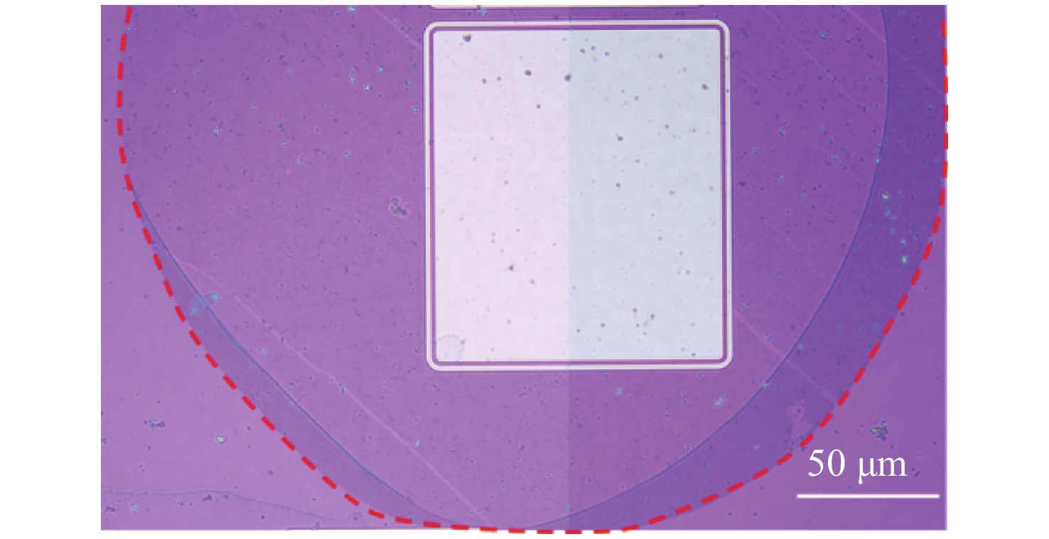
图 4 选择性刻蚀退火后的Gr/Si异质结整体金相显微图(石墨烯边界沿着红色虚线圆圈)
Figure 4. The metallographic micrograph of the Gr/Si hetero-junction after selective etching annealing (graphene boundary along the red dotted circles)
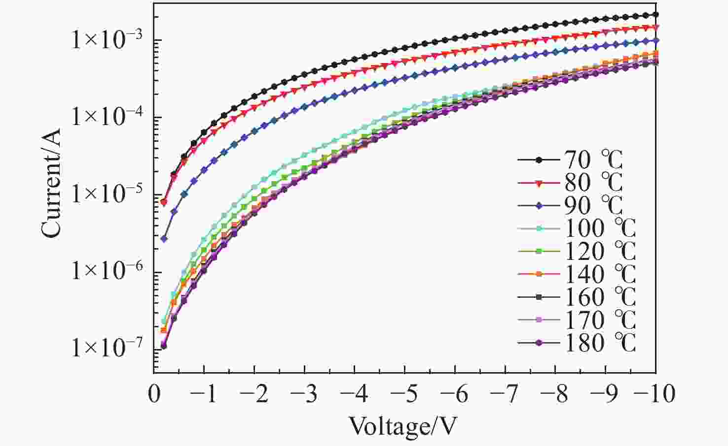
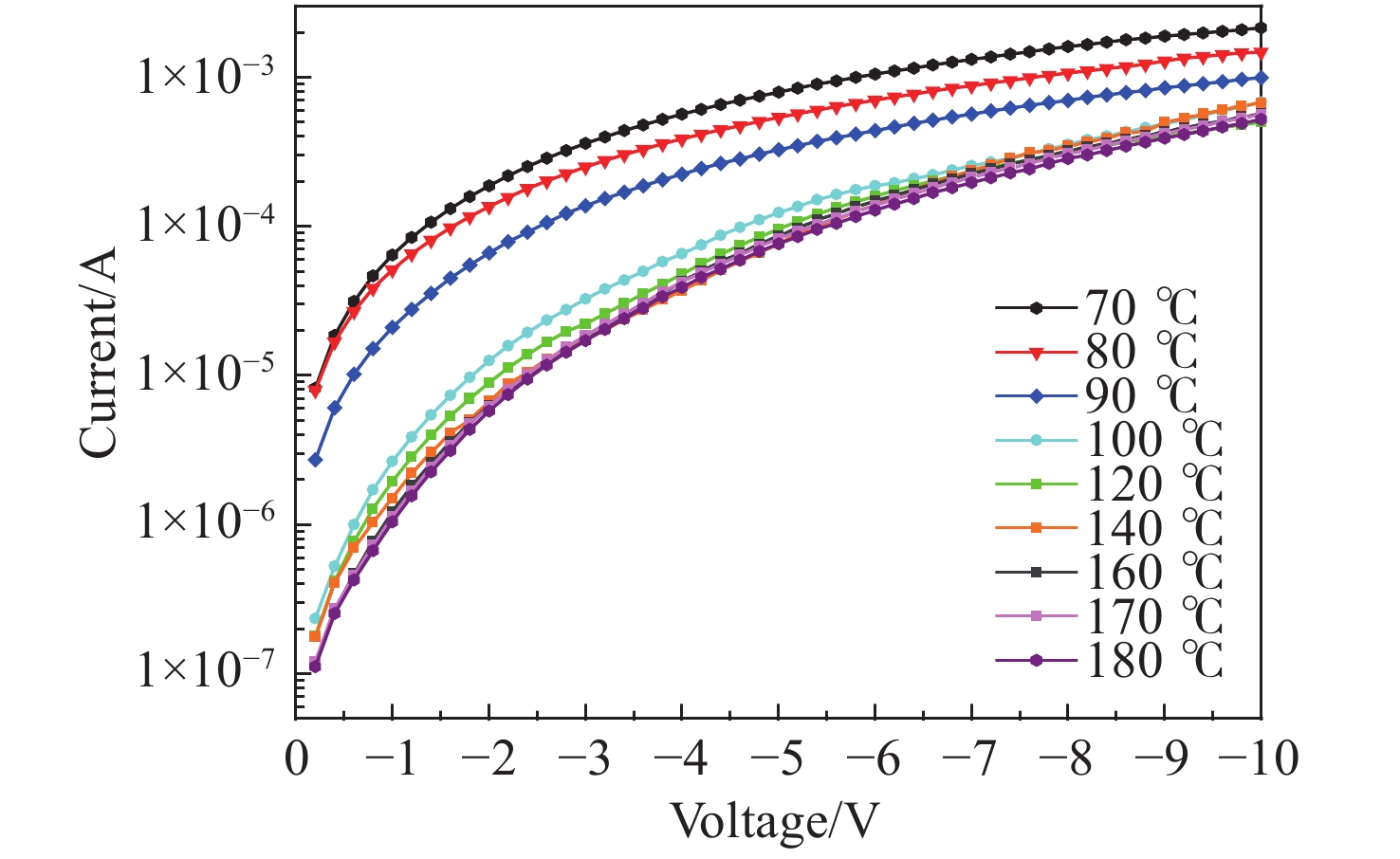
图 5 不同烘干温度条件下选择性刻蚀前大面积Gr/Si异质结的反向伏安特性曲线对比(黑暗遮光条件下测试)
Figure 5. Comparison of the reverse voltage-current characteristic of large area Gr/Si hetero-junction at different drying temperatures ( before selective etching under dark condition)

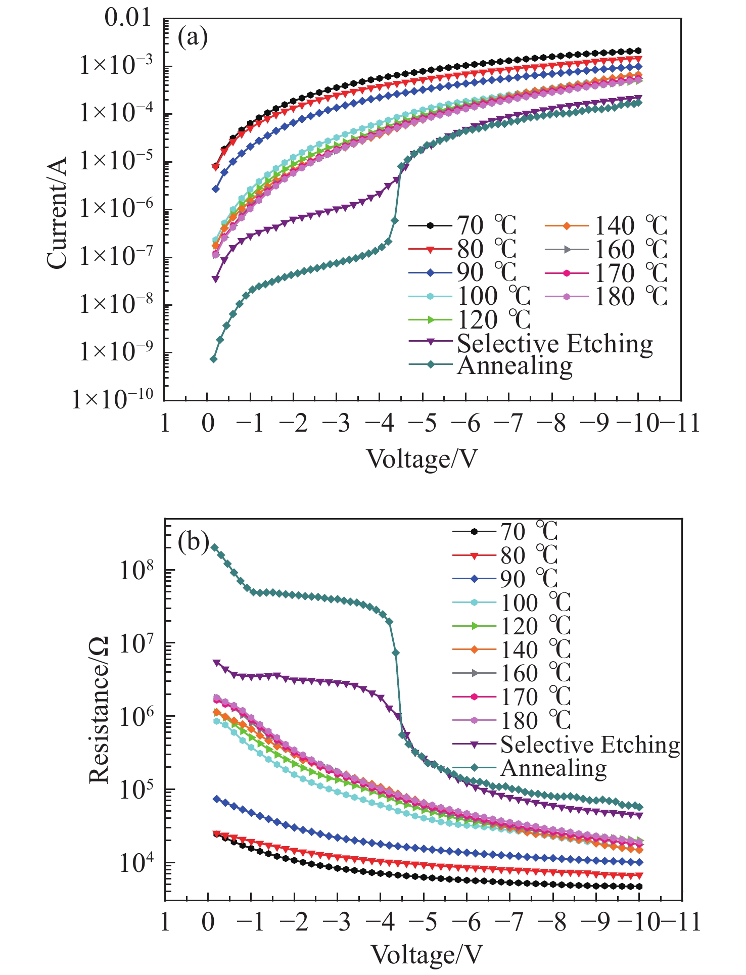
图 6 (a) 不同烘干温度、刻蚀、退火工艺条件下Gr/Si异质结的反向I-V曲线对比; (b) 不同烘干温度、刻蚀、退火工艺条件下Gr/Si异质结的电阻随偏压变化曲线对比(黑暗条件下测试)
Figure 6. (a) Comparison of the reverse voltage-current characteristics of Gr/Si hetero-junction under different drying temperatures, etching and annealing processes; (b) comparison of the voltage-resistance characteristics of Gr/Si hetero-junction under different drying temperatures, etching and annealing processes( under dark condition )
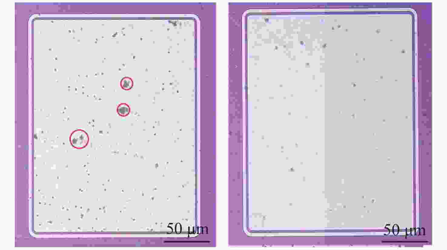
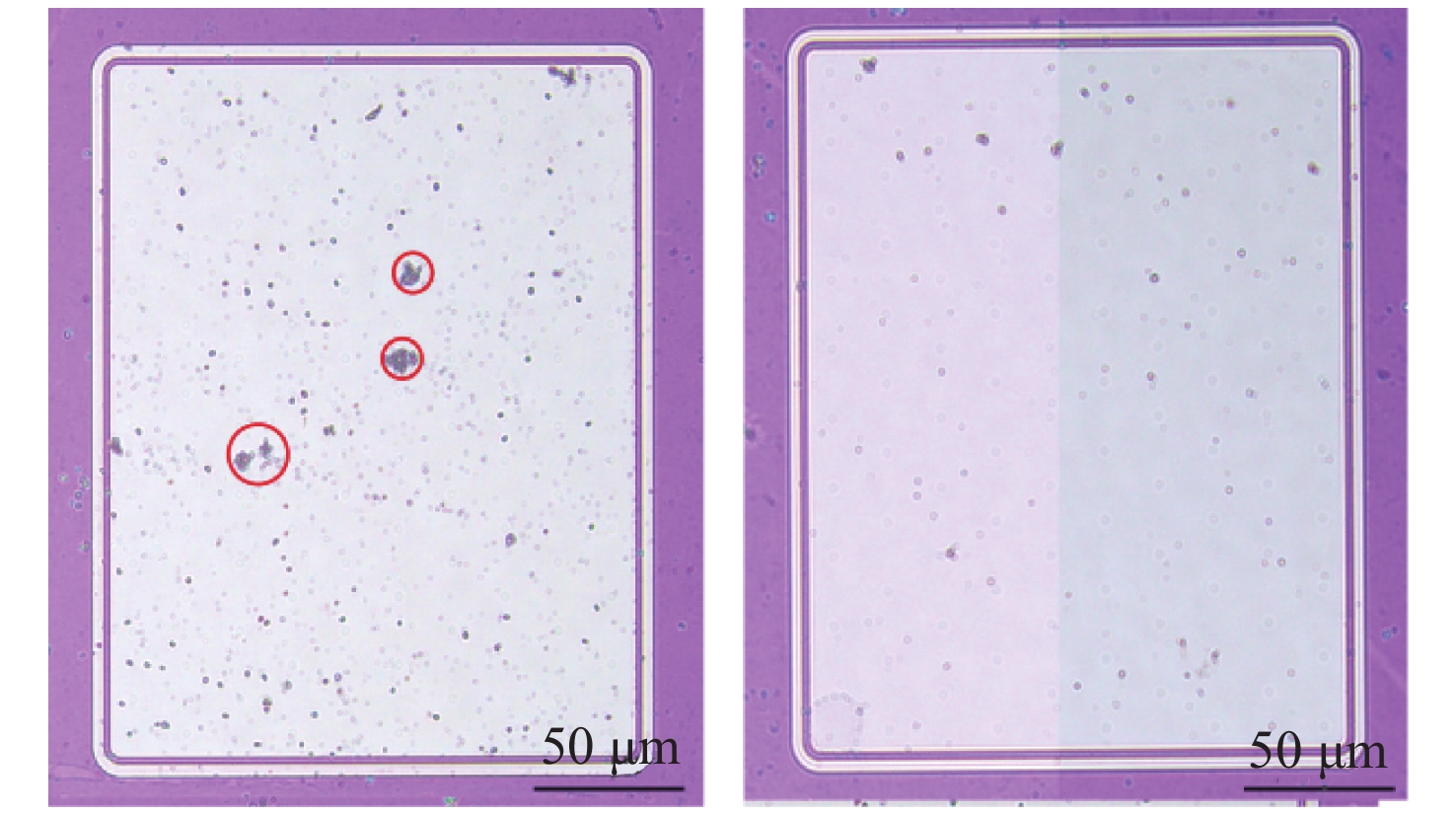
图 7 选择性刻蚀后与退火后异质结表面金相显微图(左为刻蚀后,右为退火后,红色圆圈内为较明显的可挥发性杂质或可能残留的PMMA胶)
Figure 7. Metallographic micrograph of the surface of the hetero-junction after selective etching and annealing (left: after etching, right: after annealing. Red circles are relative obvious volatile impurities or possible residual PMMA glue)
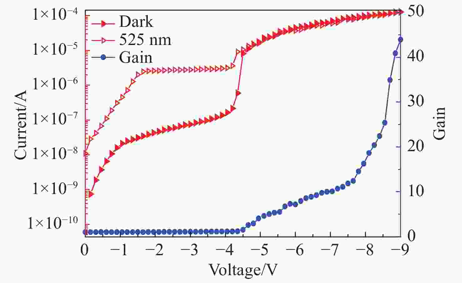
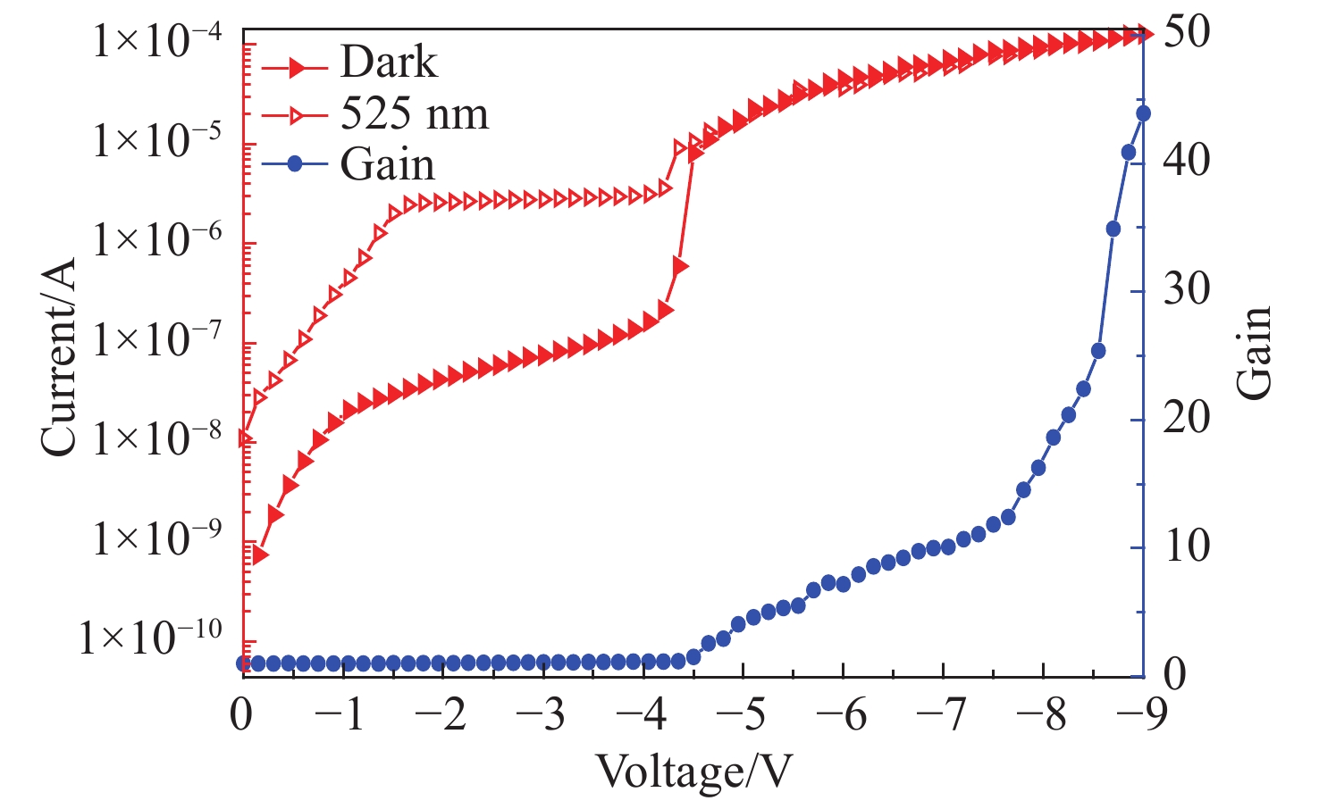
图 8 选择性刻蚀、退火后Gr/Si异质结的反偏伏安特性与增益曲线
Figure 8. Reverse voltage-current characteristics and gain curves of Gr/ Si hetero-junction after selective etching and annealing
-
[1] 朱淼. 石墨烯/硅异质结光电探测器性能研究[D]. 北京: 清华大学, 2015.ZHU M. Study on the graphene/silicon heterojucntion photodetectors[D]. Beijing: Tsinghua University, 2015. (in Chinese) [2] 张翼鹏, 王雪, 纪佩璇, 等. 不同响应机制下的石墨烯基光电探测器研究进展[J]. 发光学报,2022,43(4):552-575. doi: 10.37188/CJL.20210359ZHANG Y P, WANG X, JI P X, et al. Research progress of graphene based photodetectors under different response mechanisms[J]. Chinese Journal of Luminescence, 2022, 43(4): 552-575. (in Chinese) doi: 10.37188/CJL.20210359 [3] 公爽, 田金荣, 李克轩, 等. 新型二维材料在固体激光器中的应用研究进展[J]. 中国光学,2018,11(1):18-30. doi: 10.3788/co.20181101.0018GONG SH, TIAN J R, LI K X, et al. Advances in new two-dimensional materials and its application in solid-state lasers[J]. Chinese Opticas, 2018, 11(1): 18-30. (in Chinese) doi: 10.3788/co.20181101.0018 [4] 胡思奇, 田睿娟, 甘雪涛. 面向硅基光电子混合集成的二维材料探测器[J]. 中国光学,2021,14(5):1039-1055. doi: 10.37188/CO.2021-0003HU S Q, TIAN R J, GAN X T. Two-dimensional material photodetector for hybrid silicon photonics[J]. Chinese Optics, 2021, 14(5): 1039-1055. (in Chinese) doi: 10.37188/CO.2021-0003 [5] YIN J, LIU L, ZANG Y SH, et al. Engineered tunneling layer with enhanced impact ionization for detection improvement in graphene/silicon heterojunction photodetectors[J]. Light:Science &Applications, 2021, 10(1): 113. [6] LI X M, ZHU M, DU M D, et al. High detectivity graphene-silicon heterojunction photodetector[J]. Small, 2016, 12(5): 595-601. doi: 10.1002/smll.201502336 [7] 王学军. 基于二维纳米材料生物传感及光电探测技术的研究[D]. 上海: 华东理工大学, 2018.WANG X J. Two-dimensional nanomaterials for biosensing and photosensing[D]. Shanghai: East China University of Science and Technology, 2018. (in Chinese) [8] LI F, ZHENG J B, YAO Q, et al. Recent progress of silicon integrated light emitters and photodetectors for optical communication based on two-dimensional materials[J]. Optical Materials Express, 2021, 11(10): 3298-3320. doi: 10.1364/OME.435902 [9] GUPTA S, KUMAR R. Review—photodetection properties of graphene/silicon van der Waals heterojunction[J]. ECS Journal of Solid State Science and Technology, 2022, 11(6): 061010. doi: 10.1149/2162-8777/ac7614 [10] 韩天亮, 唐利斌, 左文彬, 等. 石墨烯异质结及其光电器件的研究进展[J]. 红外技术,2021,43(12):1141-1157.HAN T L, TANG L B, ZUO W B, et al. Research progress of graphene heterojunctions and their optoelectronic devices[J]. Infrared Technology, 2021, 43(12): 1141-1157. (in Chinese) [11] DAVYDOVSKAYA D. Photoconductivity in high-quality graphene[D]. Barcelona: Universitat Politècnica de Catalunya, 2015. [12] 张金月, 吕俊鹏, 倪振华. 二维材料异质结高灵敏度红外探测器[J]. 中国光学,2021,14(1):87-99. doi: 10.37188/CO.2020-0139ZHANG J Y, LYU J P, NI ZH H. Highly sensitive infrared detector based on a two-dimensional heterojunction[J]. Chinese Optics, 2021, 14(1): 87-99. (in Chinese) doi: 10.37188/CO.2020-0139 [13] AESCHLIMANN S, ROSSI A, CHÁVEZ-CERVANTES M, et al. Direct evidence for efficient ultrafast charge separation in epitaxial WS2/graphene heterostructures[J]. Science Advances, 2020, 6(20): eaay0761. doi: 10.1126/sciadv.aay0761 [14] ULLAH S, YANG X Q, TA H Q, et al. Graphene transfer methods: a review[J]. Nano Research, 2021, 14(11): 3756-3772. doi: 10.1007/s12274-021-3345-8 [15] 杨珏晗, 魏钟鸣, 牛智川. 基于二维材料异质结的光探测器研究进展[J]. 人工晶体学报,2020,49(3):379-397. doi: 10.3969/j.issn.1000-985X.2020.03.001YANG J H, WEI ZH M, NIU ZH CH. Recent progress on two-dimensional heterostructure based photodetectors[J]. Journal of Synthetic Crystals, 2020, 49(3): 379-397. (in Chinese) doi: 10.3969/j.issn.1000-985X.2020.03.001 [16] 廖俊懿, 吴娟霞, 党春鹤, 等. 二维材料的转移方法[J]. 物理学报,2021,70(2):028201. doi: 10.7498/aps.70.20201425LIAO J Y, WU J X, DANG CH H, et al. Methods of transferring two-dimensional materials[J]. Acta Physica Sinica, 2021, 70(2): 028201. (in Chinese) doi: 10.7498/aps.70.20201425 [17] 吴玉玲, 毕瑞可, 张杰, 等. 石墨烯湿法转移过程工艺优化[J]. 微纳电子技术,2017,54(8):565-569,579.WU Y L, BI R K, ZHANG J, et al. Optimization of the wet transfer technique of graphene[J]. Micronanoelectronic Technology, 2017, 54(8): 565-569,579. (in Chinese) [18] 李春, 胡晓影, 何天应, 等. 二维原子晶体半导体转移技术研究进展[J]. 深圳大学学报理工版,2018,35(3):257-266. doi: 10.3724/SP.J.1249.2018.03257LI CH, HU X Y, HE T Y, et al. Recent progress on transfer techniques of two-dimensional atomically thin semiconductor[J]. Journal of Shenzhen University Science and Engineering, 2018, 35(3): 257-266. (in Chinese) doi: 10.3724/SP.J.1249.2018.03257 [19] 徐杨, 万霞, 郭宏伟, 等. 基于石墨烯/二氧化硅/硅的雪崩光电探测器及制备方法: 中国, CN104300027A[P]. 2015-01-21.XU Y, WAN X, GUO H W, et al. . Avalanche photodetector and preparation method based on graphene/silica/silicon: CN, 104300027A[P]. 2015-01-21. (in Chinese) [20] 王雪. 基于石墨烯/硅肖特基结的光电探测器的研制[D]. 杭州: 浙江大学, 2016.WANG X. Photodetectors based on graphene/silicon schottky diode[D]. Hangzhou: Zhejiang University, 2016. (in Chinese) [21] WANG Y M, YANG SH M, LAMBADA D R, et al. A graphene-silicon Schottky photodetector with graphene oxide interlayer[J]. Sensors and Actuators A:Physical, 2020, 314: 112232. doi: 10.1016/j.sna.2020.112232 [22] LIANG X L, SPERLING B A, CALIZO I, et al. Toward clean and crackless transfer of graphene[J]. ACS Nano, 2011, 5(11): 9144-9153. doi: 10.1021/nn203377t [23] HAN J Y, WANG J. Photodetectors based on two-dimensional materials and organic thin-film heterojunctions[J]. Chinese Physics B, 2019, 28(1): 017103. doi: 10.1088/1674-1056/28/1/017103 [24] 李云杰, 付津滔, 聂长斌, 等. 石墨烯/硅异质结光电导型探测器光电响应及噪声[J]. 微纳电子技术,2022,59(8):732-741. doi: 10.13250/j.cnki.wndz.2022.08.002LI Y J, FU J T, NIE CH B, et al. Photoresponse and noise of graphene/silicon heterojunction photoconductive detector[J]. Micronanoelectronic Technology, 2022, 59(8): 732-741. (in Chinese) doi: 10.13250/j.cnki.wndz.2022.08.002 -

 下载:
下载:


计量
- 文章访问数: 820
- HTML全文浏览量: 640
- PDF下载量: 250
- 被引次数: 0
