


Integrated Nitride optoelectronic chip for motion detection and visible light communication
doi: 10.37188/CO.2023-0028
-
摘要:
在自然界中,物体运动无处不在,随着智能汽车、6G移动通信的高速发展,对通信和运动探测传感融合的高集成度通感一体器件的需求日益增加。本文基于氮化镓多量子阱结构发光和探测并存的特点,提出了一种基于蓝宝石衬底外延生长氮化镓多量子阱材料的集成式光电子芯片,该芯片具有灵敏的运动探测功能及可见光通信功能。该光电子芯片发射器向运动的目标物体发射蓝光波段可见光信号,经目标物体运动调制的可见光信号反射回光电子芯片的接收器部分,激发变化的光电流。通过分析接收器的光电流变化,可探测以不同速度旋转的目标物体的运动情况,光电流曲线变化周期与目标物体旋转周期一致。本文还研究了光电子芯片的各项光电指标及可见光通信性能,该芯片可用作可见光通信系统的收发终端,可以处理和传输芯片采集到的运动探测信号。基于氮化镓多量子阱材料的光电子芯片是一种具有实用价值的高集成度通感一体终端器件。
Abstract:The movement of objects is everywhere in nature. With the rapid development of smart vehicle and 6G mobile communications, the demand for highly Integrated Sensing and Communication (ISAC) devices with communication and motion sensing is increasing. Based on the coexistence of luminescence and detection characteristics of GaN multiple quantum wells, an integrated optoelectronic chip based on the epitaxial GaN multiple quantum wells material on sapphire substrate with sensitive motion detection and visible light communication. The transmitter of the optoelectronic chip transmits a visible light signal in blue band to the moving target object. The visible light signal modulated by the motion of the target object is reflected back to the receiver of the chip to stimulate the changing photocurrent. By analyzing the changing photocurrent, the motion of the target object rotating at different speeds can be detected. The change period of the photocurrent curve is consistent with the rotation period of the target object. We also study the optoelectronic characteristics and the visible light communication performance of the optoelectronic chip. This chip can be used as transceiver terminal of visible light communication system and can also process and transmit the motion detection signals collected by the chip. The optoelectronic chip based on GaN multiple quantum wells materials is a highly integrated ISAC terminal device with application value.
-

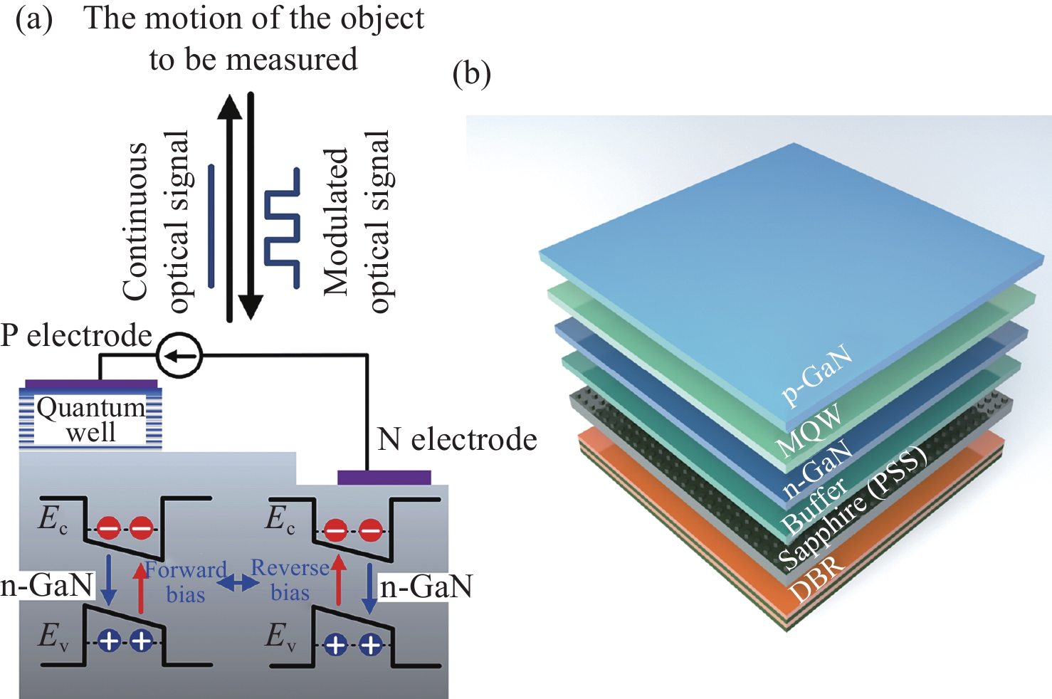
图 1 (a)可实现光电/电光信号双向转换带有多量子阱结构的GaN材料;(b) III族氮化物多量子阱材料的分层结构
Figure 1. (a) GaN materials with multiple quantum wells can realize the bi-directional conversion of optoelectronic/electro-optic signals; (b) layered structure of III-nitride materials with multiple quantum wells
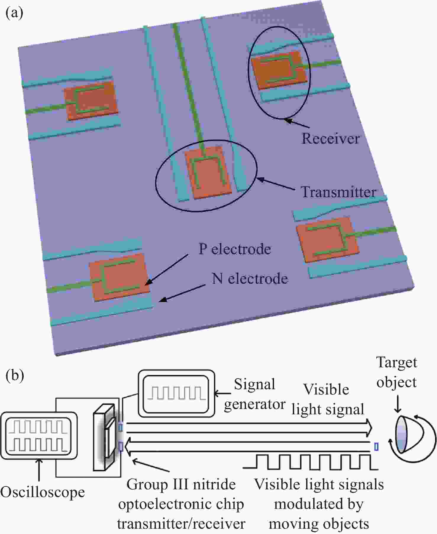
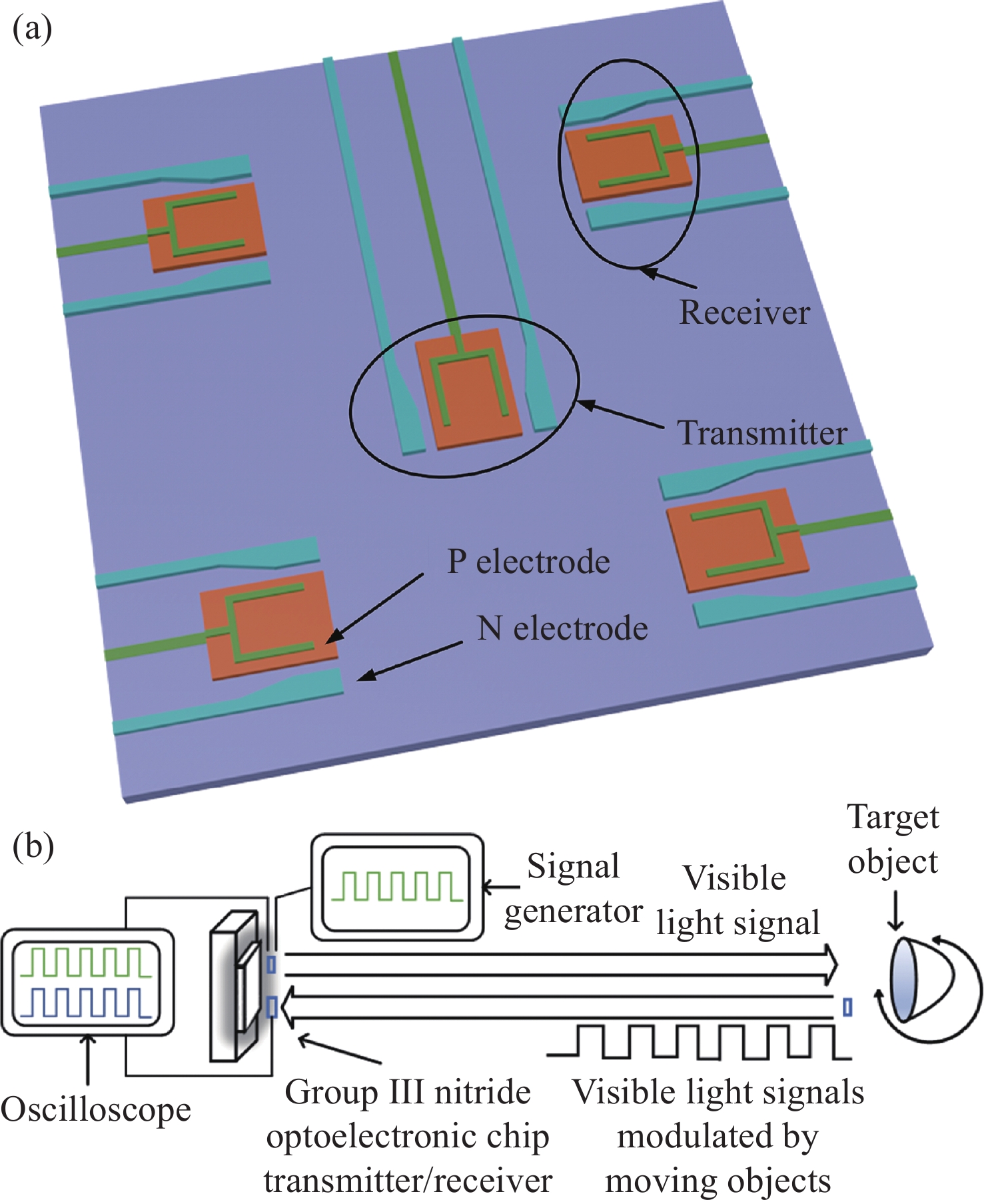
图 2 (a) III族氮化物光电子芯片示意图及其(b)运动探测系统示意图
Figure 2. (a) Schematic diagram of III-nitride optoelectronic chip and its (b) schematic diagram of motion detection system
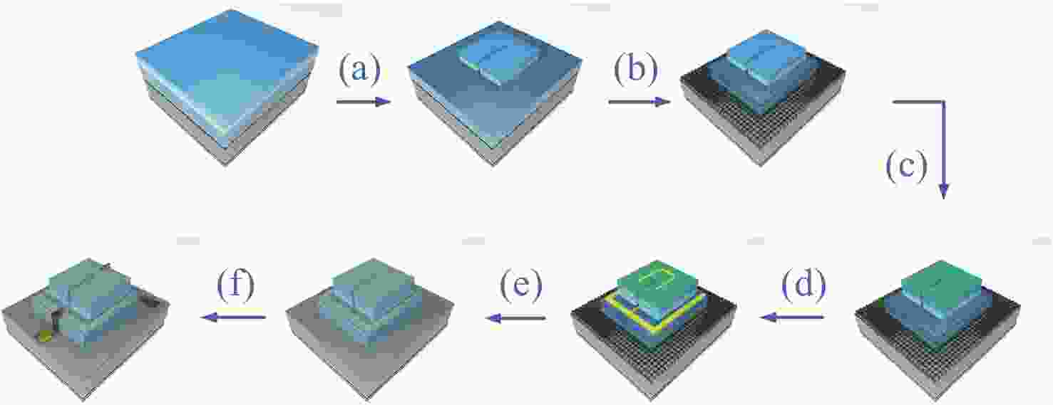
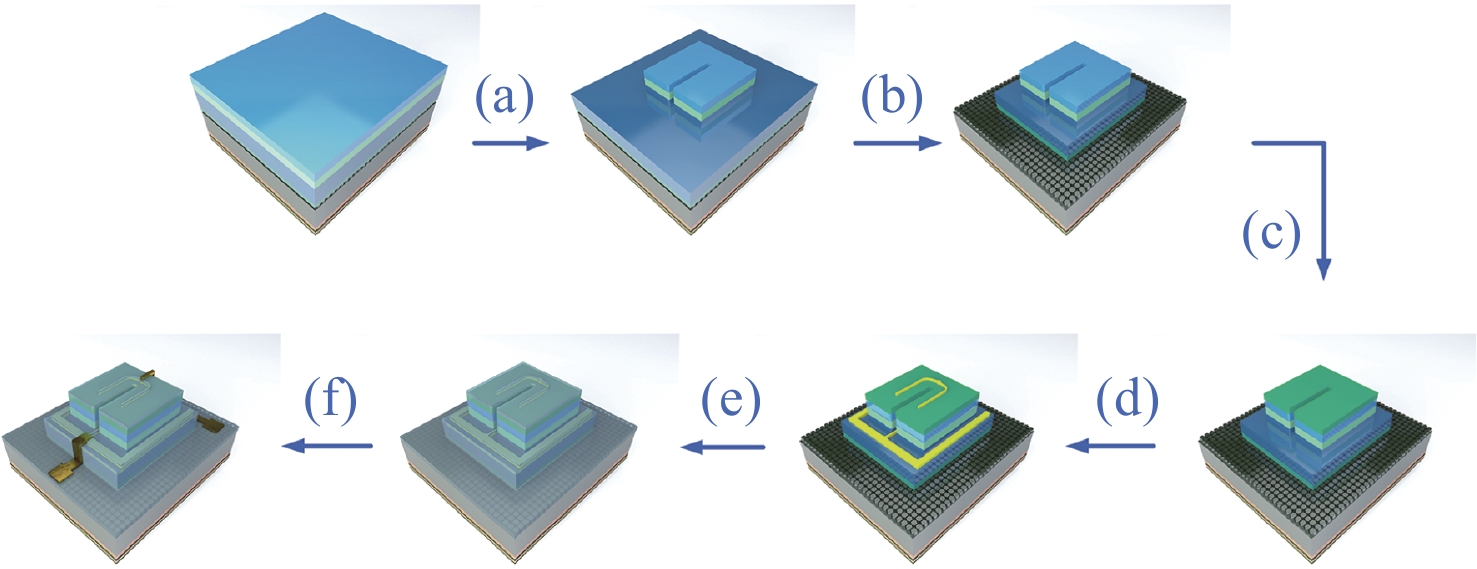
图 3 III族氮化物光电子芯片的加工流程图
Figure 3. Fabrication process of III-nitride optoelectronic chip
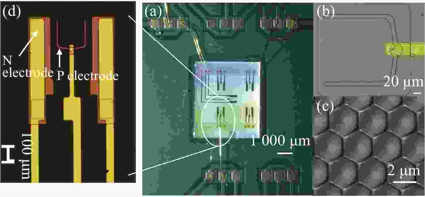
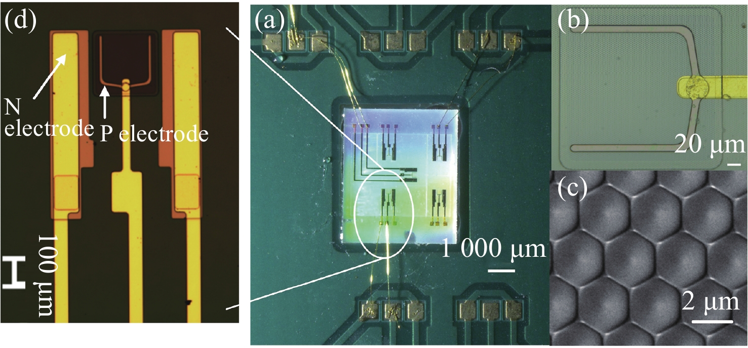
图 4 光电子芯片形貌图。(a)光电子芯片的整体光镜图;(b)发射/接收区域光镜图;(c) DBR层电子显微镜图;(d)单个发射器/接收器的局部放大光镜图
Figure 4. Morphological images of optoelectronic chip. (a) Overall optical microscope image of optoelectronic chip; (b) optical microscope image of transmitting/receiving region; (c) SEM image of DBR layer; (d) enlarged optical microscope image of a single transmitter/receiver
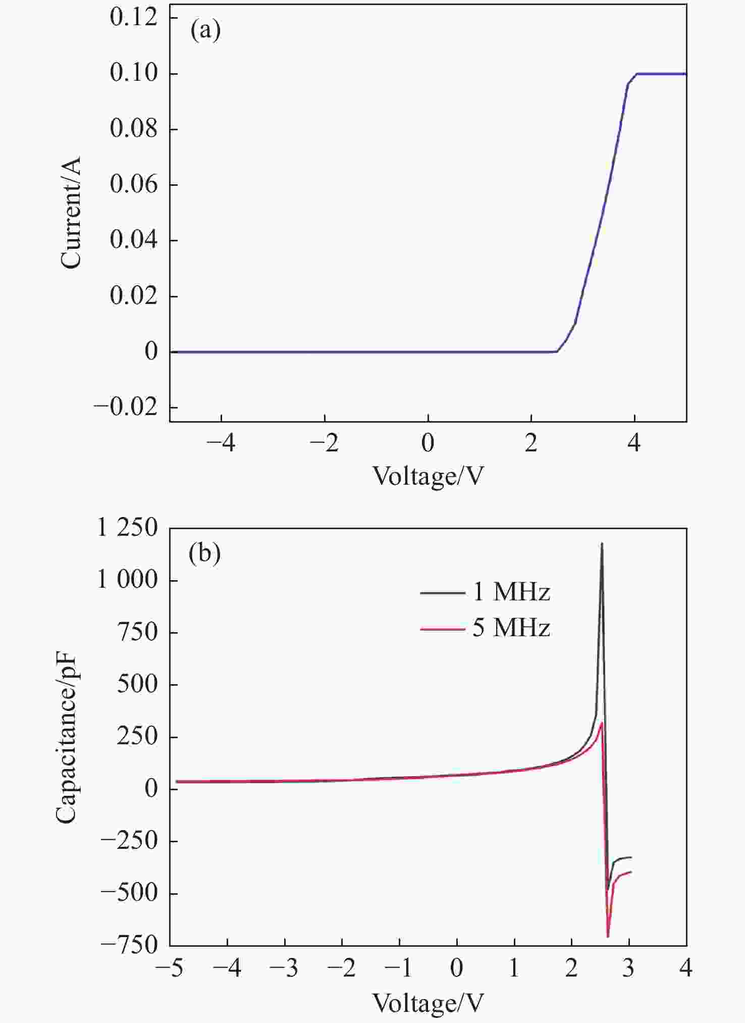
图 5 光电芯片电性能测试结果。(a)发射器/接收器的电流-电压(I-V)曲线;(b)电容-电压(C-V)曲线
Figure 5. Electrical characteristics test results. (a) Current-voltage curve of transmitter/receiver; (b) capacitance-voltage curve of transmitter/receiver
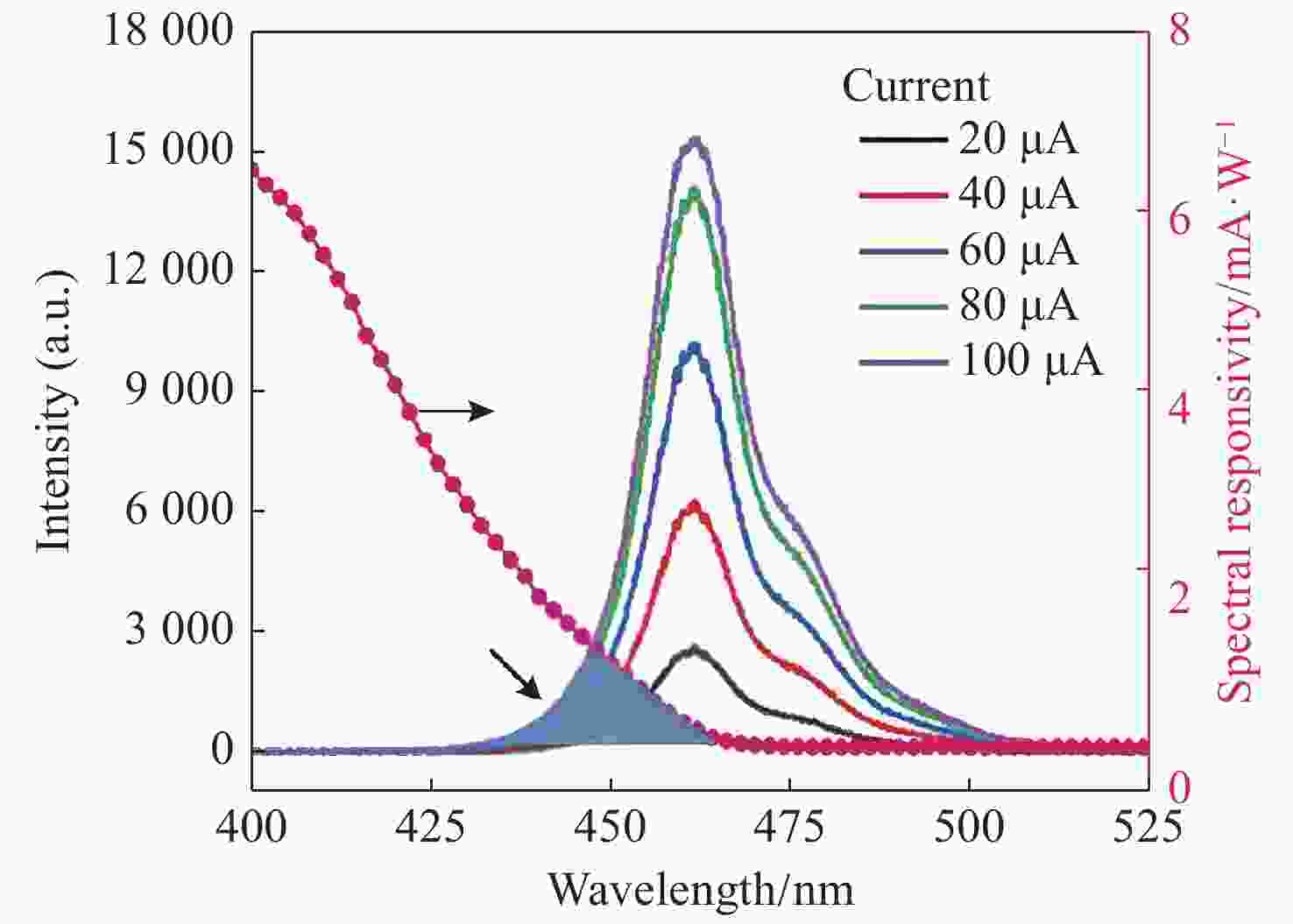
图 6 光电子芯片发射器的电致发光(EL)谱和接收器的探测谱
Figure 6. Electroluminescence (EL) spectrum of transmitter and spectral responsivity of receiver
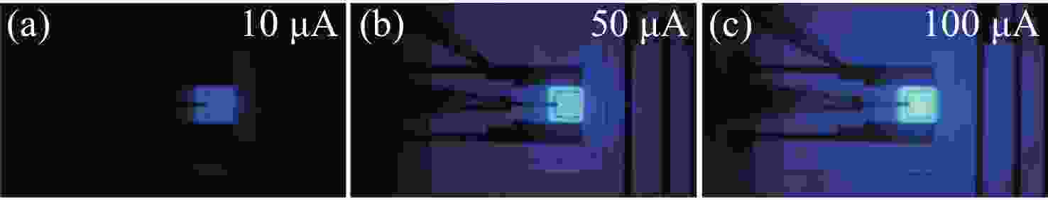
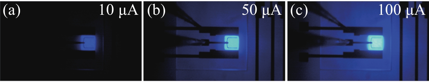
图 7 注入不同电流的发射器发光图片
Figure 7. Luminescence photographs of transmitter with different injected currents
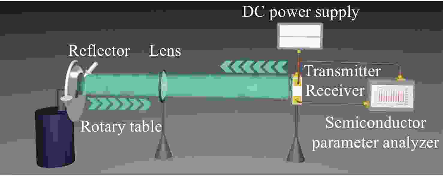
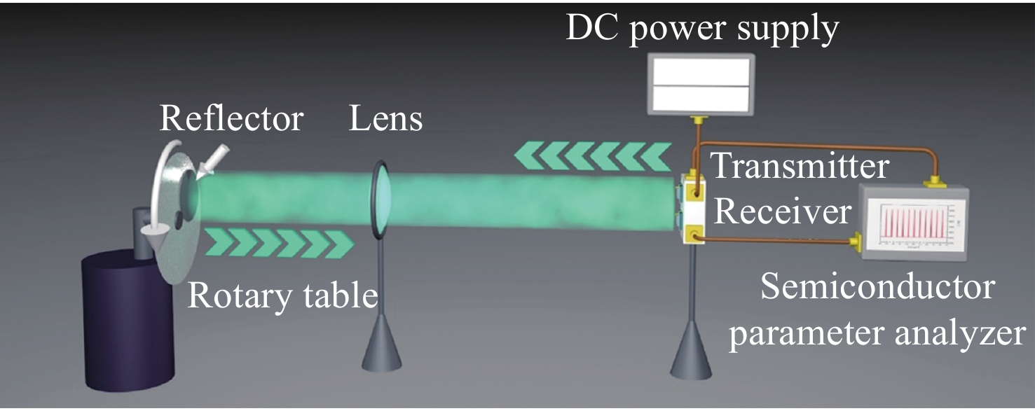
图 8 光电子芯片的运动探测系统示意图
Figure 8. Schematic diagram of motion detection system of optoelectronic chip
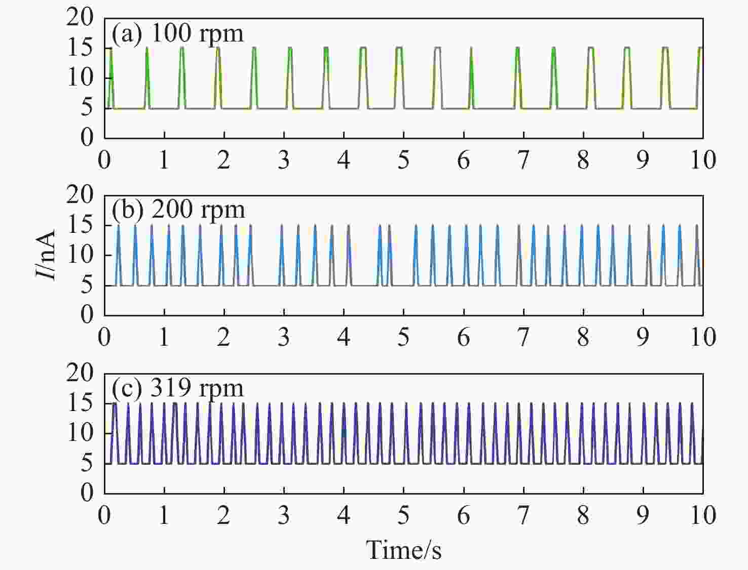
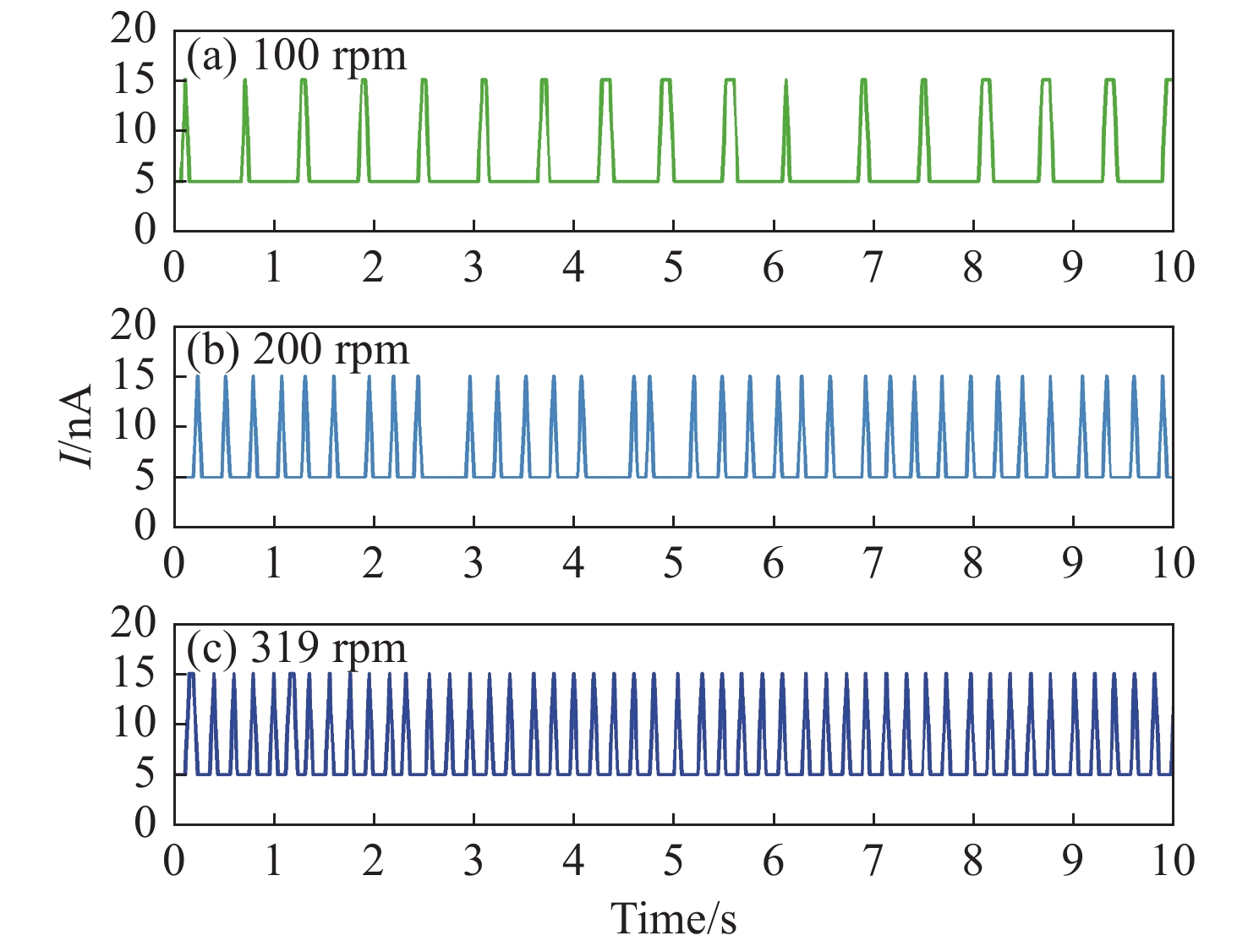
图 9 发射器偏压为2.9 V时,不同转速反射镜运动下接受器的探测光电流
Figure 9. Detected photocurrent of the receiver from the reflector moving at different rotating speeds when the transmitter is applied 2.9 V bias voltage
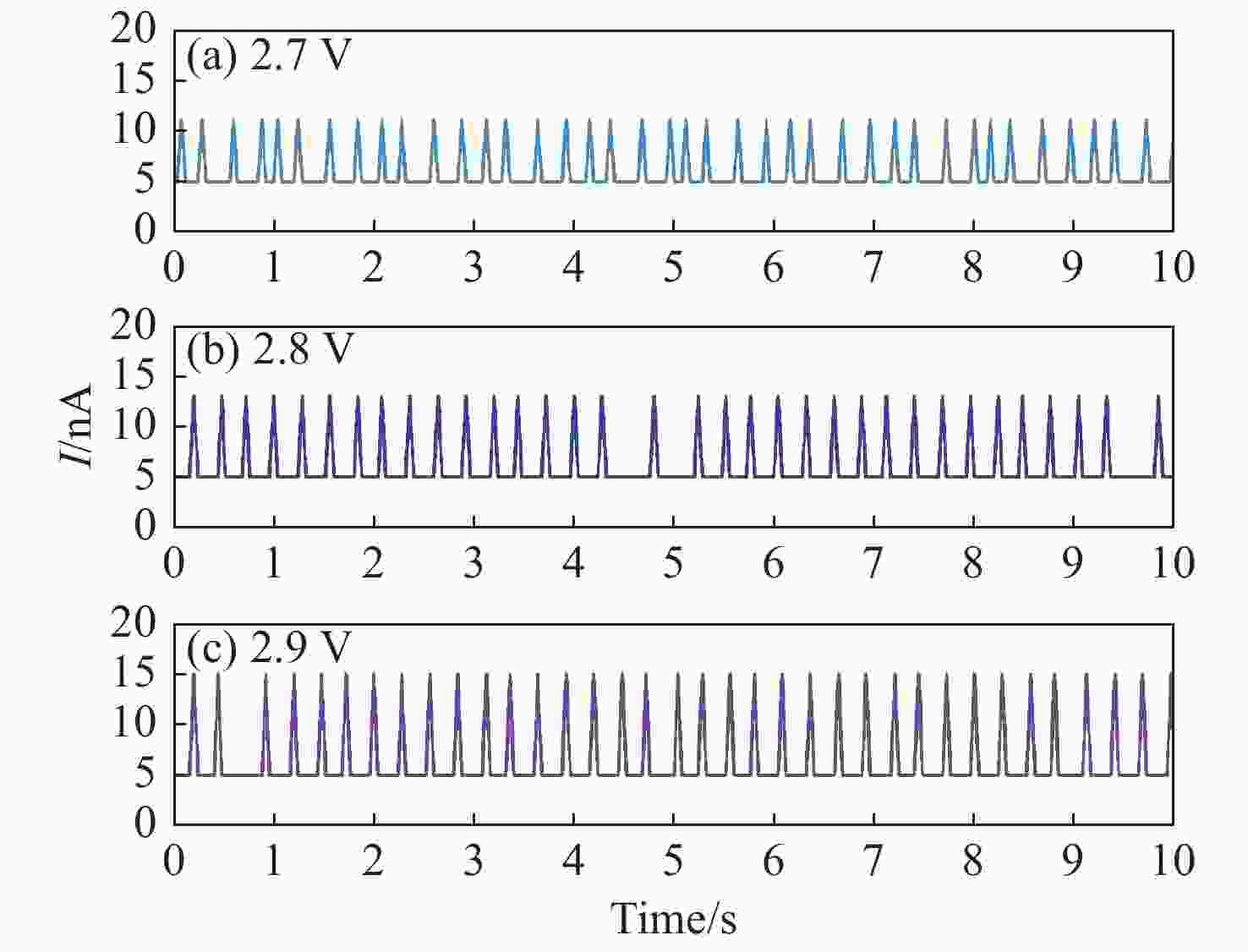
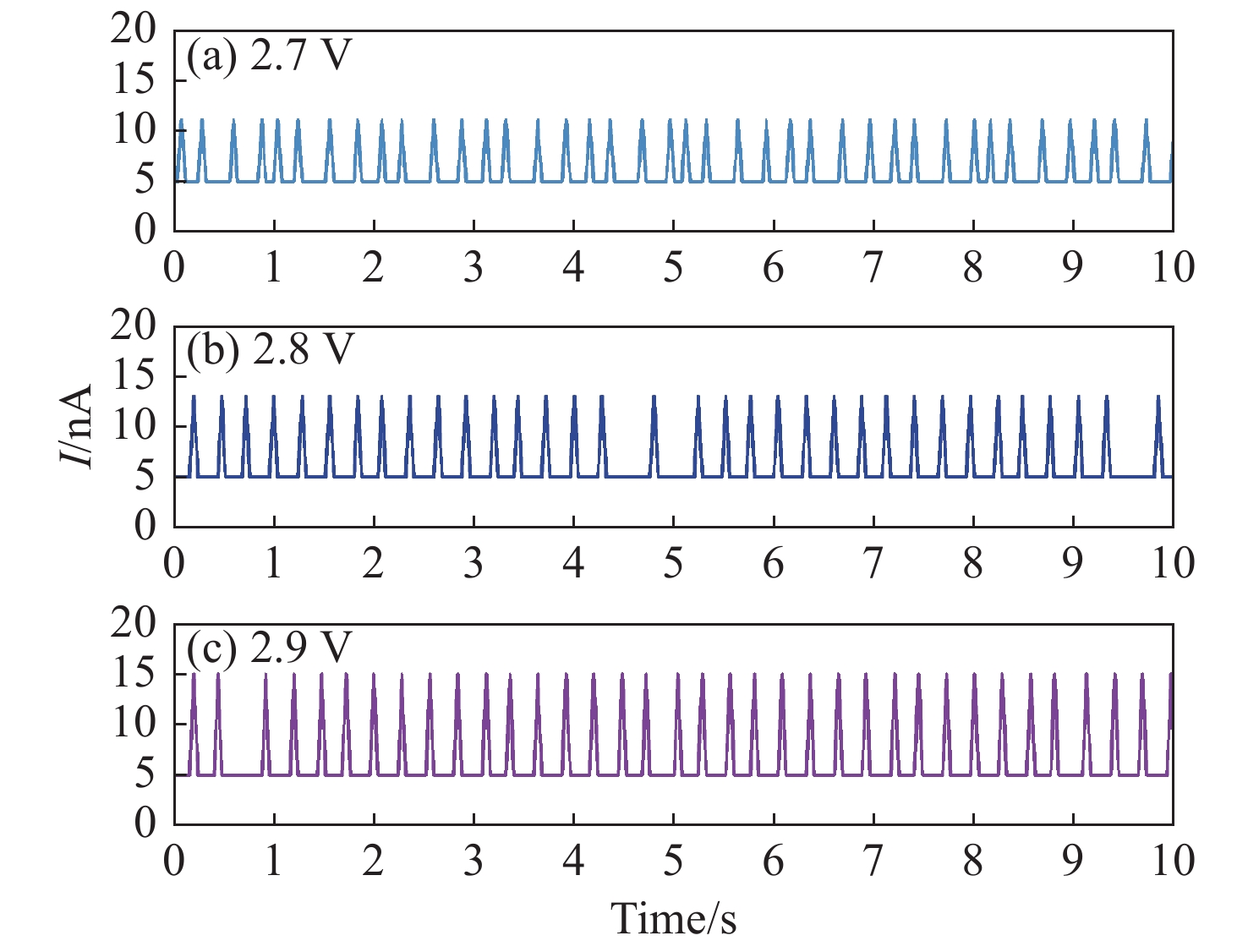
图 10 反射镜的运动转速为200 rpm,发射器偏压分别设置为2.7 V、2.8 V、2.9 V时接收器的探测光电流
Figure 10. Detected photocurrent of the receiver under 200 rpm, rotating speed of mirror when the bias voltages applied to the transmitter are set as 2.7 V, 2.8 V, 2.9 V
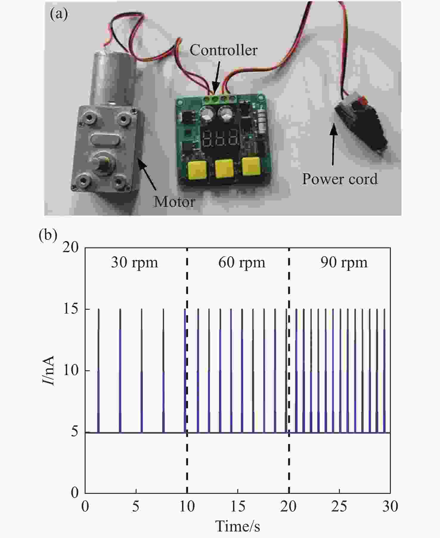
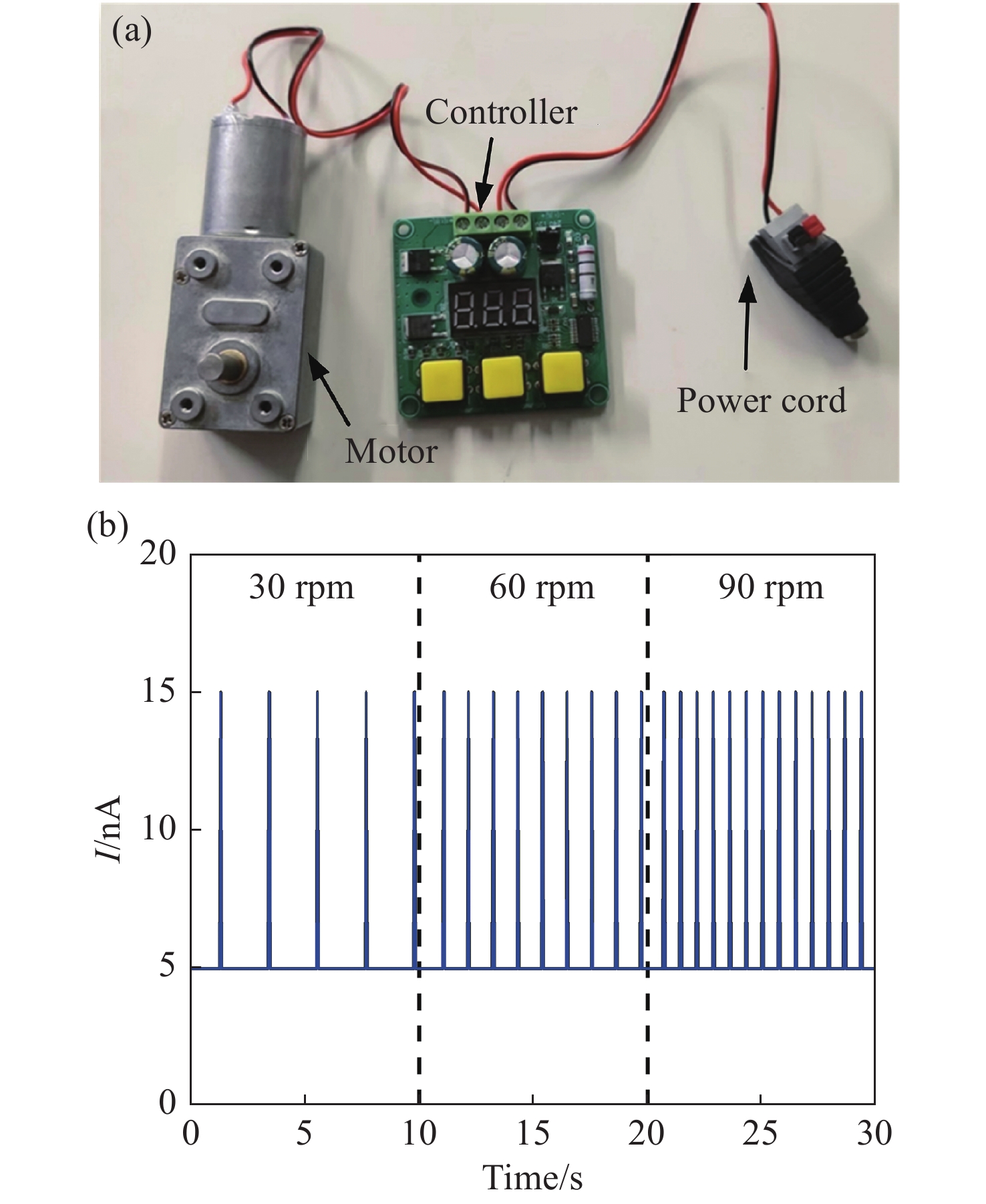
图 11 (a)变速电机和(b)变速运动探测的光电流曲线
Figure 11. (a) Variable speed motor and (b) photocurrent curve of variable speed motion detection
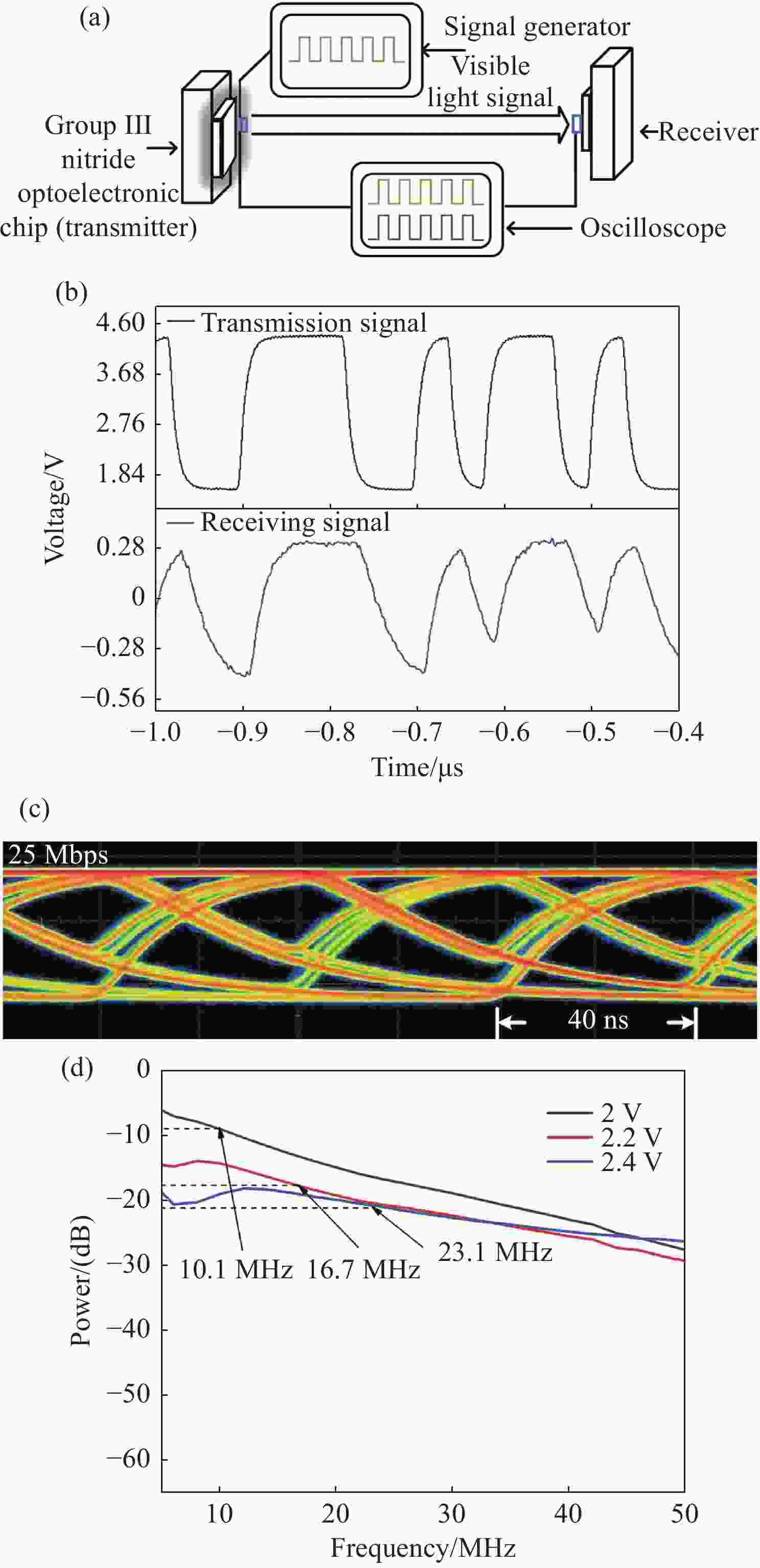
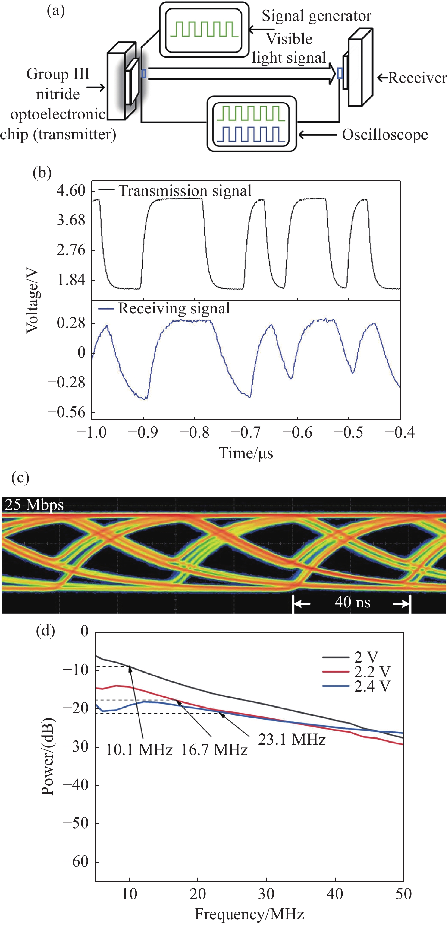
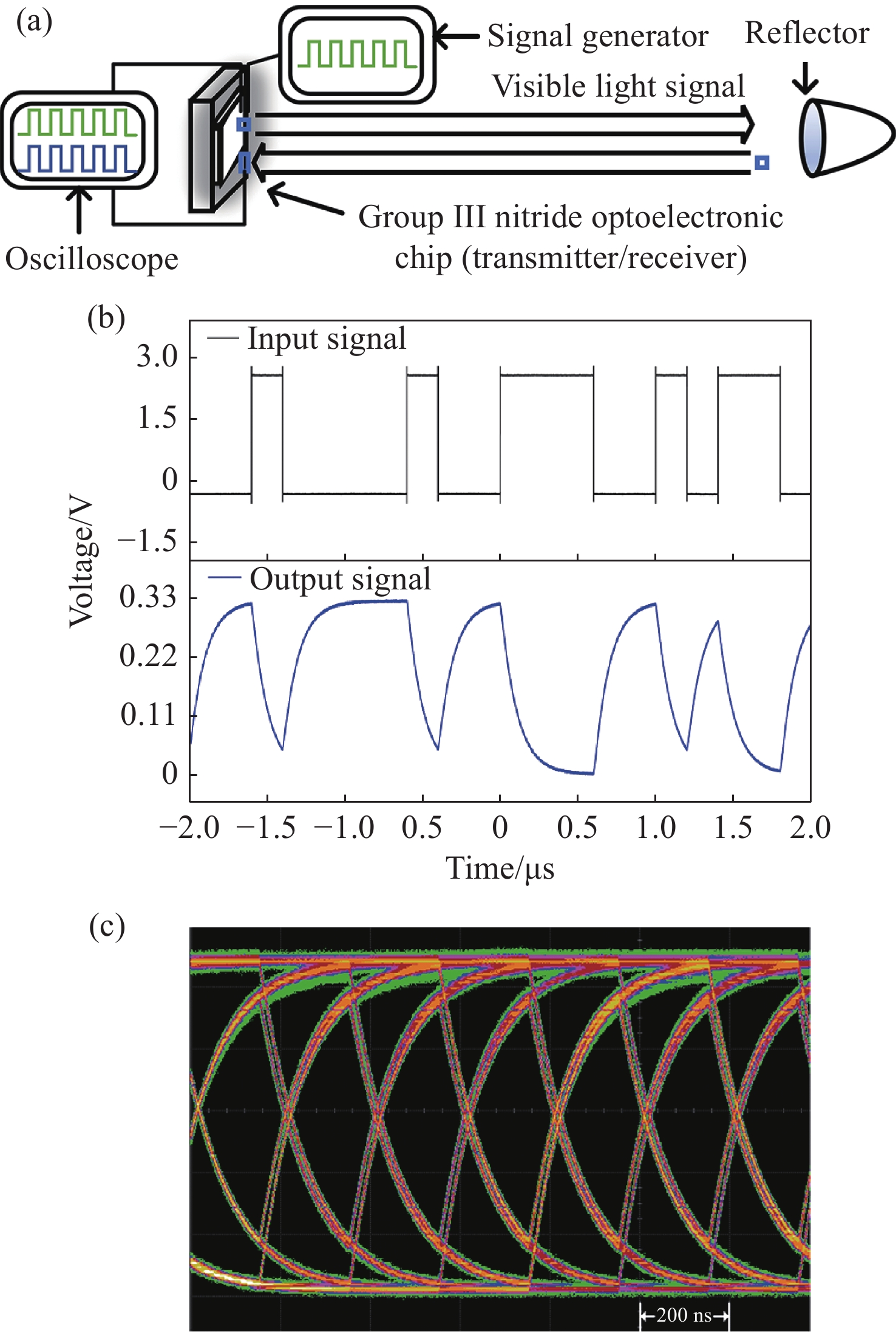
图 12 (a)作为发射器的光电子芯片的可见光通信测试系统。作为发射器的光电子芯片在25 Mbps传输速率下的收发信号波形(b)和眼图(c),以及(d)不同电压下作为发射器的光电子芯片3 dB带宽
Figure 12. (a) Visible light communication test system of optoelectronic chip as a transmitter. Signal waveforms (b) and eye diagram (c) of optoelectronic chip as a transmitter at 25 Mbps. (d) 3 dB bandwidth of optoelectronic chip as a transmitter at different bias voltages
-
[1] SCHWEIKER M, AMPATZ E, ANDARGIE M S, et al. Review of multi-domain approaches to indoor environmental perception and behaviour[J]. Building and Environment, 2020, 176: 106804. doi: 10.1016/j.buildenv.2020.106804 [2] CHEN X L, HU SH M, SUN L F. Towards real world perception and interaction[J]. Scientia Sinica Informationis, 2016, 46(8): 969-981. doi: 10.1360/N112016-00072 [3] LI A W, SHAN T Q, GUO Q, et al. Research progress of optical fiber Fabry-Perot interferometer high temperature sensors[J]. Chinese Optics, 2022, 15(4): 609-624. [4] ZHANG SH, ZHU W B, LI J, et al. Design of micro-optical system for laser displacement sensor sensing probe[J]. Chinese Optics, 2018, 11(6): 1001-1010. doi: 10.3788/co.20181106.1001 [5] SASI G. Motion detection using passive infrared sensor using IoT[J]. Journal of Physics:Conference Series, 2021, 1717: 012067. doi: 10.1088/1742-6596/1717/1/012067 [6] SINGH P, CHAULYA S K, SINGH V K, et al. Motion detection and tracking using microwave sensor for eliminating illegal mine activities[C]. 2018 3rd International Conference on Microwave and Photonics (ICMAP), IEEE, 2018: 1-5. [7] HE J, HUANG ZH, YU K. High-accuracy scheme based on a look-up table for motion detection in an optical camera communication system[J]. Optics Express, 2020, 28(7): 10270-10279. doi: 10.1364/OE.389107 [8] PARK S T, LEE J G. Improved Kalman filter design for three-dimensional radar tracking[J]. IEEE Transactions on Aerospace and Electronic Systems, 2001, 37(2): 727-739. doi: 10.1109/7.937485 [9] ACKERMANN F. Airborne laser scanning—present status and future expectations[J]. ISPRS Journal of Photogrammetry and Remote Sensing, 1999, 54(2-3): 64-67. doi: 10.1016/S0924-2716(99)00009-X [10] 邓绮雯. 免成像快速运动物体探测与三维追踪[D]. 广州: 暨南大学, 2021.DENG Q W. Imaging-free fast-moving object detection and 3-D tracking[D]. Guangzhou: Jinan University, 2021. (in Chinese) [11] FILATOV A, RYKOV A, MURASHKIN V. Any motion detector: learning class-agnostic scene dynamics from a sequence of LiDAR point clouds[C]. 2020 IEEE International Conference on Robotics and Automation (ICRA), IEEE, 2020: 9498-9504. [12] ABUELLA H, MIRAMIRKHANI F, EKIN S, et al. ViLDAR—visible light sensing-based speed estimation using vehicle headlamps[J]. IEEE Transactions on Vehicular Technology, 2019, 68(11): 10406-10417. doi: 10.1109/TVT.2019.2941705 [13] SEWAIWAR A, TIWARI S V, CHUNG Y H. Visible light communication based motion detection[J]. Optics Express, 2015, 23(14): 18769-18776. doi: 10.1364/OE.23.018769 [14] SAWAKI N, HONDA Y. Semi-polar GaN LEDs on Si substrate[J]. Science China Technological Sciences, 2011, 54(1): 38-41. doi: 10.1007/s11431-010-4182-2 [15] LI D B, JIANG K, SUN X J, et al. AlGaN photonics: recent advances in materials and ultraviolet devices[J]. Advances in Optics and Photonics, 2018, 10(1): 43-110. doi: 10.1364/AOP.10.000043 [16] CHEN L, WU Y P, LI K H. Monolithic InGaN/GaN photonic chips for heart pulse monitoring[J]. Optics Letters, 2020, 45(18): 4992-4995. doi: 10.1364/OL.400733 [17] YU H M, SUN A F, LIU Y Q, et al. Capacitive sensor based on GaN honeycomb nanonetwork for ultrafast and low temperature hydrogen gas detection[J]. Sensors and Actuators B:Chemical, 2021, 346: 130488. doi: 10.1016/j.snb.2021.130488 [18] ZHANG SH, SHI ZH, YUAN J L, et al. Membrane light-emitting diode flow sensor[J]. Advanced Materials Technologies, 2018, 3(3): 1700285. doi: 10.1002/admt.201700285 [19] WANG Y J, YIN Q X, YE Z Q, et al. Chip and its key technology for monolithically integrated visible light communication and sensing[J]. Journal of Electronics & Information Technology, 2022, 44(8): 2725-2729. doi: 10.11999/JEIT211559 -

 下载:
下载:


计量
- 文章访问数: 995
- HTML全文浏览量: 460
- PDF下载量: 209
- 被引次数: 0
