


-
摘要:
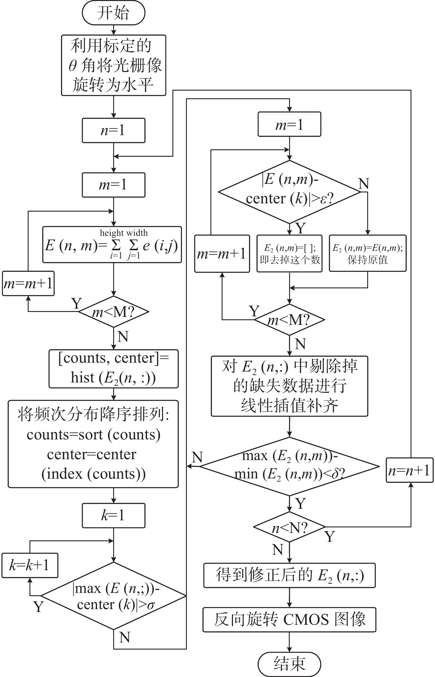
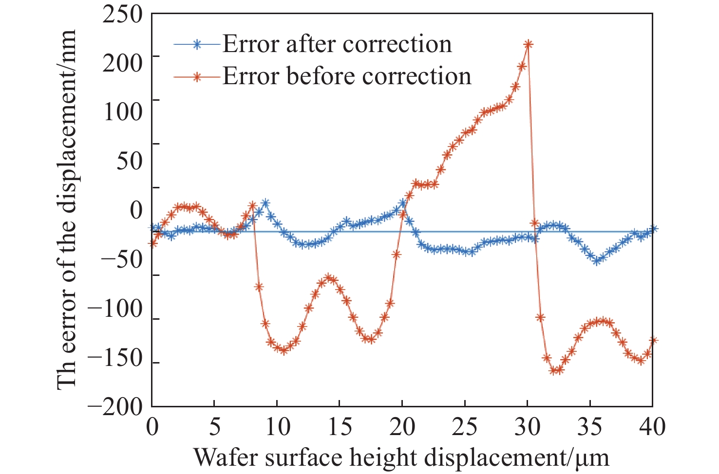
数字光栅位移测量技术将CMOS相机的像素阵列当作一个“数字化”的光栅,通过构造光学光栅像和数字光栅的周期差,利用微米级的光学光栅像,实现纳米级的位移测量。其可以应用于光刻机的调焦调平传感器中,结合倾斜入射的检测光路,对晶圆表面高度进行精确测量。在实际测量中,晶圆表面意外出现的图形会干扰光学光栅的反射成像,进而影响图像处理结果。针对上述问题,本文提出一种数字光栅位移测量的工艺适应性方法,以数字光栅周期为单位,对存在干扰图案时的CMOS图像进行光强重建和光强曲线恢复。该方法能在晶圆基底出现较大面积图案时表现出很好的稳定性,且可以适应多种表面缺陷,如划痕、颗粒、污渍和沟槽等。实验结果表明,经图像光强重建后,光强曲线的均方误差大幅减小,修正后的
Z 向测量误差在±33 nm(±3σ =±41.2 nm)以内。该方法能增强数字光栅调焦调平传感器的工艺适应性,为调焦调平方法提供技术参考。Abstract:In the digital grating displacement measurement technique, the CMOS pixel array of the camera is regarded as a ‘digitized’ grating. The micron-scale grating images can realize nanoscale displacement measurements by constructing the period difference between optical grating and digital grating. Combined with the detection light path of oblique incidence, it can be applied to the lithography machine’s focusing and leveling sensor to measure the wafer surface height accurately. In the actual measurement, the unexpected patterns on the wafer surface interfere with the reflection imaging of the optical grating, then affect the image processing results. In this paper, a process adaptability method for digital grating displacement measurement is proposed, which reconstructs the light intensity and recovers the light intensity curve from the CMOS image when interference patterns exist. The proposed method shows good stability when the large area pattern appears on the wafer substrate, and can adapt to multiple surface defects such as scratches, particles, stains and grooves. The experimental results show that the mean square error of the light intensity curve is significantly reduced and the method’s
Z -direction error correction is within ±33 nm (±3σ =±41.2 nm) after reconstructing the light intensity. This method can enhance the process adaptability of the digital grating focusing and leveling sensor. Therefore, it can serve as a technical reference for the focusing and leveling method.-
Key words:
- focusing and leveling /
- digital grating /
- displacement measurement /
- process adaptability
-
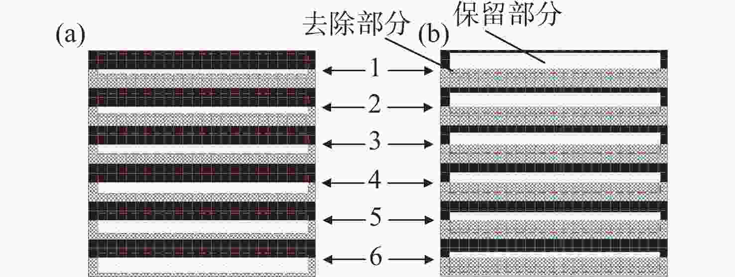
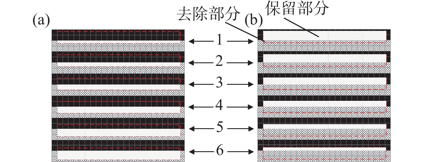
图 2 数字光栅对光学光栅像的(a)保留和(b)去除
Figure 2. (a) Preservation and (b) removal of optical grating image by digital grating
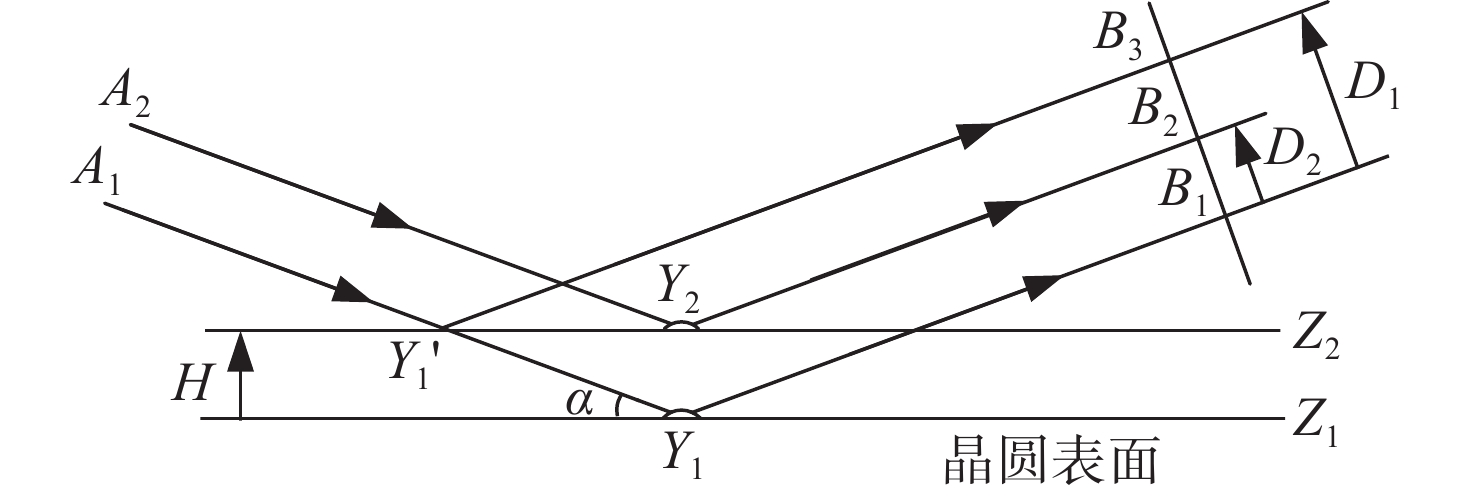
图 6 晶圆表面图案成像与光学光栅像位移不同步
Figure 6. Displacement out of sync between the wafer surface pattern imaging and the optical grating imaging
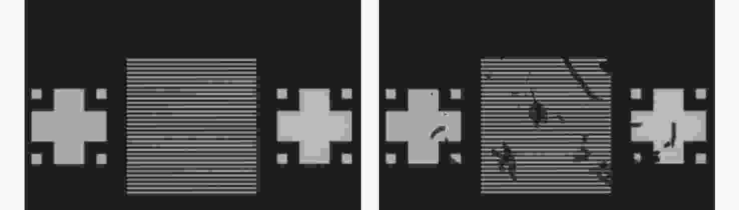
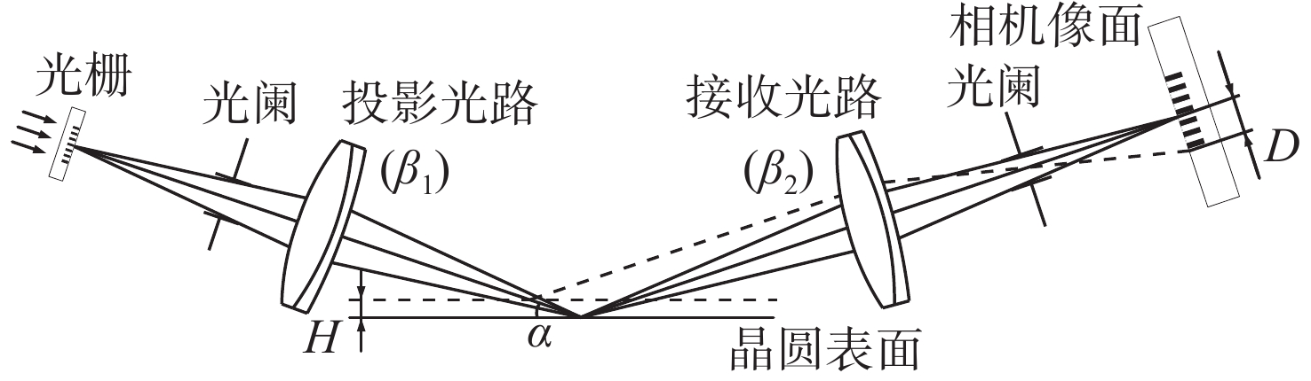
图 7 CMOS像素阵列上接收到的光学光栅像示意图
Figure 7. Schematic diagram of the optical grating image on the CMOS pixel array

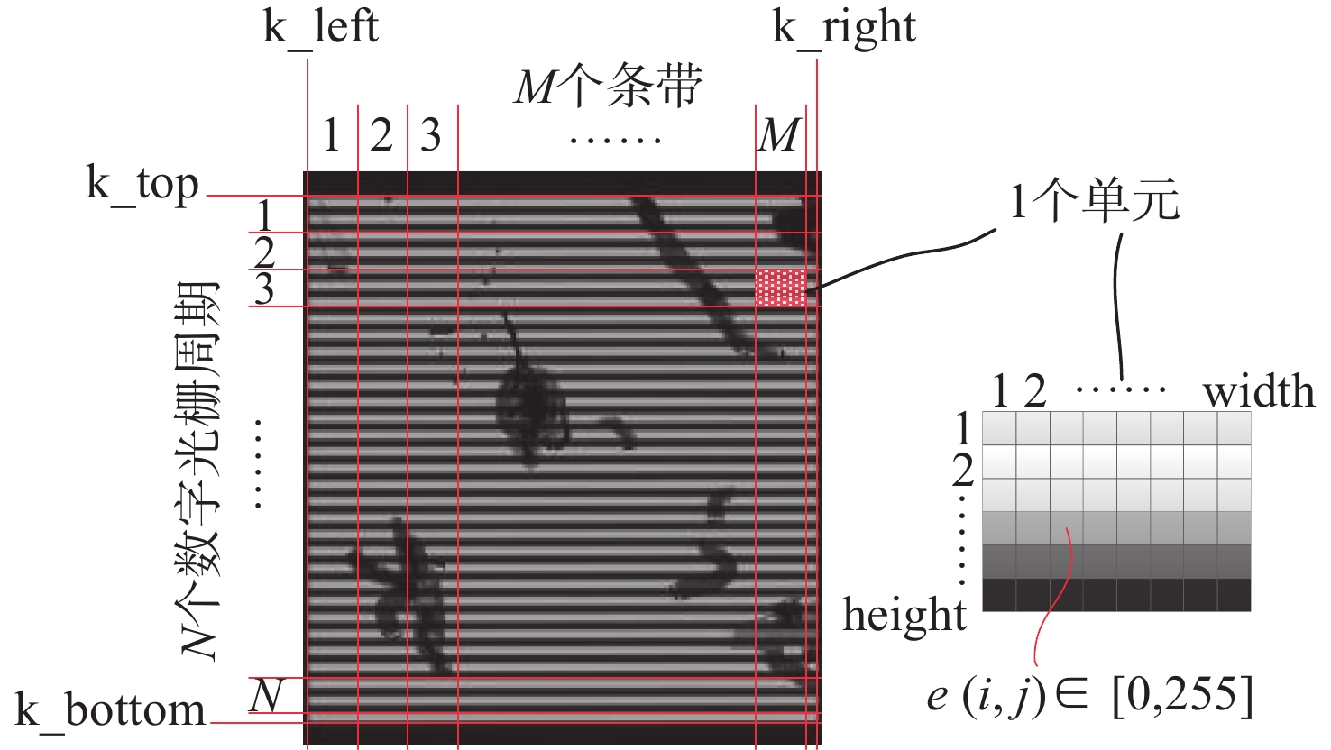
图 9 标定前的一个数字光栅周期内的累计光强
Figure 9. The accumulated light intensity in one digital grating period before calibration
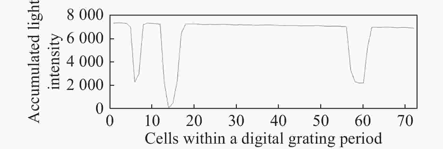
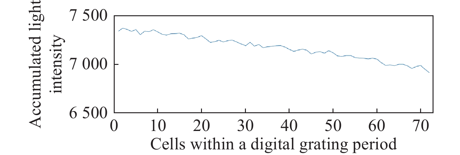
图 10 晶圆表面有图案时一个数字光栅周期内的累计光强
Figure 10. The accumulated light intensity in one digital grating period with patterns on the surface of the water
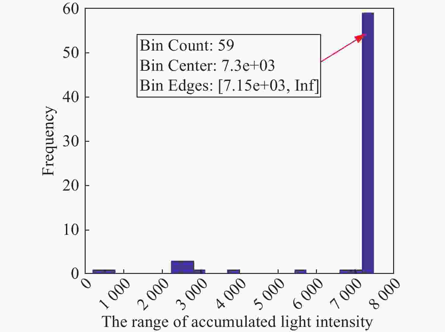
图 12 M个累计光强值的分布区间统计
Figure 12. Statistics of the distribution interval of M accumulated light intensity values
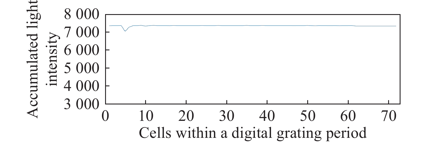
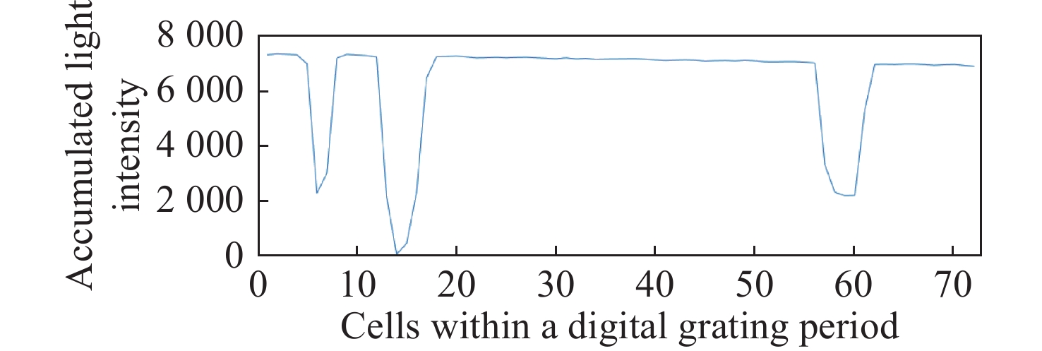
图 13 修正后的累计光强(一个数字光栅周期)
Figure 13. Corrected accumulated light intensity curve (in one digital grating period)
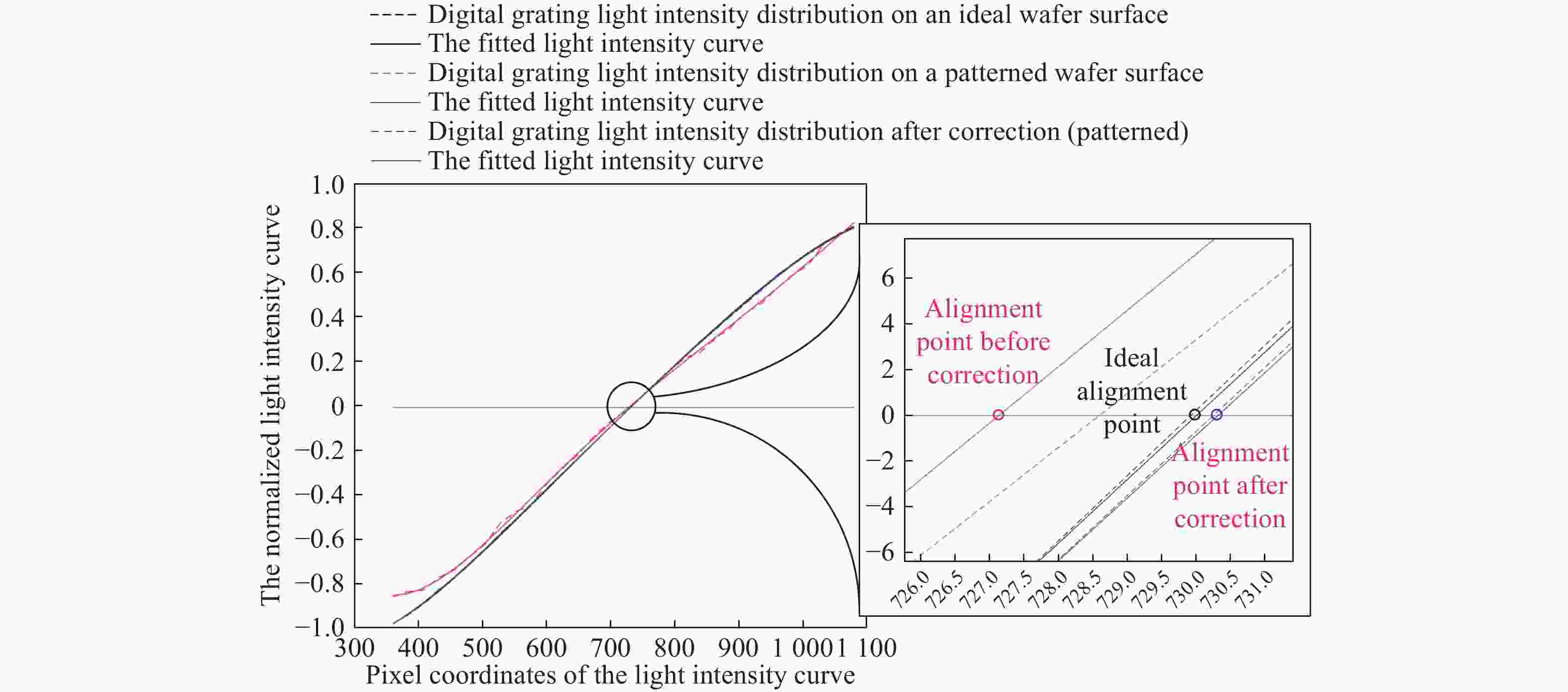
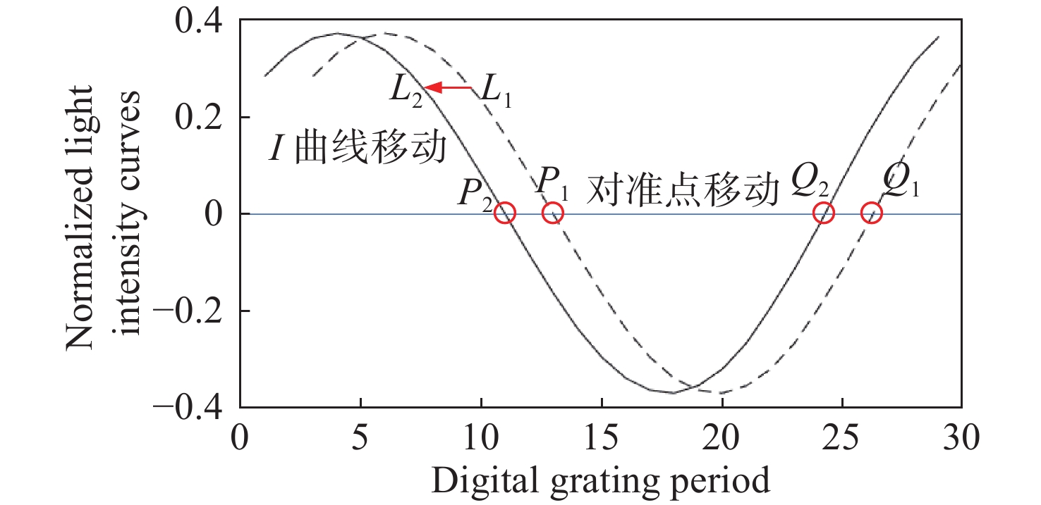
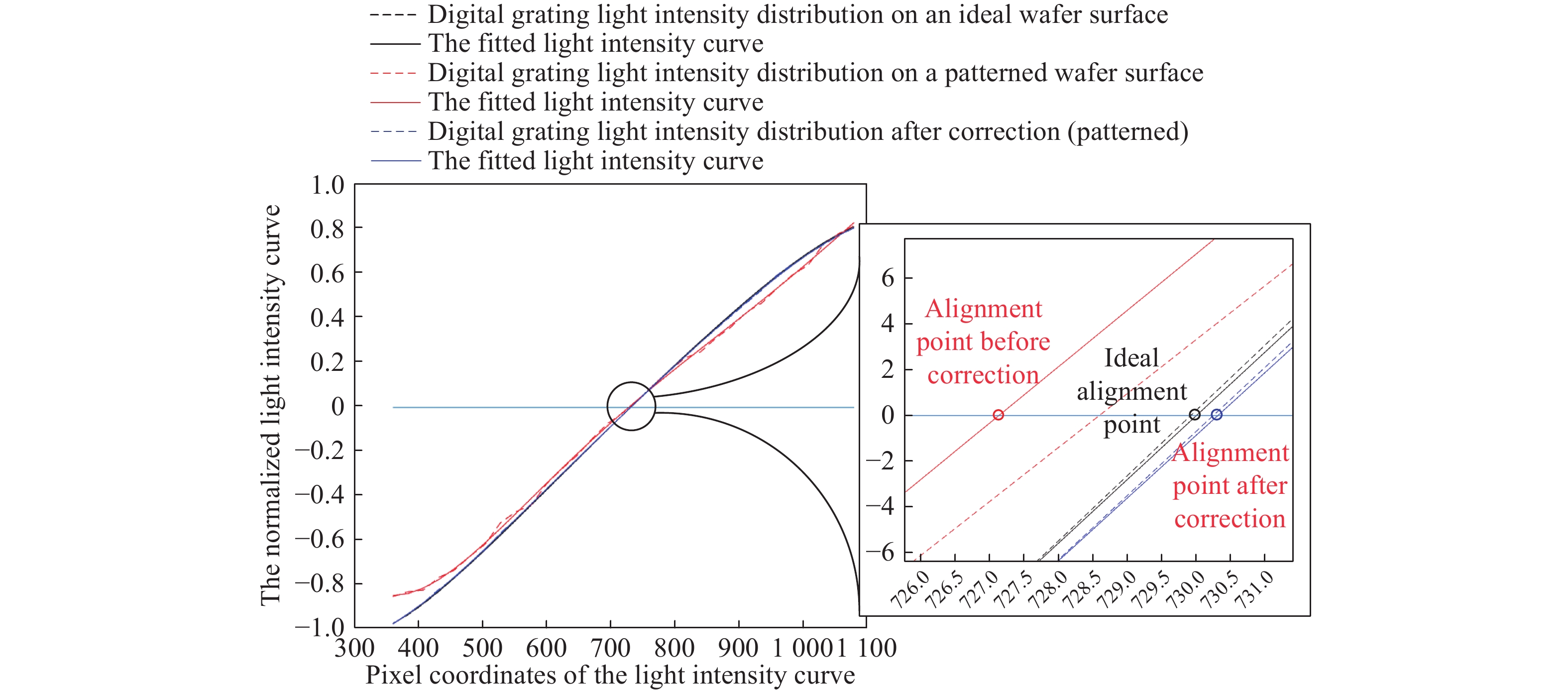
图 15 修正前后的光强曲线和对准点及其放大图
Figure 15. Light intensity curves, alignment points and their enlarged views before and after correction
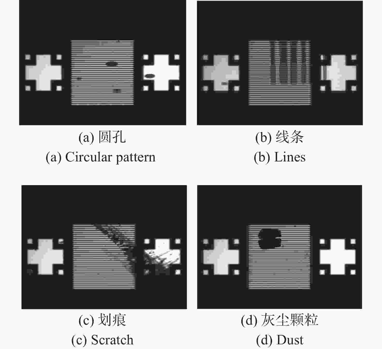
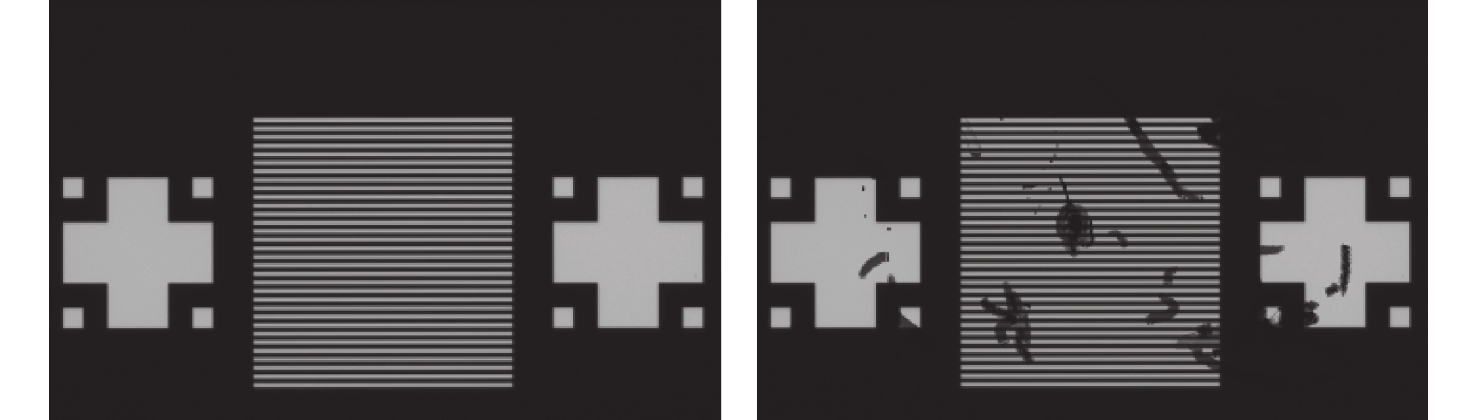
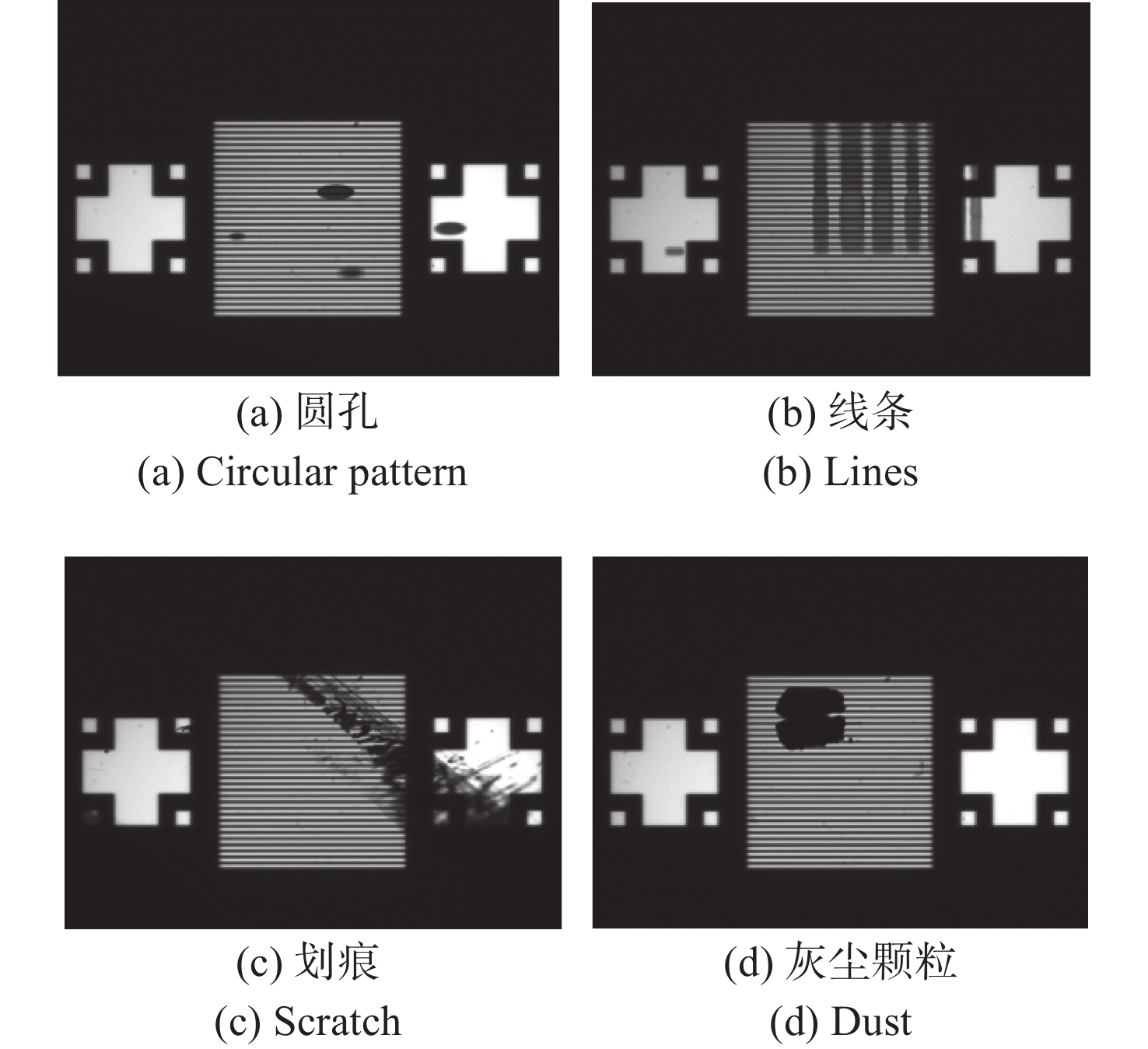
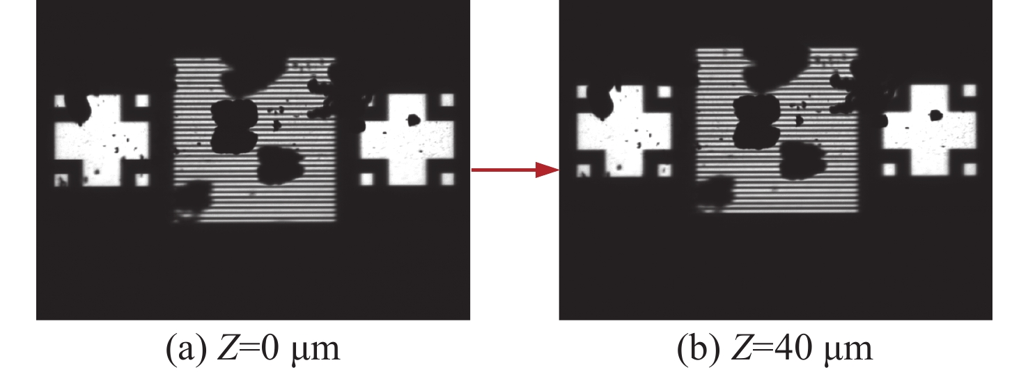
图 16 晶圆表面出现4种图案时对应的光学光栅像
Figure 16. The corresponding optical grating image when 4 patterns appear on the wafer surface
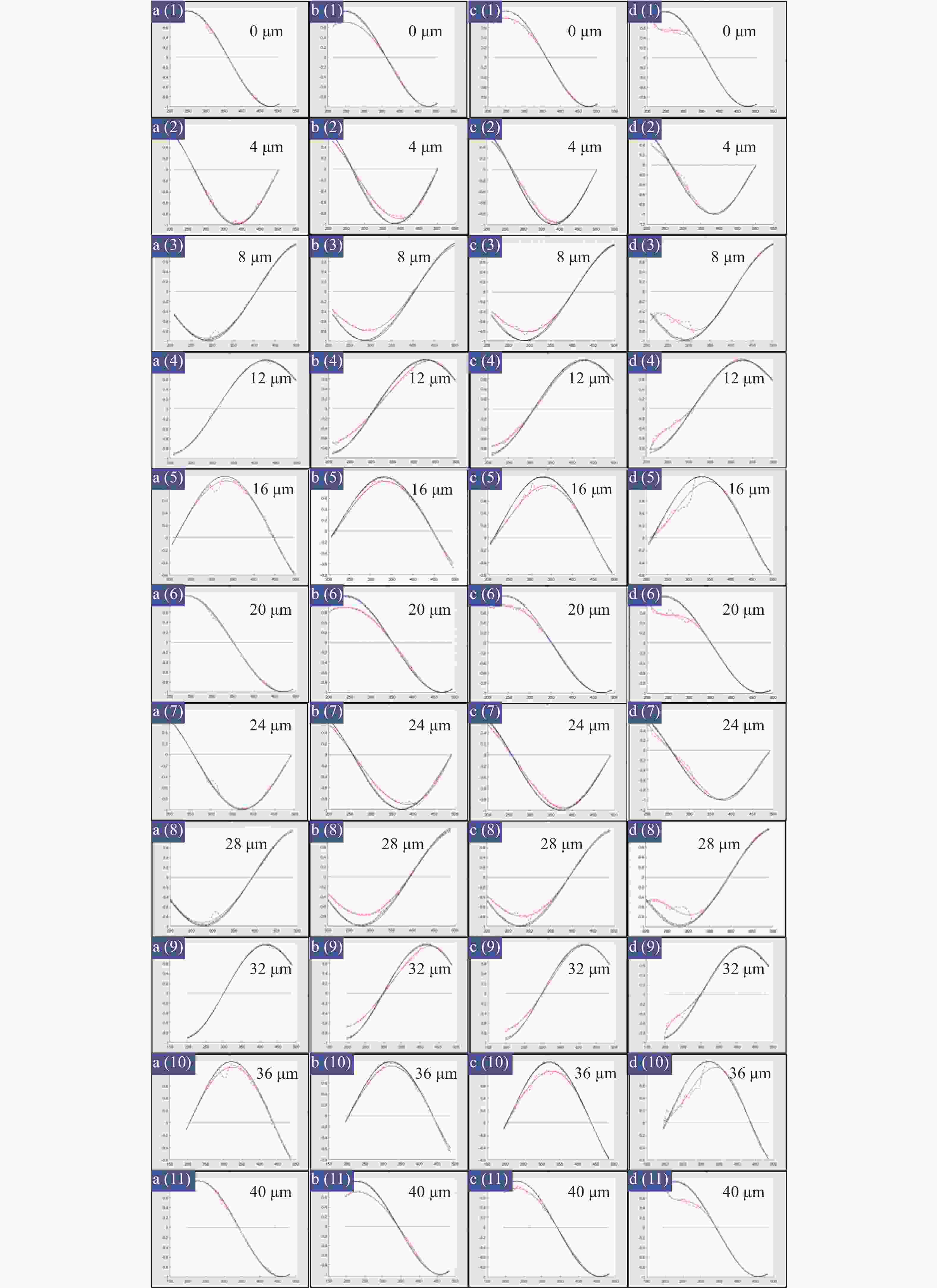
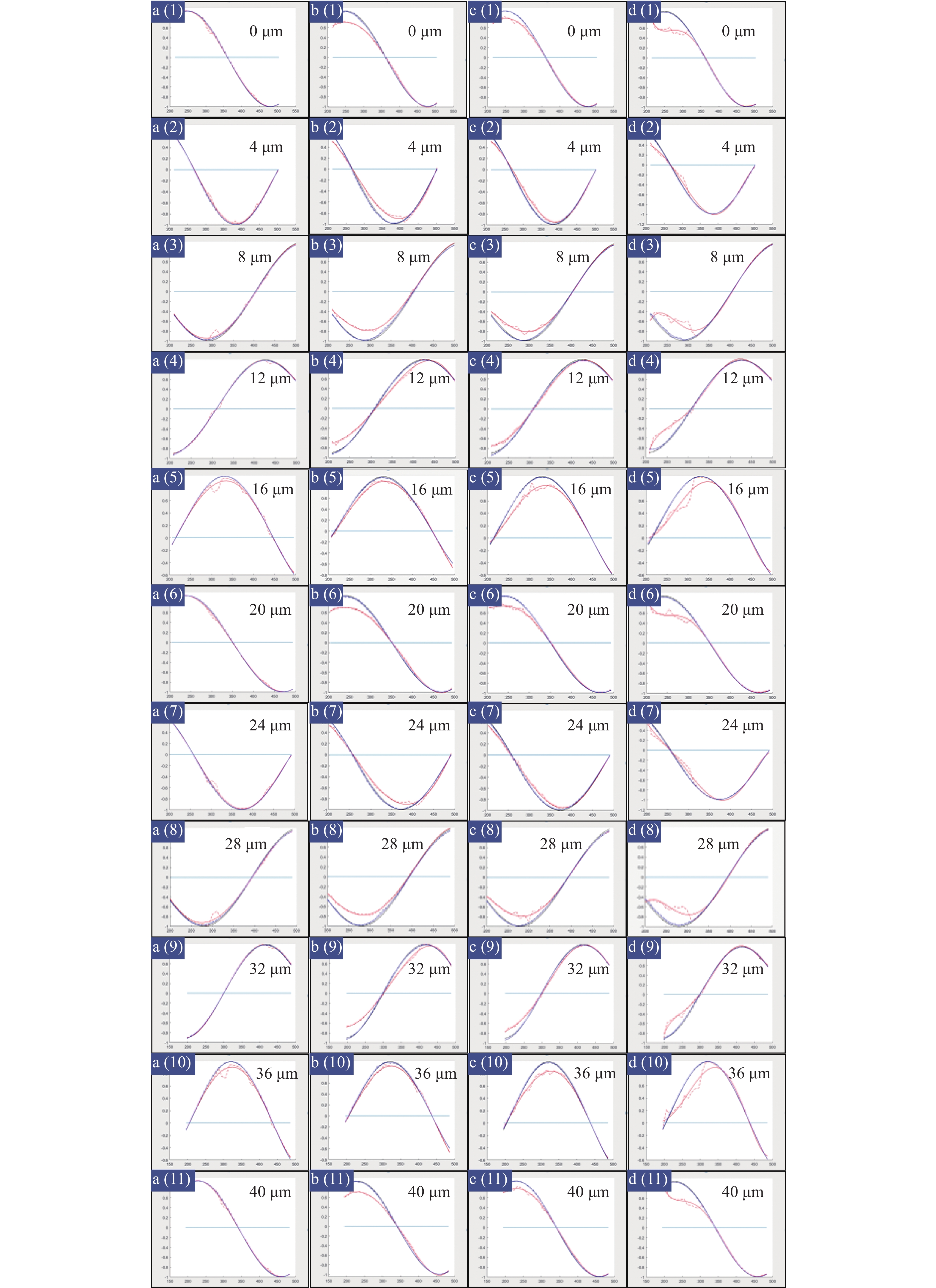
图 17 不同晶圆表面在Z轴在0 μm到40 μm不同位置对应的光强I曲线,黑色为洁净表面时对应的光强曲线,红色为表面存在图案时的光强曲线,蓝色为修正后的光强曲线(a、b、c、d分别代表圆孔、竖线、划痕和灰尘颗粒)
Figure 17. The light intensity I curves for different wafer surfaces during the Z-axis from 0 μm to 40 μm, where the black curves are the light intensity curves when the surface is clean, the red curves are for the pattern existing on the surface, and the blue ones are the corrected light intensity curves (a,b,c,d represent circular pattern, lines, scratches, and dust respectively)
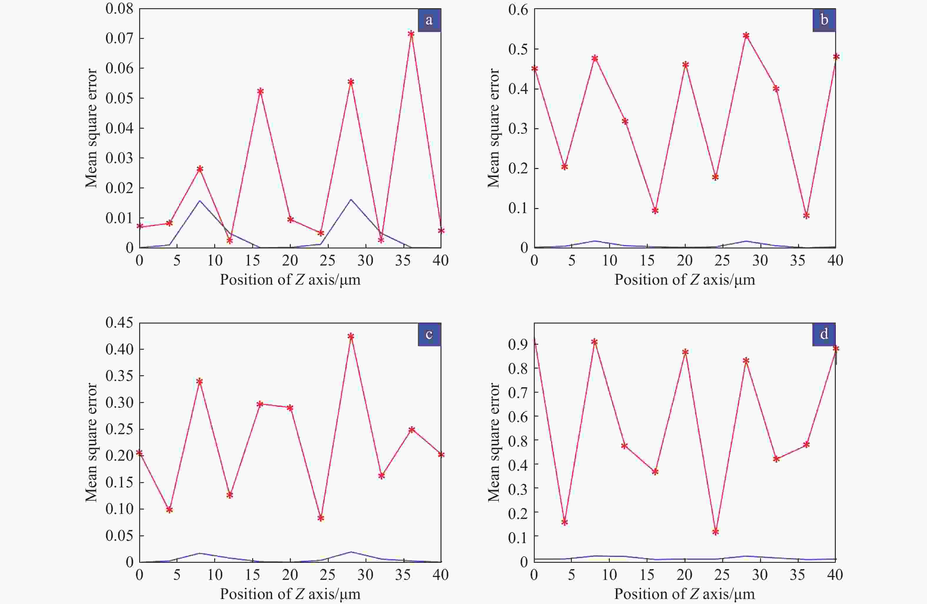
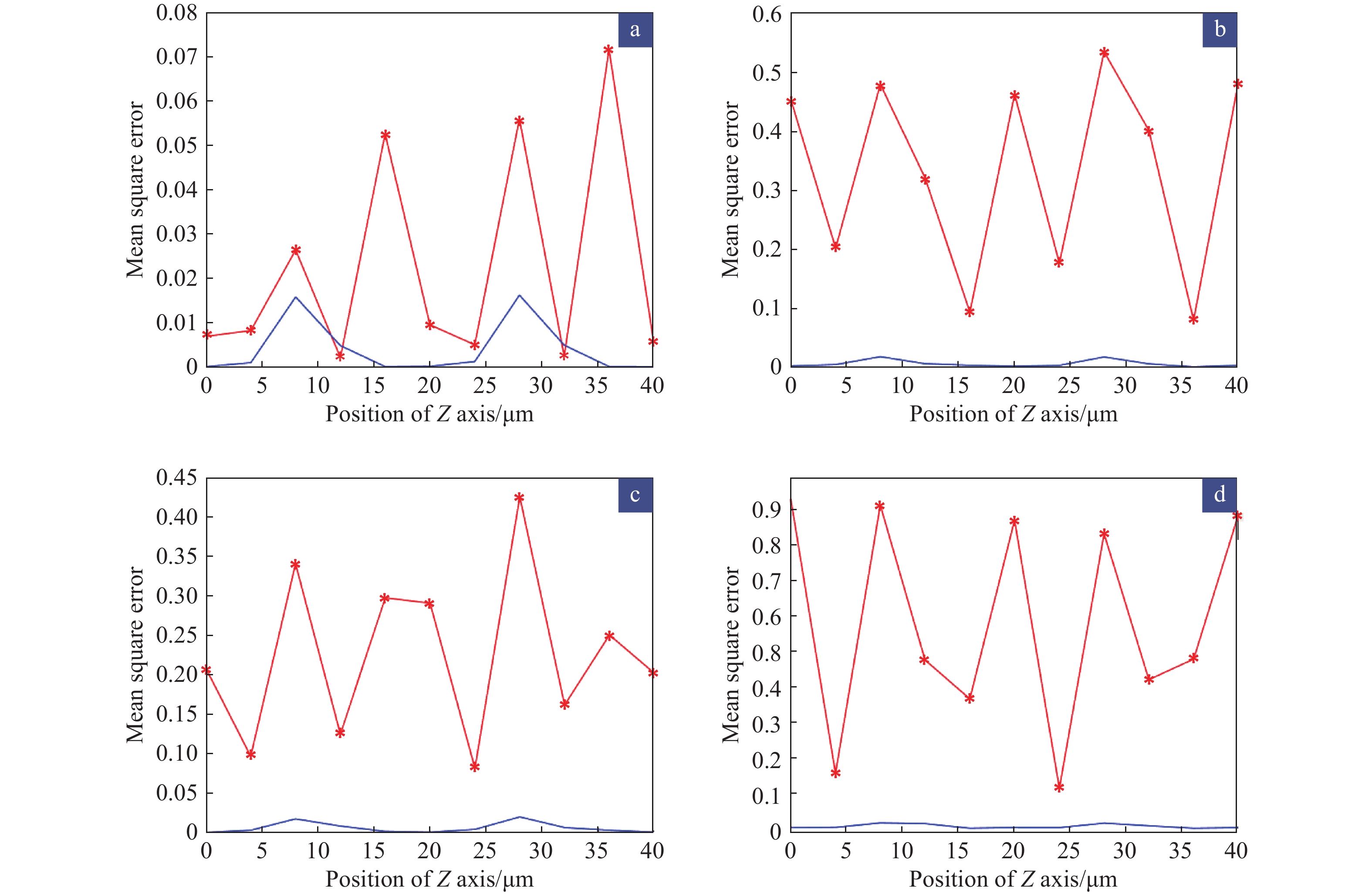
图 18 不同晶圆表面在Z轴不同位置对应的光强I曲线拟合的均方误差。(a)圆孔,(b)线条,(c)划痕,(d)颗粒
Figure 18. Mean square error of fitting corresponding intensity I curves for different wafer surfaces during Z direction stepping. (a) Circular pattern, (b) lines, (c) scratch, (d) dust

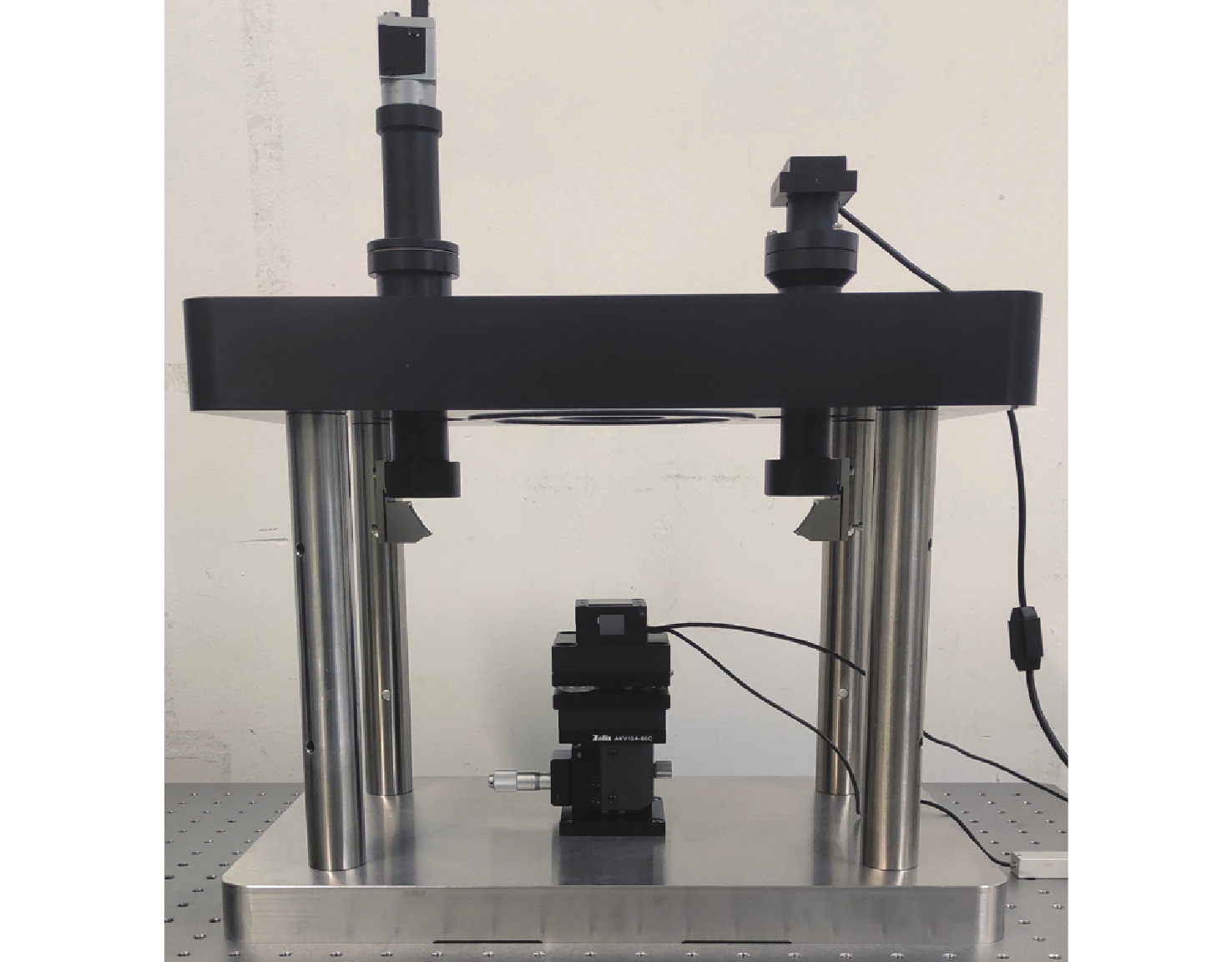
图 19 基于数字光栅的调焦调平传感器测试平台
Figure 19. Testing platform of focusing and leveling sensor based on digital grating
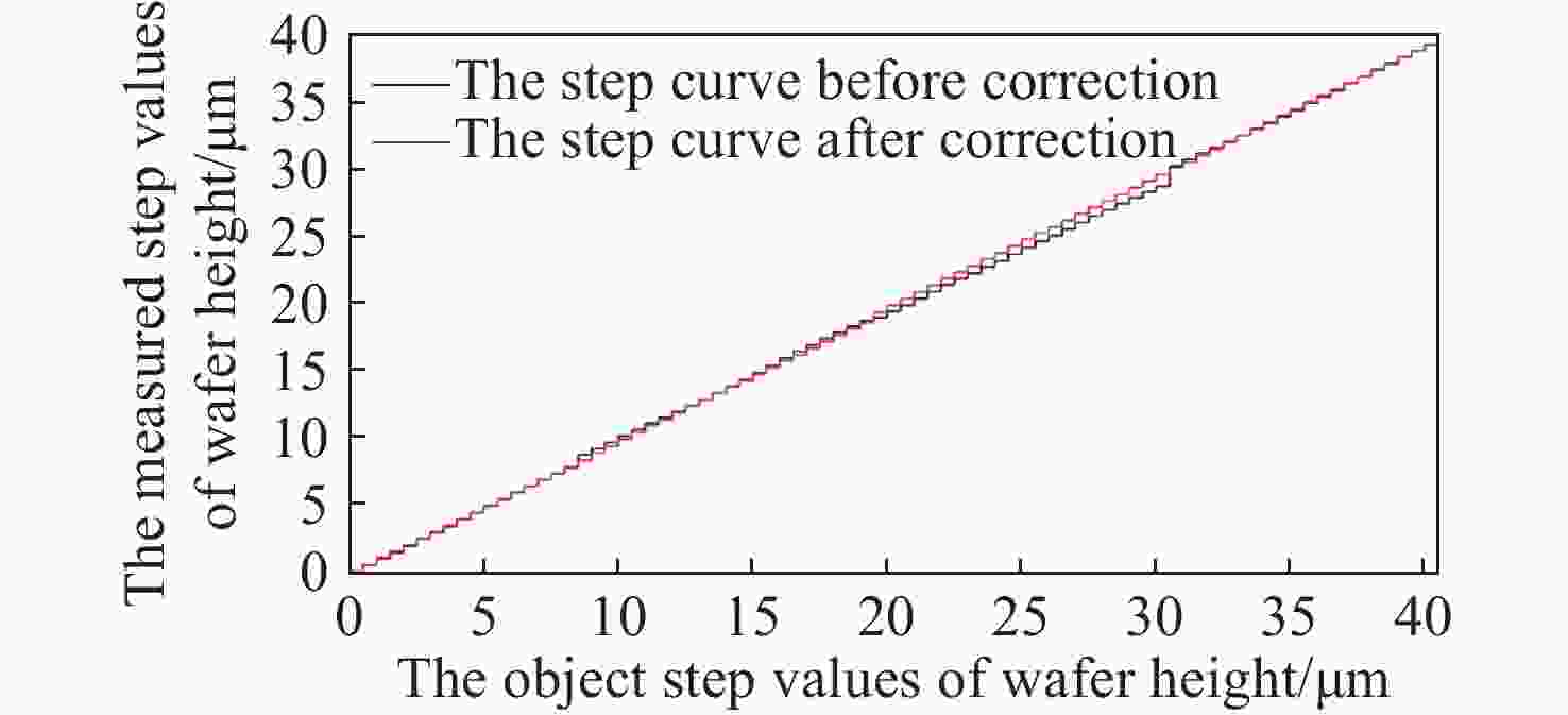
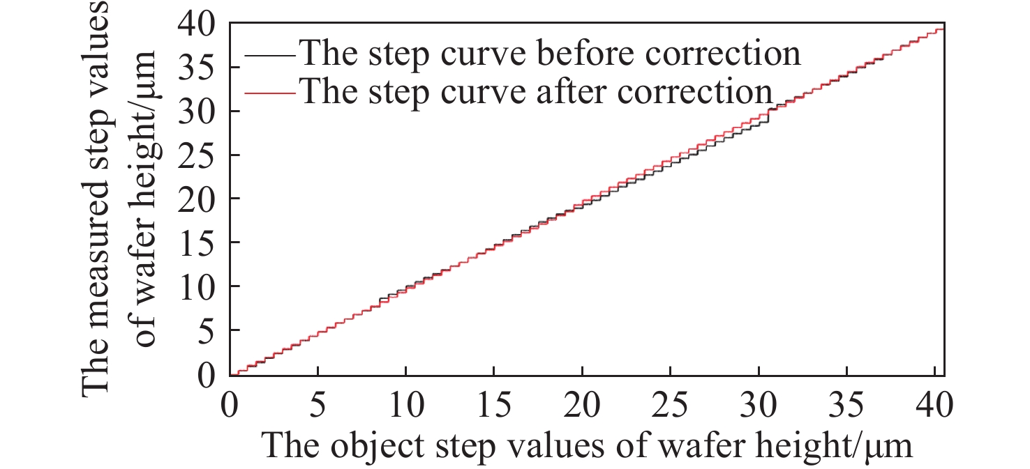
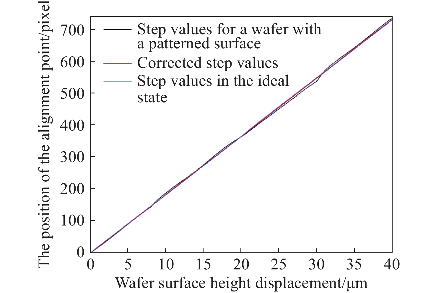
图 21 步进过程中数字光栅测量的位移值
Figure 21. Displacement values measured by the digital grating during stepping
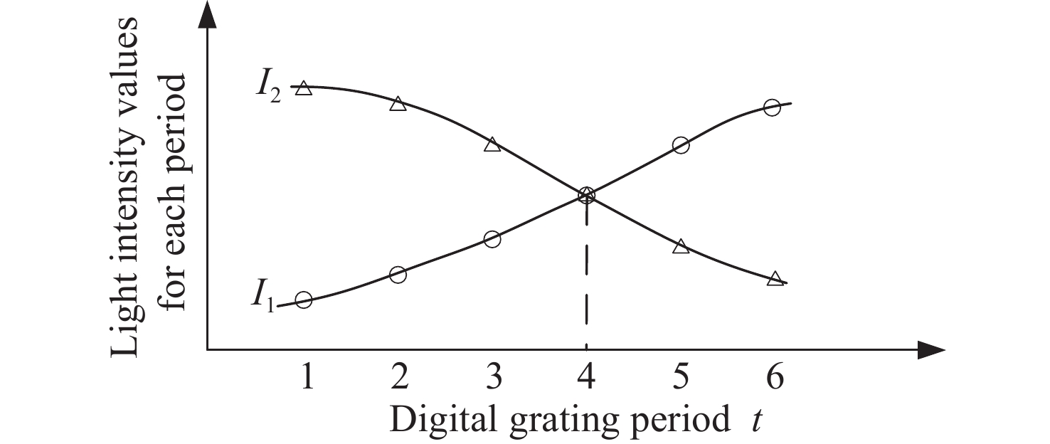
表 1 类比数字光栅和游标卡尺
Table 1. Analogical to digital gratings and vernier calipers
数字光栅 游标卡尺 主尺 相机的像素阵列 机械主尺 游标尺 周期性光栅像 机械游标尺 原理 利用周期差对微小位移进行“放大” 方法 求解光强曲线零点 找刻度对准点读数 分辨率 高于周期差 两尺的周期差  下载: 导出CSV
-
[1] 郭杰, 李世光, 赵焱, 等. 电子束硅片图形检测系统中的纳米级对焦控制技术[J]. 中国光学,2019,12(2):242-255. doi: 10.3788/co.20191202.0242GUO J, LI SH G, ZHAO Y, et al. Nano-scale focus control technology in electron beam wafer pattern inspection system[J]. Chinese Optics, 2019, 12(2): 242-255. (in Chinese). doi: 10.3788/co.20191202.0242 [2] 高旭, 李舒航, 马庆林, 等. 光栅精密位移测量技术发展综述[J]. 中国光学,2019,12(4):741-752. doi: 10.3788/co.20191204.0741GAO X, LI SH H, MA Q L, et al. Development of grating-based precise displacement measurement technology[J]. Chinese Optics, 2019, 12(4): 741-752. (in Chinese). doi: 10.3788/co.20191204.0741 [3] 李琛毅. 基于数字光栅的新型光栅尺的研究[D]. 北京: 中国科学院大学, 2021: 22-30.LI CH Y. A novel optical encoder based on digital grating[D]. Beijing: University of Chinese Academy of Sciences, 2021: 22-30. (in Chinese). [4] 钟志坚, 李琛毅, 李世光, 等. 先进光刻中的聚焦控制预算(I)-光路部分[J]. 中国光学,2021,14(5):1104-1119. doi: 10.37188/CO.2021-0033ZHONG ZH J, LI CH Y, LI SH G, et al. Budget analysis of focus control in advanced lithography (I) -optical path[J]. Chinese Optics, 2021, 14(5): 1104-1119. (in Chinese). doi: 10.37188/CO.2021-0033 [5] ASML Netherlands B. V. te Veldhoven. Level sensor and lithographic apparatus: NL, 2022732A[P]. 2019-10-16. [6] Canon Kabushiki Kaisha. Lithography apparatus, lithography method, and method of manufacturing article: US, 10488764B2[P]. 2019-11-26. [7] 孙裕文, 李世光, 宗明成. 基于空间分光的纳米级调焦调平测量技术[J]. 光学学报,2016,36(5):0512002. doi: 10.3788/AOS201636.0512002SUN Y W, LI SH G, ZONG M CH. Nanoscale focusing and leveling measurement technology based on optical spatial split[J]. Acta Optica Sinica, 2016, 36(5): 0512002. (in Chinese). doi: 10.3788/AOS201636.0512002 [8] 冯金花, 胡松, 李艳丽, 等. 基于叠栅条纹相位解析的纳米检焦方法[J]. 光学学报,2015,35(2):0212005. doi: 10.3788/AOS201535.0212005FENG J H, HU S, LI Y L, et al. Nano focusing method based on moire fringe phase analysis[J]. Acta Optica Sinica, 2015, 35(2): 0212005. (in Chinese). doi: 10.3788/AOS201535.0212005 [9] 蓝科, 陈雪影, 刘逍. 沟槽晶圆调焦调平测量工艺适应性分析[J]. 中国设备工程,2021(13):125-127.LAN K, CHEN X Y, LIU X. Adaptability analysis of measurement technology of Groove Wafer focusing and leveling[J]. China Plant Engineering, 2021(13): 125-127. (in Chinese). [10] 郭磊. 数字光刻机中的三维位移测量系统研究[D]. 北京: 中国科学院大学, 2022: 25-31.GUO L. Three-dimensional displacement measurement system in digital lithographic system[D]. Beijing: University of Chinese Academy of Sciences, 2022: 25-31. (in Chinese). [11] 苏绍璟. 大量程纳米级光栅位移测量理论及关键技术研究[D]. 长沙: 国防科学技术大学, 2001: 37-43.SU SH J. Research on theory and key technologies of long-range displacement measuring with nanometer resolution by grating[D]. Changsha: National University of Defense Technology, 2001: 37-43. (in Chinese). [12] 邢丽冬, 潘双来. 信号与线性系统[M]. 3版. 北京: 清华大学出版社, 2020: 59-127.XING L D, PAN SH L. Signal & Linear Systems[M]. 3rd ed. Beijing: Tsinghua University Press, 2020: 59-127. (in Chinese). [13] LEVINSON H J. Principles of Lithography[M]. 3rd ed. Bellingham, USA: SPIE, 2010: 32-46. [14] 李小平, 陈飞彪. 投影光刻机硅片调焦调平测量模型[J]. 光学学报,2007,27(11):1987-1991. doi: 10.3321/j.issn:0253-2239.2007.11.013LI X P, CHEN F B. Measurement model of focusing and leveling measurement system for projection lithography tool[J]. Acta Optica Sinica,2007,27(11):1987-1991. (in Chinese) doi: 10.3321/j.issn:0253-2239.2007.11.013 -

 下载:
下载:


计量
- 文章访问数: 601
- HTML全文浏览量: 399
- PDF下载量: 192
- 被引次数: 0
