


-
摘要:
本文利用基于光束传播方法的有限元仿真模型研究了氮化镓(GaN)平面光波导的传输损耗特性,并针对传统GaN波导损耗较大的问题提出了工艺优化方案。通过构建完整的传输损耗模型,系统分析了波导几何参数对传输特性的影响,重点研究了顶部刻蚀和背后减薄两种优化工艺的改善效果。研究结果表明,这两种工艺均可显著降低波导传输损耗。其中顶部刻蚀工艺和背后减薄工艺可将损耗从2.29 dB/mm分别降至0.19 dB/mm和0.24 dB/mm。此外,本文还量化分析了制造工艺引入的侧壁夹角和表面粗糙度等缺陷对传输损耗的影响,并通过参数优化确定了实现可见光单模传输的关键结构尺寸。本文研究成果为设计和制备低损耗GaN平面光波导提供了理论依据和工艺指导。
Abstract:In this paper, we investigate the transmission loss characteristics of gallium nitride (GaN) planar optical waveguides using a finite element simulation model based on the beam propagation method (BPM). To address the high transmission loss in conventional GaN waveguides, we propose process optimization solutions. By constructing a comprehensive transmission loss model, we systematically analyze the impact of waveguide geometric parameters on the transmission characteristics, with a particular focus on investigating the improvement effects of two optimization processes: top etching and back thinning. The experiment results indicate that both processes significantly reduce the waveguide transmission loss, with the top etching process reducing loss from 2.29 dB/mm to 0.19 dB/mm and the back thinning process reducing it to 0.24 dB/mm. Additionally, we analyze the impact of manufacturing defects, such as sidewall angles and surface roughness, on transmission loss. Through parameter optimization, we identify the key dimensions necessary for single mode light transmission. This study provides a theoretical basis and process guidance for the development of low-loss GaN waveguides.
-
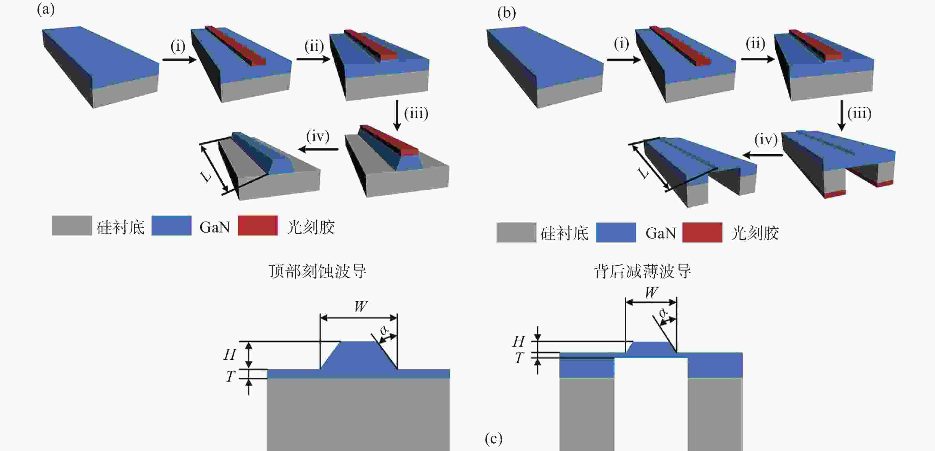
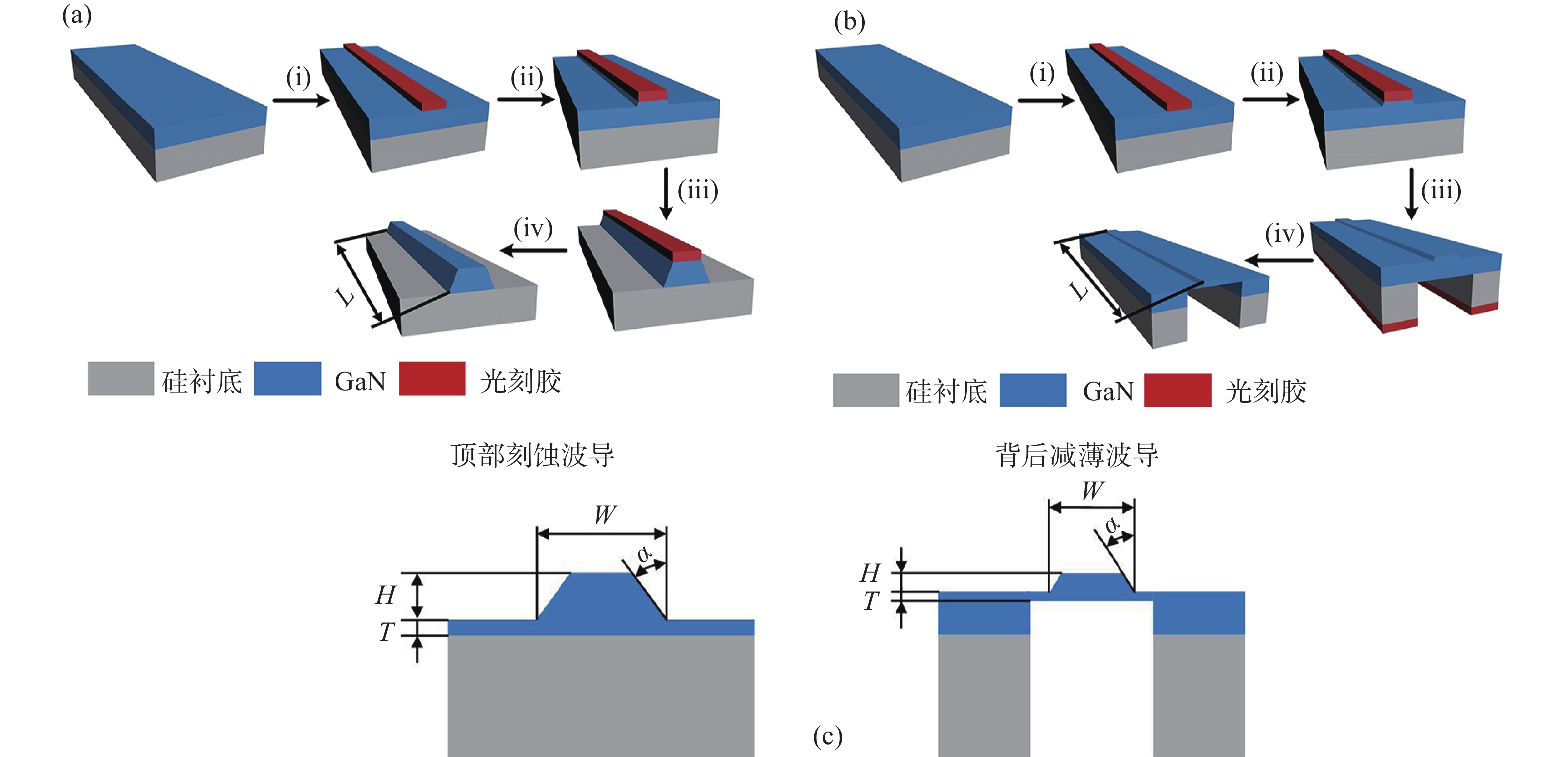
图 1 (a) 顶部刻蚀GaN平面光波导和(b) 背后减薄GaN平面光波导的加工流程图;(c) 两种GaN平面光波导的横截面示 意图
Figure 1. Processing flow charts of the GaN planar optical waveguide obtained by (a) top etching and (b) bock thinning processes. (c) The cross-sectional diagrams of the two types of GaN planar optical waveguide
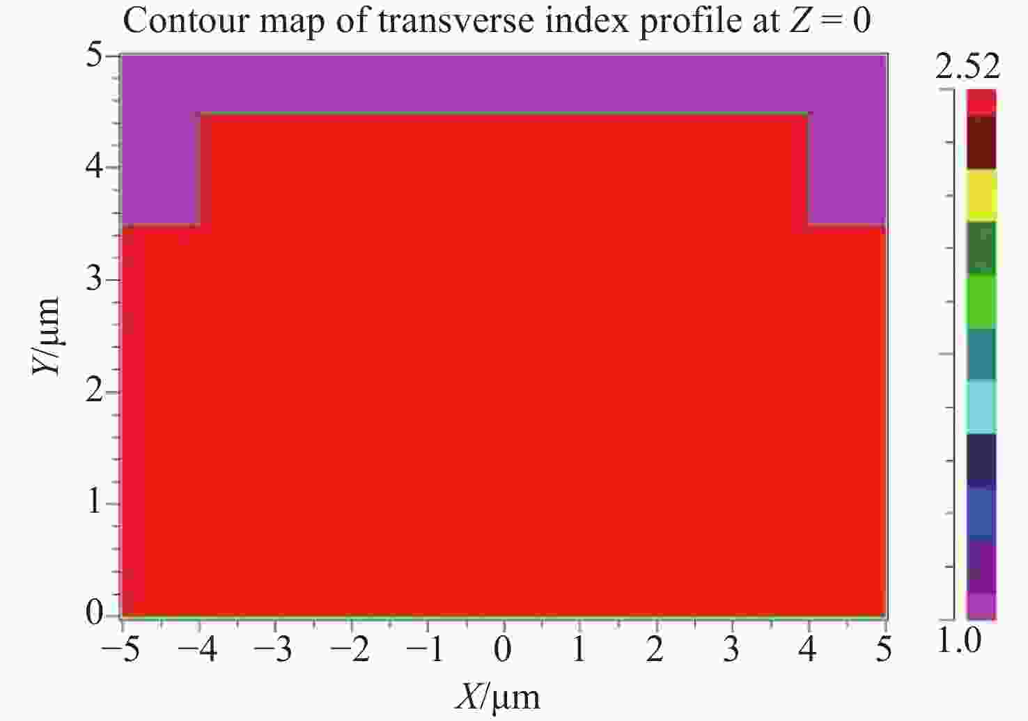
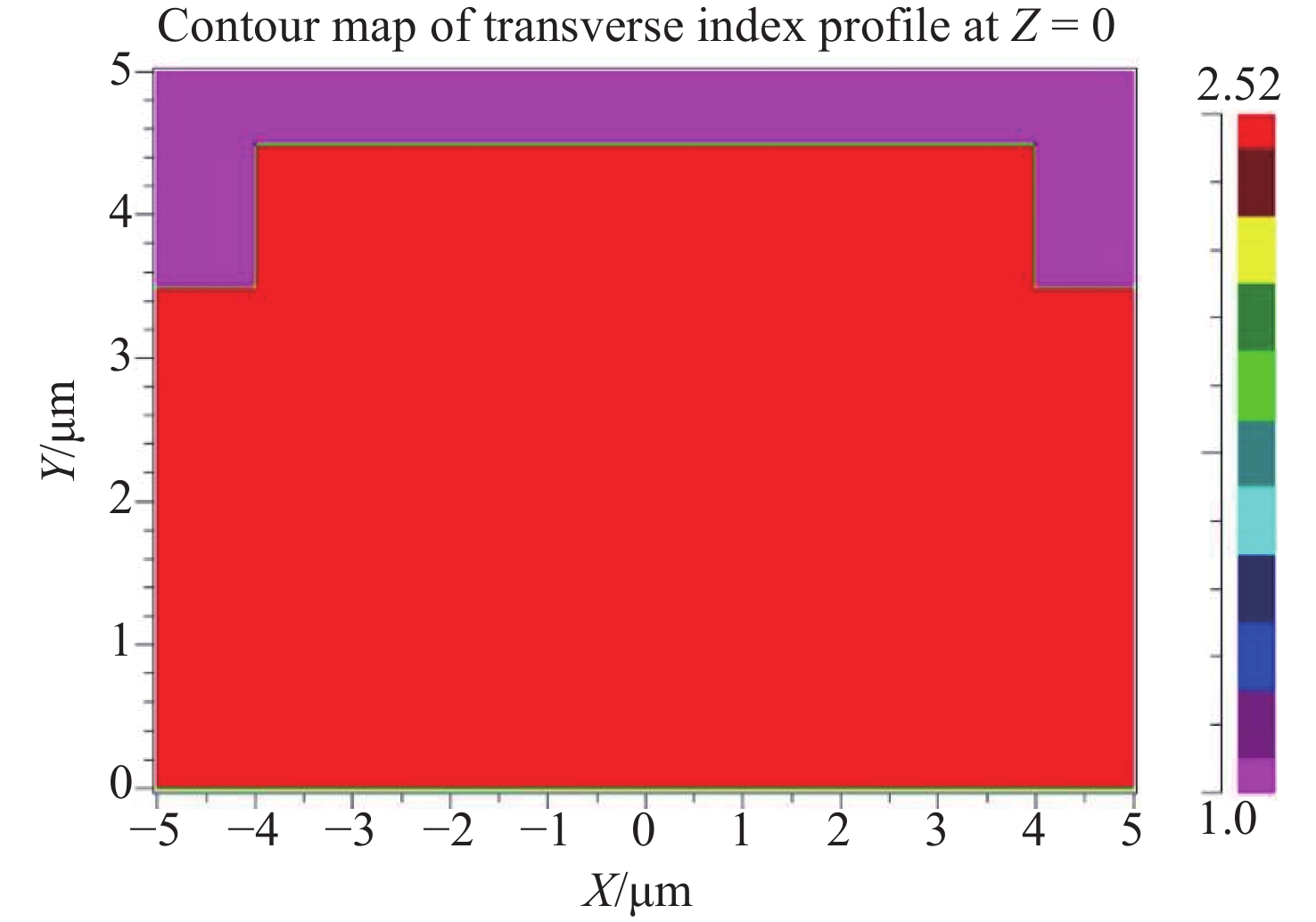
图 2 初始模型下GaN平面光波导的折射率分布图
Figure 2. Refractive index distribution of GaN planar optical waveguides under the initial model
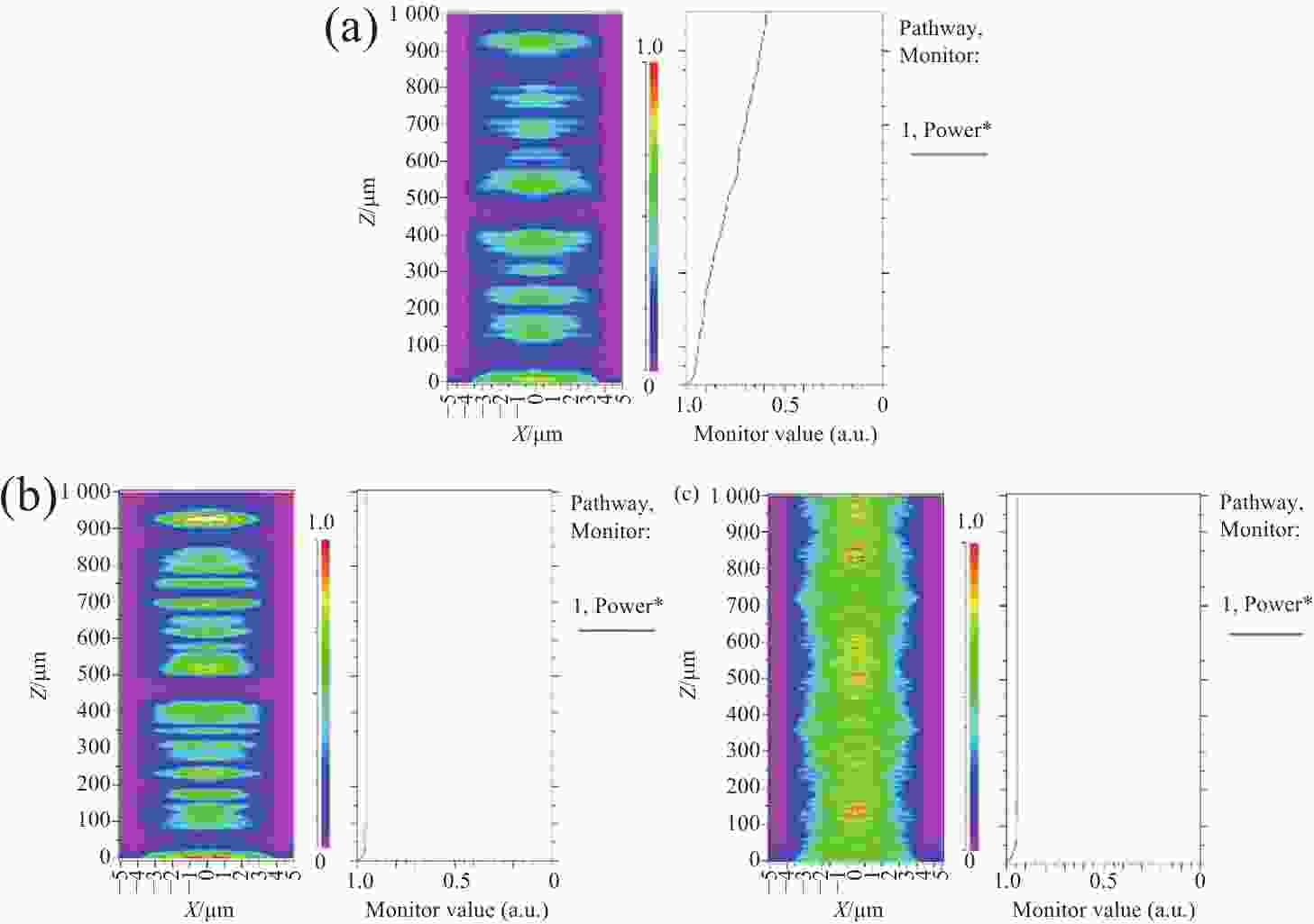
图 3 GaN平面光波导的相对光功率分布(波导传输方向)。(a) 初始模型;(b) 顶部刻蚀工艺去除脊型波导下方平板层;(c) 背后减薄工艺去除脊型波导下方平板层
Figure 3. Relative light output distribution of GaN planar optical waveguide (in waveguide transmission direction). (a) Initial model; (b) top etching process and (c) back thinning process removing the lower flat layer of ridge waveguide
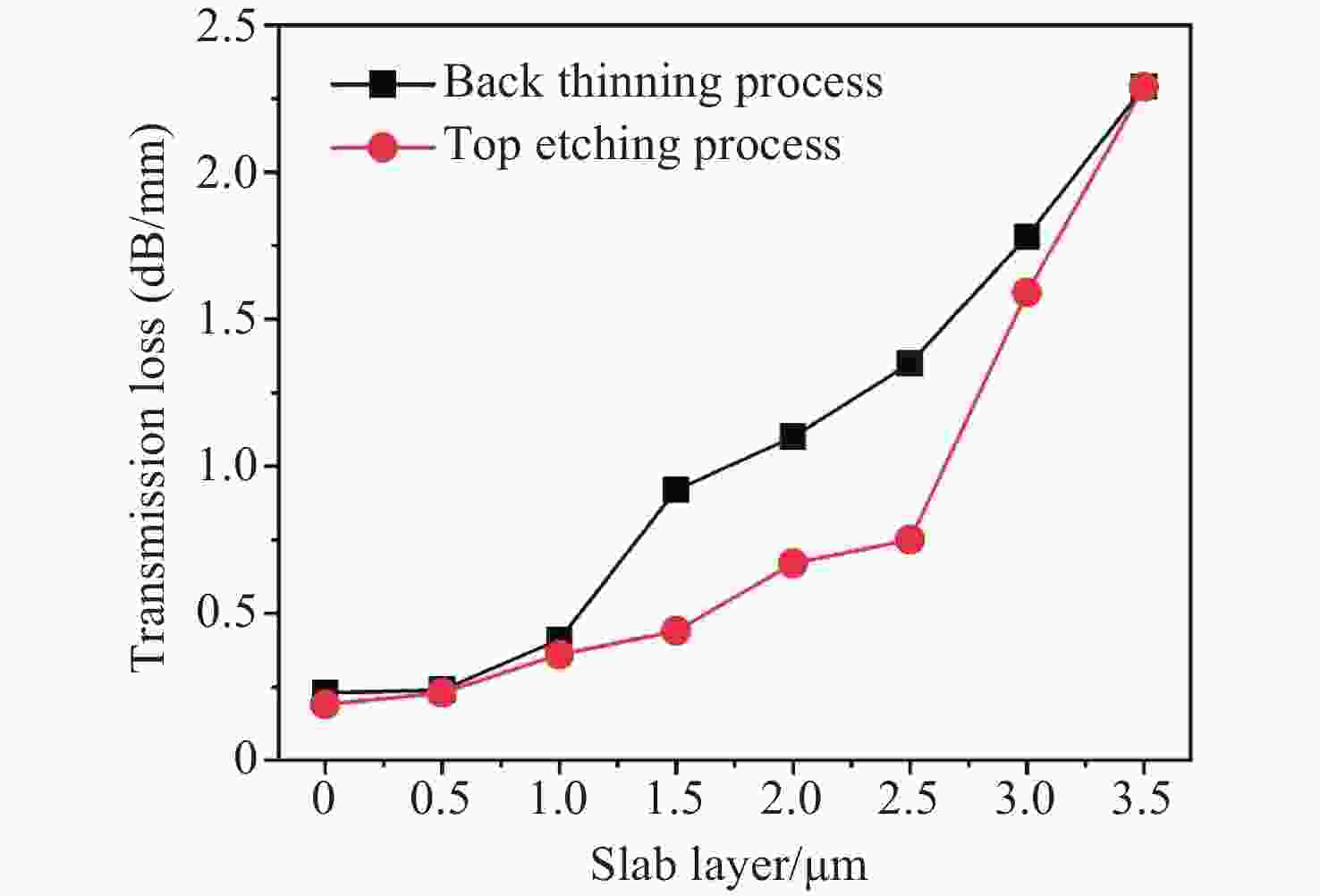
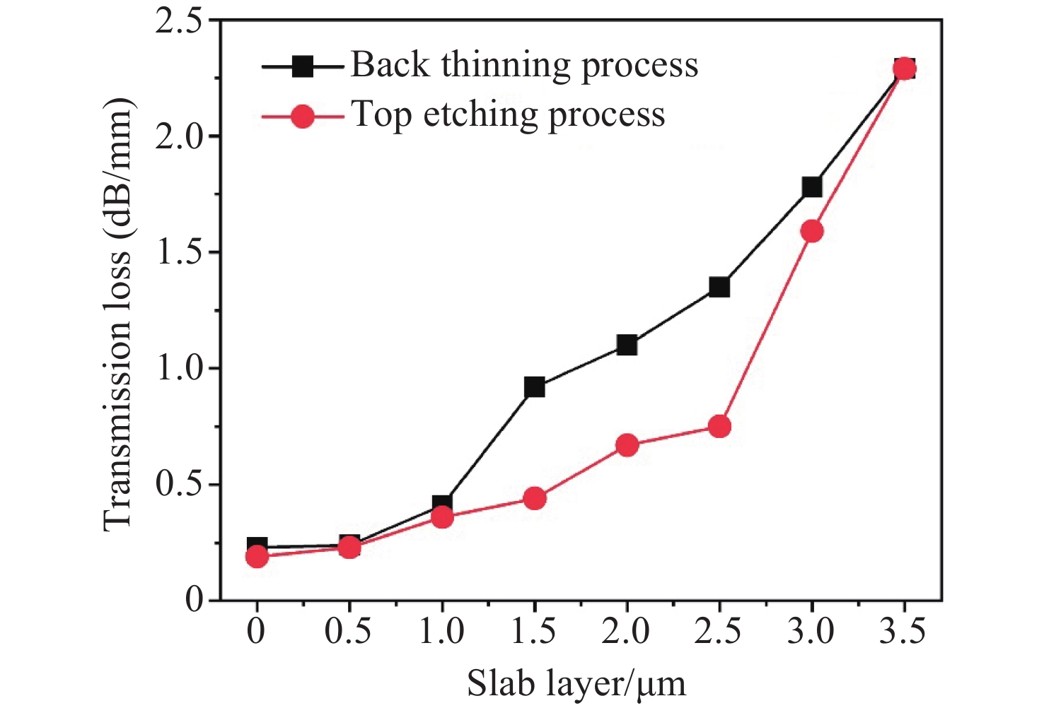
图 4 两种不同工艺下氮化镓波导传输损耗随平板层厚度变化曲线
Figure 4. GaN waveguide’s transmission loss varying with plate thickness for two different processes
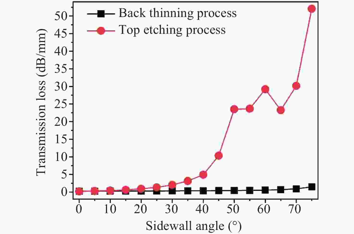
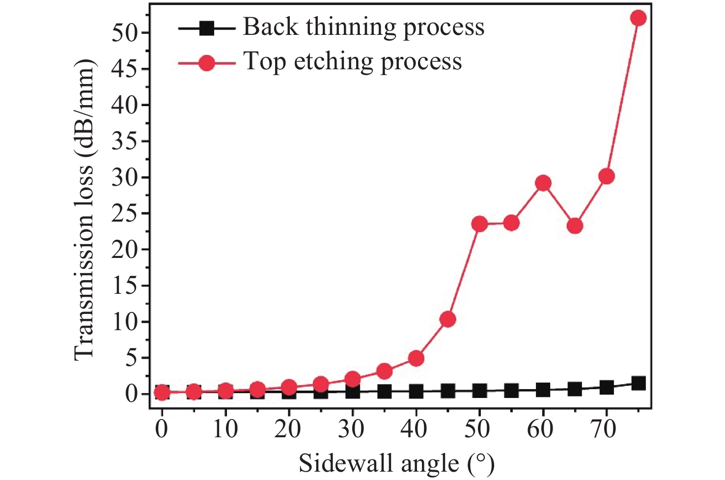
图 5 两种不同工艺下,氮化镓波导的传输损耗随侧壁夹角变化曲线
Figure 5. GaN waveguide’s transmission loss varying with sidewall angle for two different processes
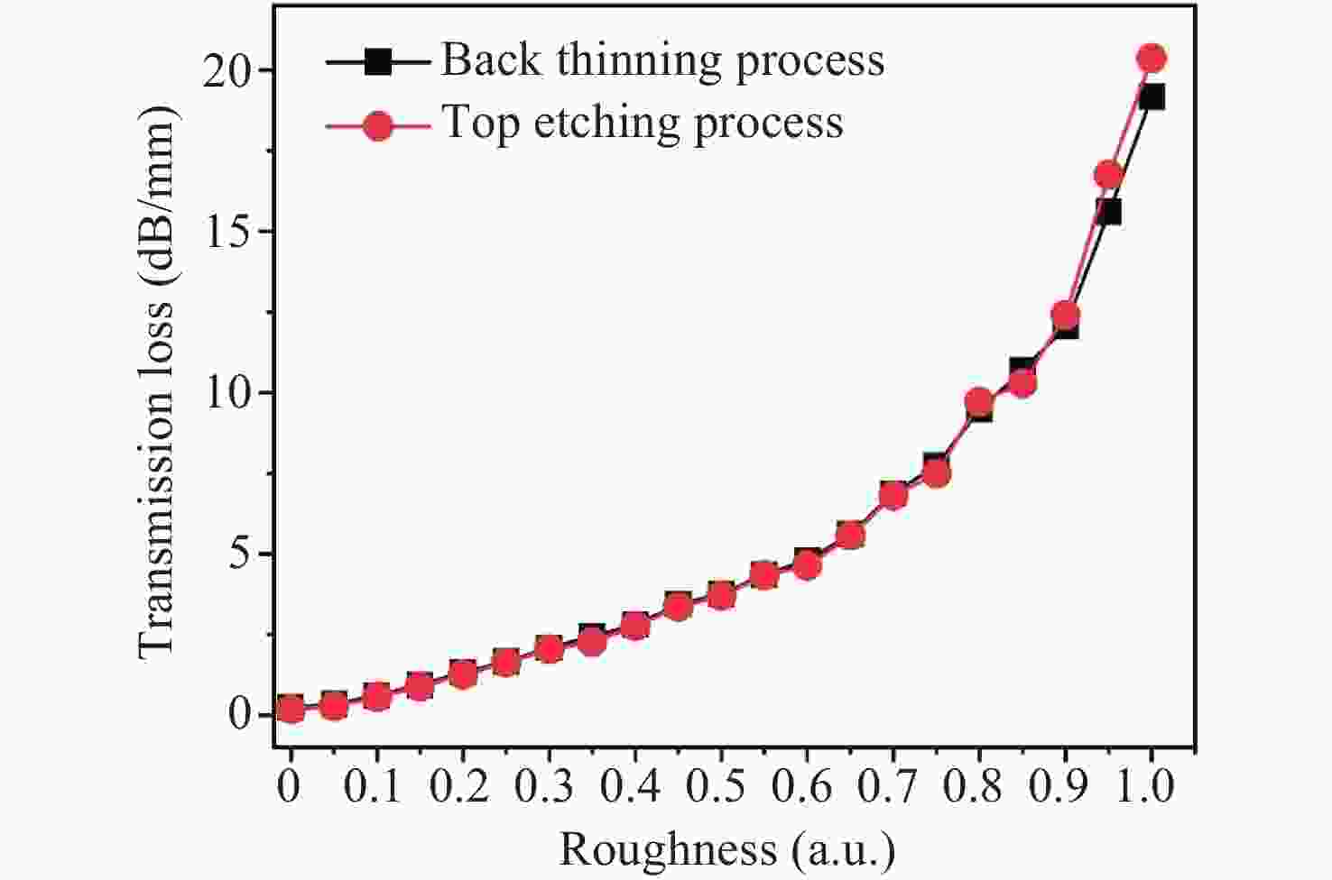
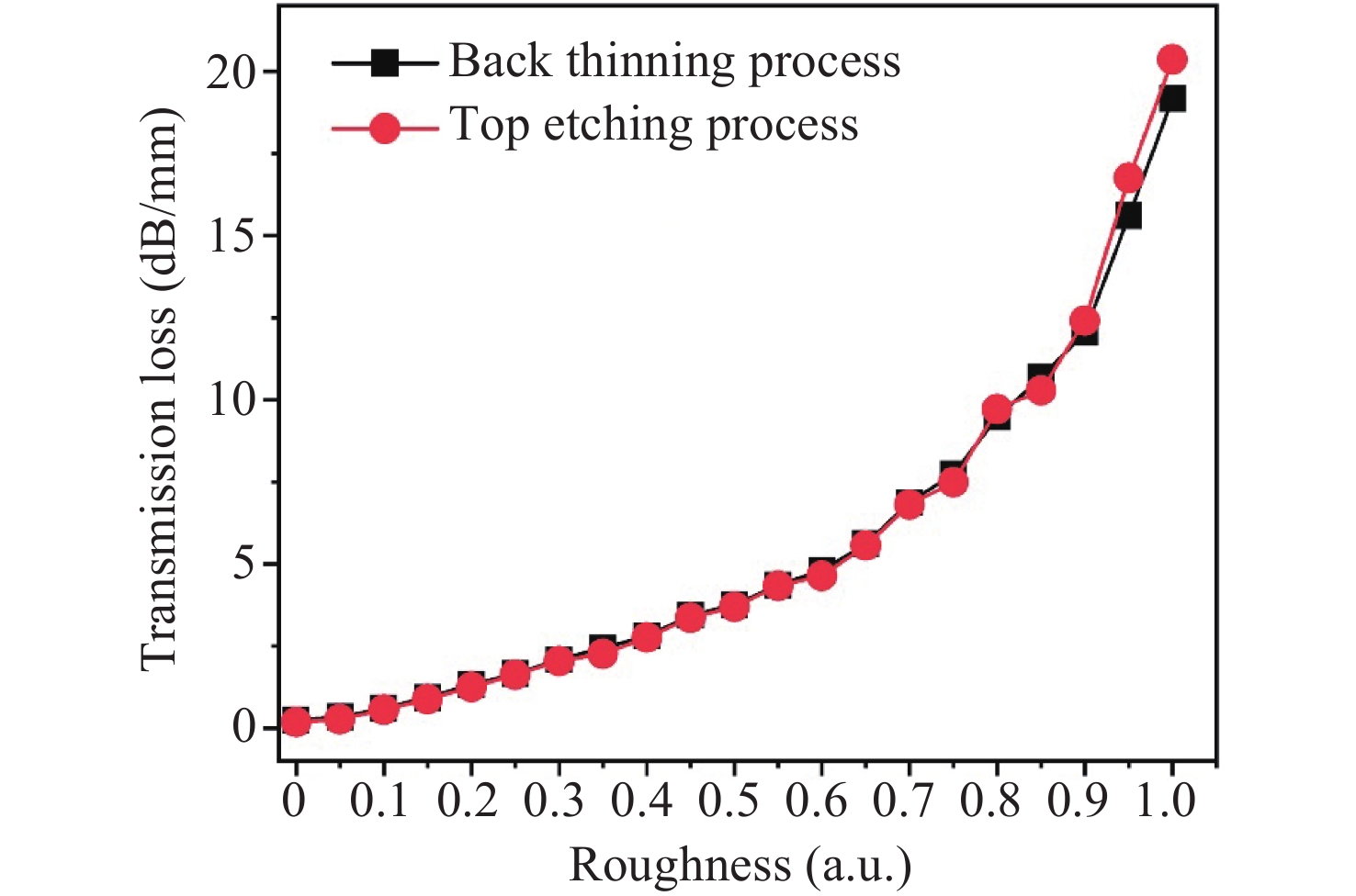
图 6 两种不同工艺下,氮化镓波导传输损耗随粗糙度变化曲线
Figure 6. GaN waveguide’s transmission loss varying with roughness for two different processes
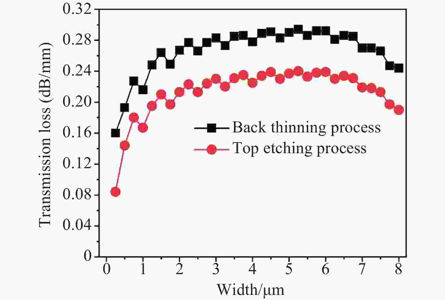
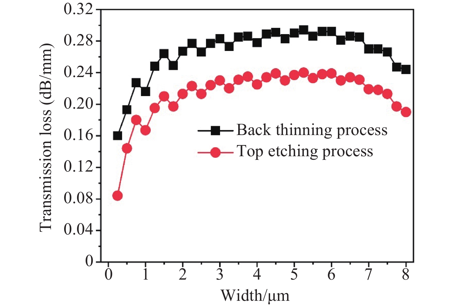
图 7 两种不同工艺下,氮化镓波导传输损耗随波导宽度变化曲线
Figure 7. GaN waveguide’s transmission loss varying with waveguide width for two different processes
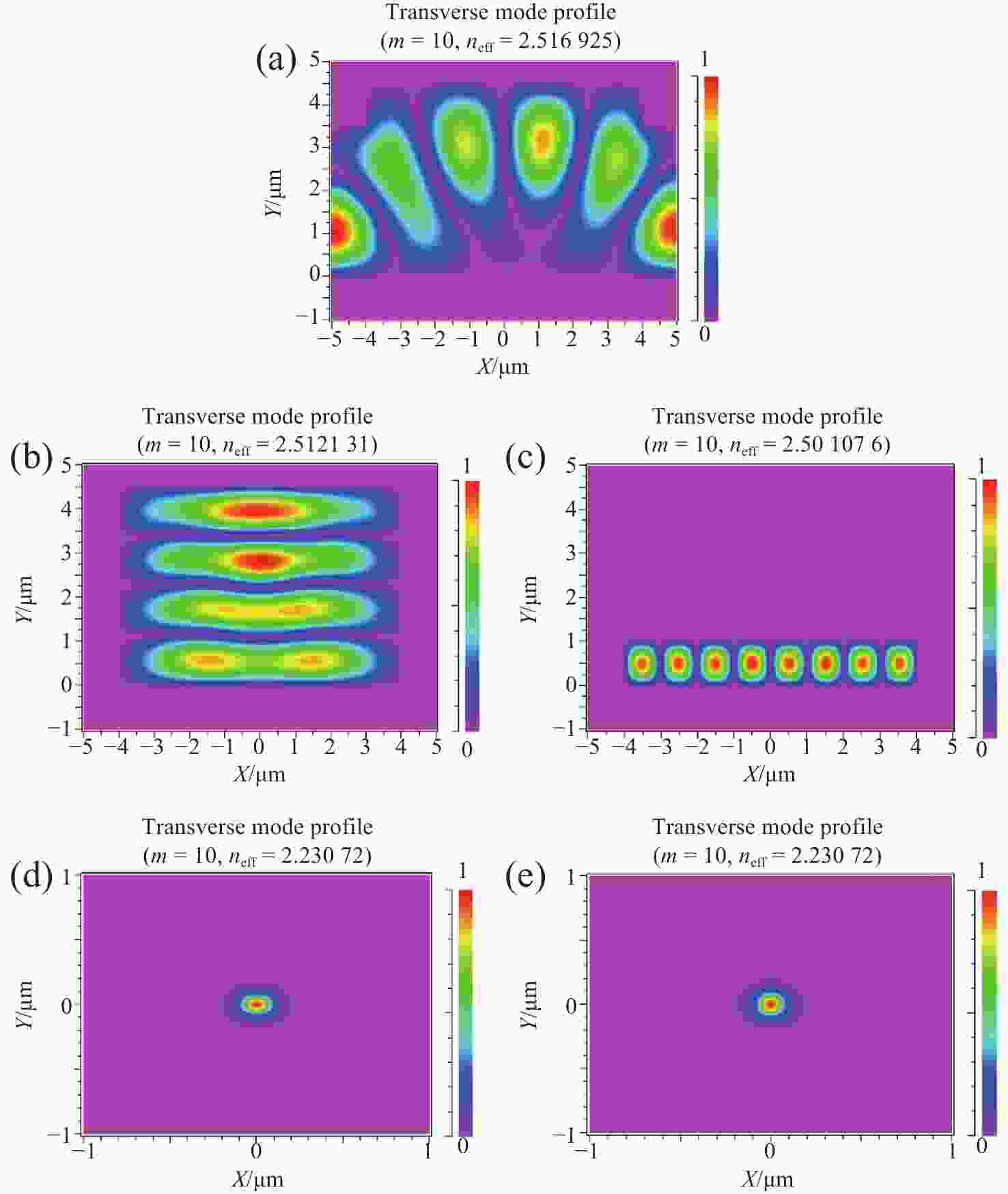
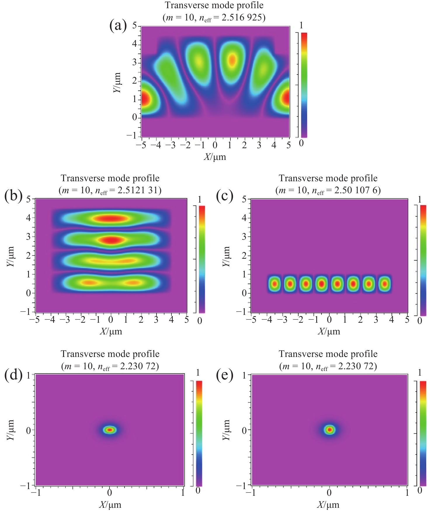
图 8 氮化镓波导的光场传输模式分析(波导横截面)。(a) 初始模型;(b) 顶部刻蚀工艺去除平板层;(c) 背后减薄工艺去除平板层;(d) 波导宽度为150 nm、高度为100 nm实现单模传输;(e) 波导宽度为100 nm、高度为150 nm实现单模传输
Figure 8. Analysis of light field transmission mode of GaN waveguide (waveguide cross section). (a) Initial model; (b) top etching process and (c) back thinning process removing the flat layer; single-mode transmission achieved by waveguide (d) with width of 150 nm and height of 100 nm, and (e) with width of 100 nm and height of 150 nm
-
[1] ISMAIL S N, SALIH M H. A review of visible light communication (VLC) technology[J]. AIP Conference Proceedings, 2020, 2213(1): 020289. [2] 徐宪莹, 岳殿武. 可见光通信中正交频分复用调制技术[J]. 中国光学,2021,14(3):516-527. doi: 10.37188/CO.2020-0051XU X Y, YUE D W. Orthogonal frequency division multiplexing modulation techniques in visible light communication[J]. Chinese Optics, 2021, 14(3): 516-527. (in Chinese). doi: 10.37188/CO.2020-0051 [3] 迟楠, 贾俊连. 面向6G的可见光通信[J]. 中兴通讯技术,2020,26(2):11-19. doi: 10.12142/ZTETJ.202002003CHI N, JIA J L. Visible light communication towards 6G[J]. ZTE Technology Journal, 2020, 26(2): 11-19. (in Chinese). doi: 10.12142/ZTETJ.202002003 [4] 邝海, 黄振, 熊志华, 等. 氮化镓基Micro-LED侧壁对外量子效率的影响及侧壁处理技术综述[J]. 中国光学(中英文),2023,16(6):1305-1317. doi: 10.37188/CO.2023-0091KUANG H, HUANG ZH, XIONG ZH H, et al. A review of the effect of GaN-based micro-LED sidewall on external quantum efficiency and sidewall treatment techniques[J]. Chinese Optics, 2023, 16(6): 1305-1317. (in Chinese). doi: 10.37188/CO.2023-0091 [5] JAMES SINGH K, HUANG Y M, AHMED T, et al. Micro-LED as a promising candidate for high-speed visible light communication[J]. Applied Sciences, 2020, 10(20): 7384. doi: 10.3390/app10207384 [6] XIE E Y, BIAN R, HE X Y, et al. Over 10 Gbps VLC for long-distance applications using a GaN-based series-biased micro-LED array[J]. IEEE Photonics Technology Letters, 2020, 32(9): 499-502. doi: 10.1109/LPT.2020.2981827 [7] ZHANG H, YAN J B, YE Z Q, et al. Monolithic GaN optoelectronic system on a Si substrate[J]. Applied Physics Letters, 2022, 121(18): 181103. doi: 10.1063/5.0125324 [8] GAO X M, LIU P ZH, YIN Q X, et al. Wireless light energy harvesting and communication in a waterproof GaN optoelectronic system[J]. Communications Engineering, 2022, 1(1): 16. doi: 10.1038/s44172-022-00016-5 [9] XU F F, QIU P J, TAO T, et al. High bandwidth semi-polar InGaN/GaN micro-LEDs with low current injection for visible light communication[J]. IEEE Photonics Journal, 2023, 15(1): 7300704. [10] SMITH J A, SMITH J A, HILL P, et al. High precision integrated photonic thermometry enabled by a transfer printed diamond resonator on GaN waveguide chip[J]. Optics Express, 2021, 29(18): 29095-29106. doi: 10.1364/OE.433607 [11] RATHKANTHIWAR S S, RAGHAVAN S, SELVARAJA S K. Polarization independent grating in a GaN-on-sapphire photonic integrated circuit[J]. Optics Express, 2023, 31(14): 23350-23361. doi: 10.1364/OE.487389 [12] YAN J, FANG L, SUN Z, et al. Complete active-passive photonic integration based on GaN-on-silicon platform[J]. Advanced Photonics Nexus, 2023, 2(4): 046003. [13] 陶京. 浅刻蚀弧形SOI脊形波导侧向泄漏分析与器件设计[D]. 杭州: 浙江工业大学, 2017.TAO J. Lateral leakage loss analysis and device design of shallow-etched rib waveguide on soi with arc cross-section[D]. Hangzhou: Zhejiang University of Technology, 2017. (in Chinese). [14] 刘军. SOI脊形光波导损耗研究[D]. 长沙: 国防科学技术大学, 2010.LIU J. Loss research on rib waveguide[D]. Changsha: National University of Defense Technology, 2010. (in Chinese). [15] 梁宇雷. 平面光波导损耗测试[D]. 长春: 吉林大学, 2004.LIANG Y L. Measurement of slab optical waveguide losses[D]. Changchun: Jilin University, 2004. (in Chinese). [16] SOREF R. The past, present, and future of silicon photonics[J]. IEEE Journal of Selected Topics in Quantum Electronics, 2006, 12(6): 1678-1687. doi: 10.1109/JSTQE.2006.883151 [17] SHAKYA J, LIN J Y, JIANG H X. Near-field optical study of AlGaN/GaN quantum-well waveguide[J]. Applied Physics Letters, 2004, 84(11): 1832-1834. doi: 10.1063/1.1675936 [18] GROMOVYI M, SEMOND F, DUBOZ J Y, et al. Low loss GaN waveguides for visible light on Si substrates[J]. Journal of the European Optical Society-Rapid Publications, 2014, 9: 14050. doi: 10.2971/jeos.2014.14050 [19] CHEN H, FU H Q, HUANG X Q, et al. Low loss GaN waveguides at the visible spectral wavelengths for integrated photonics applications[J]. Optics Express, 2017, 25(25): 31758-31773. doi: 10.1364/OE.25.031758 [20] ISHIHARA H, SHIMADA K, UMEDA S, et al. Fabrication and evaluation of rib-waveguide-type wavelength conversion devices using GaN-QPM crystals[J]. Japanese Journal of Applied Physics, 2022, 61(SK): SK1020. doi: 10.35848/1347-4065/ac727a [21] SEKIYA T, SASAKI T, HANE K. Design, fabrication, and optical characteristics of freestanding GaN waveguides on silicon substrate[J]. Journal of Vacuum Science & Technology B, 2015, 33(3): 031207. [22] CAI Y F, WU K Y, MA ZH P, et al. Integration of large-extinction-ratio resonators with grating couplers and waveguides on GaN-on-sapphire at O-band[J]. Optics Express, 2023, 31(26): 42795-42806. [23] O’BRIEN M, MARAVIGLIA N, UZUN A, et al. Integration of O-band quantum dot lasers with AlGaN/GaN waveguides[J]. Optics Express, 2024, 32(13): 23047-23055. doi: 10.1364/OE.527790 [24] WATANABE N, KIMOTO T, SUDA J. The temperature dependence of the refractive indices of GaN and AlN from room temperature up to 515°C[J]. Journal of Applied Physics, 2008, 104(10): 106101. doi: 10.1063/1.3021148 [25] WU X Y, FENG J J, LIU X T, et al. Effects of rapid thermal annealing on aluminum nitride waveguides[J]. Optical Materials Express, 2020, 10(12): 3073-3080. doi: 10.1364/OME.410129 [26] LI X, WANG Y J, HANE K, et al. GaN-based integrated photonics chip with suspended LED and waveguide[J]. Optics Communications, 2018, 415: 43-47. doi: 10.1016/j.optcom.2017.12.077 [27] LI X, JIANG Y, LI J, et al. Integrated photonics chip with InGaN/GaN light-emitting diode and bended waveguide for visible-light communications[J]. Optics & Laser Technology, 2019, 114: 103-109. [28] LI X, JIANG Y, NI S Y, et al. Freestanding GaN-based integrated photonics chip with ultra-micro LED and straight waveguide for visible light communication[J]. Proceedings of SPIE, 2018, 10814: 108140N. [29] 李欣, 王徐, 李芸, 等. 面向可见光通信的硅基InGaN/GaN多量子阱多口分路器光子集成芯片[J]. 电子与信息学报,2022,44(8):2649-2658. doi: 10.11999/JEIT210953LI X, WANG X, LI Y, et al. Silicon-based InGaN/GaN multi-quantum wells multi-port splitter photonic integrated chip for visible light communication[J]. Journal of Electronics & Information Technology, 2022, 44(8): 2649-2658. (in Chinese). doi: 10.11999/JEIT210953 [30] 高峰, 秦丽, 陈永毅, 等. 弯曲波导研究进展及其应用[J]. 中国光学,2017,10(2):176-193. doi: 10.3788/co.20171002.0176GAO F, QIN L, CHEN Y Y, et al. Research progress of bent waveguide and its applications[J]. Chinese Optics, 2017, 10(2): 176-193. (in Chinese). doi: 10.3788/co.20171002.0176 [31] YU X R, WANG M K, LI J H, et al. Study on the single-mode condition for x-cut LNOI rib waveguides based on leakage losses[J]. Optics Express, 2022, 30(5): 6556-6565. doi: 10.1364/OE.451842 [32] MA ZH P, WAN Y J, ZHANG Y, et al. Broadband lateral leakage suppression for TM polarization empowered by slab-photonic-crystal-modified ridge waveguide[J]. Optics Express, 2024, 32(18): 31730-31740. doi: 10.1364/OE.531406 [33] SHI J Y, XU Z Y, NIU W Q, et al. Si-substrate vertical-structure InGaN/GaN micro-LED-based photodetector for beyond 10 Gbps visible light communication[J]. Photonics Research, 2022, 10(10): 2394-2404. doi: 10.1364/PRJ.465455 [34] HE J L, FENG M X, ZHONG Y Z, et al. On-wafer fabrication of cavity mirrors for InGaN-based laser diode grown on Si[J]. Scientific Reports, 2018, 8(1): 7922. doi: 10.1038/s41598-018-26305-8 -

 下载:
下载:


计量
- 文章访问数: 300
- HTML全文浏览量: 123
- PDF下载量: 45
- 被引次数: 0
