


Achromatic monolayer metalens with elongated field of view in a continuous waveband
-
摘要:
超构表面透镜存在离轴像差和材料色散,在成像探测领域无法同时兼顾视场和工作带宽。本文基于单片超构表面构建可见光大视场消色差超透镜。采用二次型相位实现大视场探测,进一步通过粒子群算法(particle swarm optimization, PSO)优化超构表面单元结构传输相位实现连续波段色散调控,因此在满足大视场下拓展工作带宽。对于单片超构表面透镜数值孔径0.351,在0.55 μm~0.65 μm波段内实现了±20°视场角的消色差光场聚焦。在工作波段和视场范围内焦距纵向误差≤3.2 μm(~0.08
f 0),入射角探测偏差≤1.34°。本文提出的可见连续波段大视场消色差单片超构表面透镜有望在轻小型、集成化光学系统成像探测等领域发挥作用。Abstract:Metalenses are subject to off-axis aberrations and material dispersion, which fundamentally limit their ability to achieve both wide field-of-view (FOV) and broad operational bandwidth in imaging detection systems. In this paper, an achromatic monolayer metalens with an elongated FOV in a continuous waveband is constructed using an elaborately designed metasurface. Leveraging a quadratic phase profile for large-field-of-view (FOV) detection, the metasurface unit structure transmission phase is subsequently optimized via particle swarm optimization (PSO) to achieve continuous band dispersion tuning. This approach consequently enables expanded operational bandwidth under wide-FOV conditions. For a monolayer metalens with a numerical aperture of 0.351, an achromatic focusing field covering a ±20° FOV is obtained within the continuous waveband from 0.55 μm to 0.65 μm. The maximum focal length deviation along the optical axis is 3.2 μm (~0.08
f 0), the incident angle detection deviation ≤ 1.34°. The proposed method can realize an achromatic monolayer metalens with an elongated FOV within a continuous waveband, which will have potential applications in lightweight and integrated optical imaging systems.-
Key words:
- Metalens /
- Achromatic /
- Large field of view
-
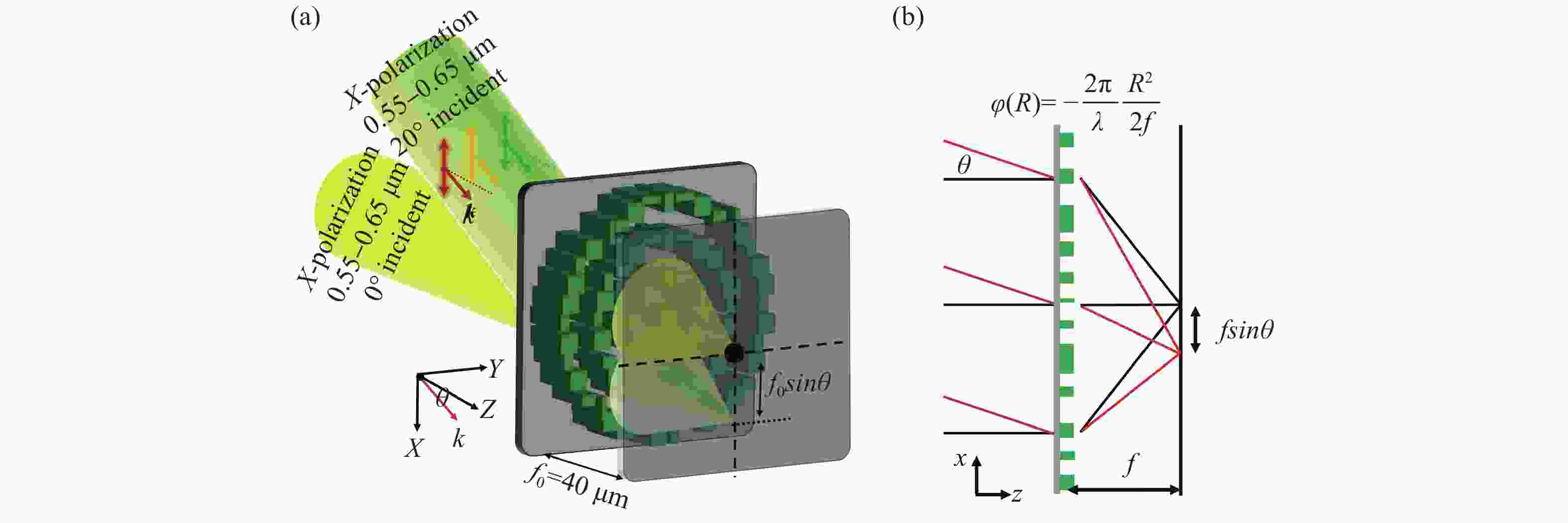
图 1 (a)大视场消色差超透镜示意图。(b)二次相位原理示意图。
Figure 1. Schematic diagram of (a) the large FOV achromatic metalens and (b) the quadratic phase principle.
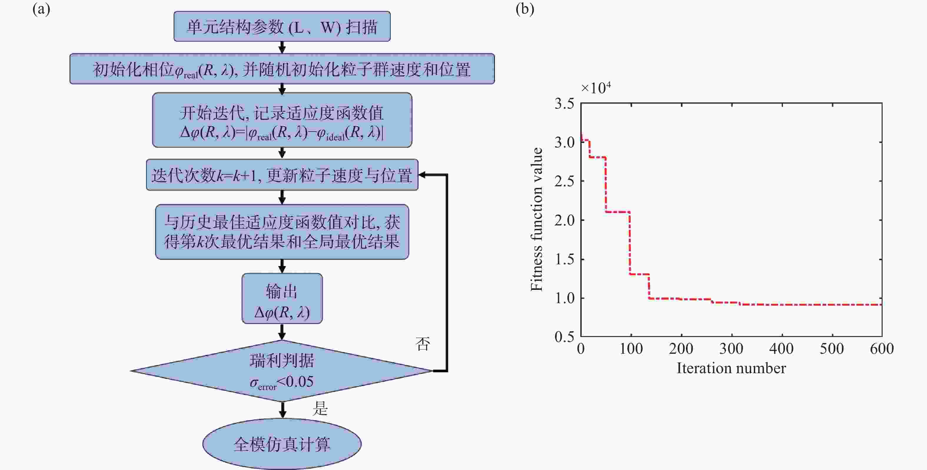
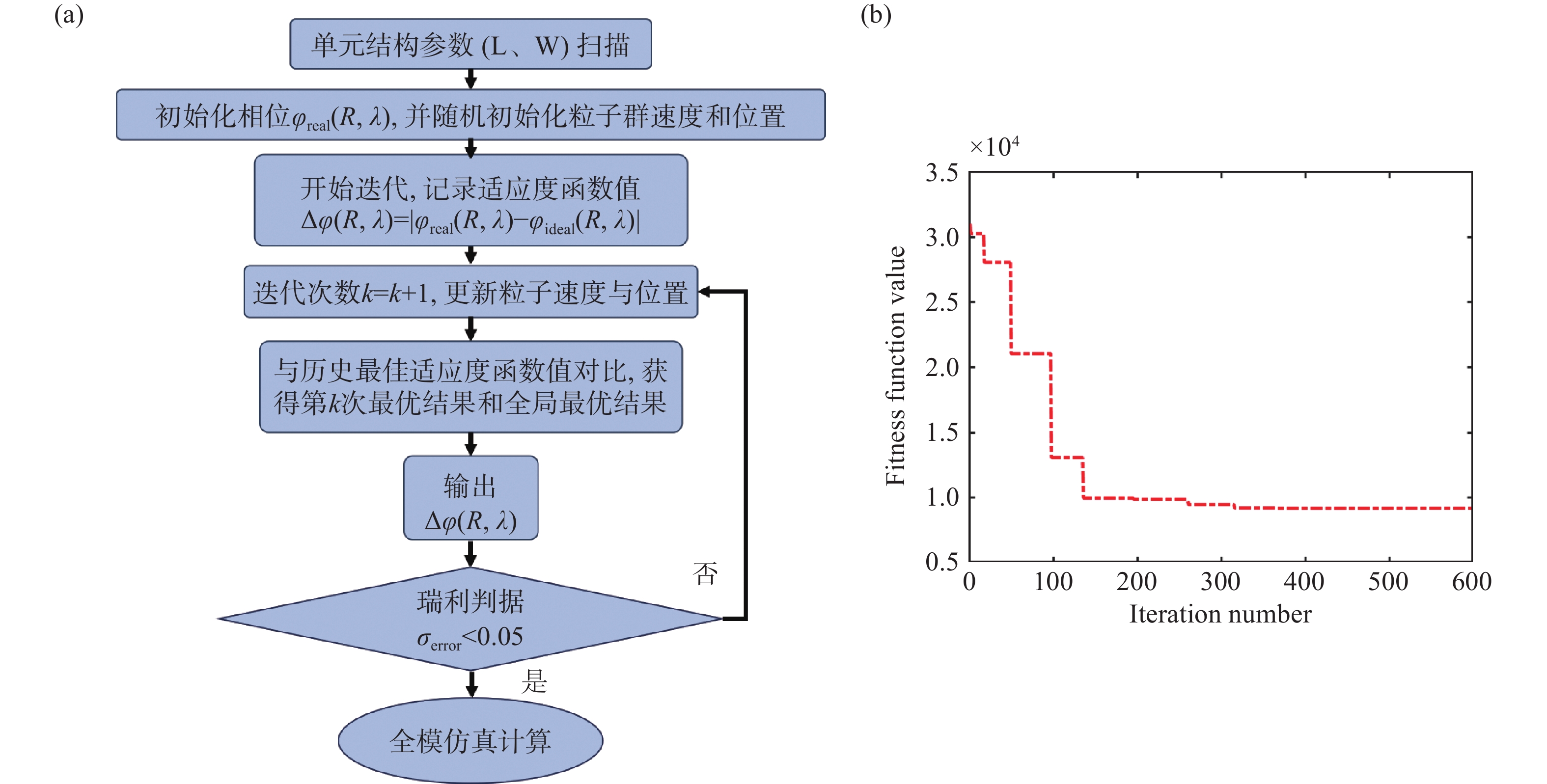
图 2 (a)粒子群算法流程图。(b) PSO收敛曲线。
Figure 2. (a) Flow chart for the particle swarm algorithm. (b) The convergence curve of PSO.
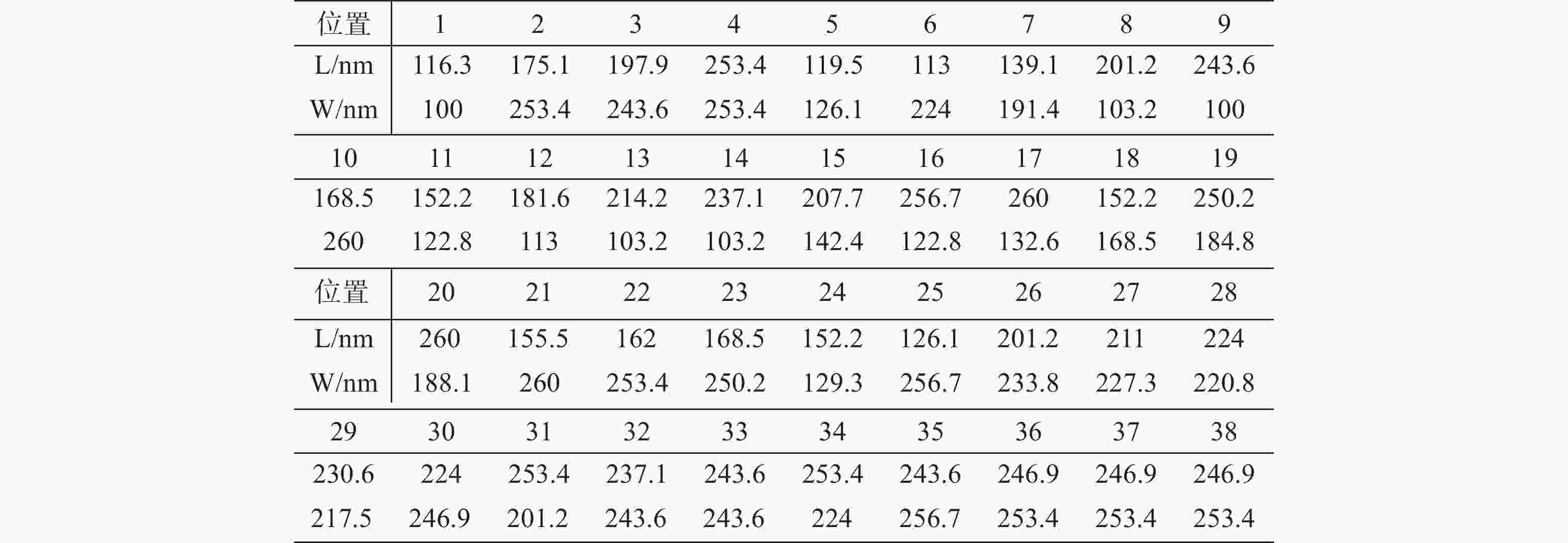
图 3 超透镜径向单元结构对应的结构参数。
Figure 3. Those structure parameters of the radial unit cells for metalens.

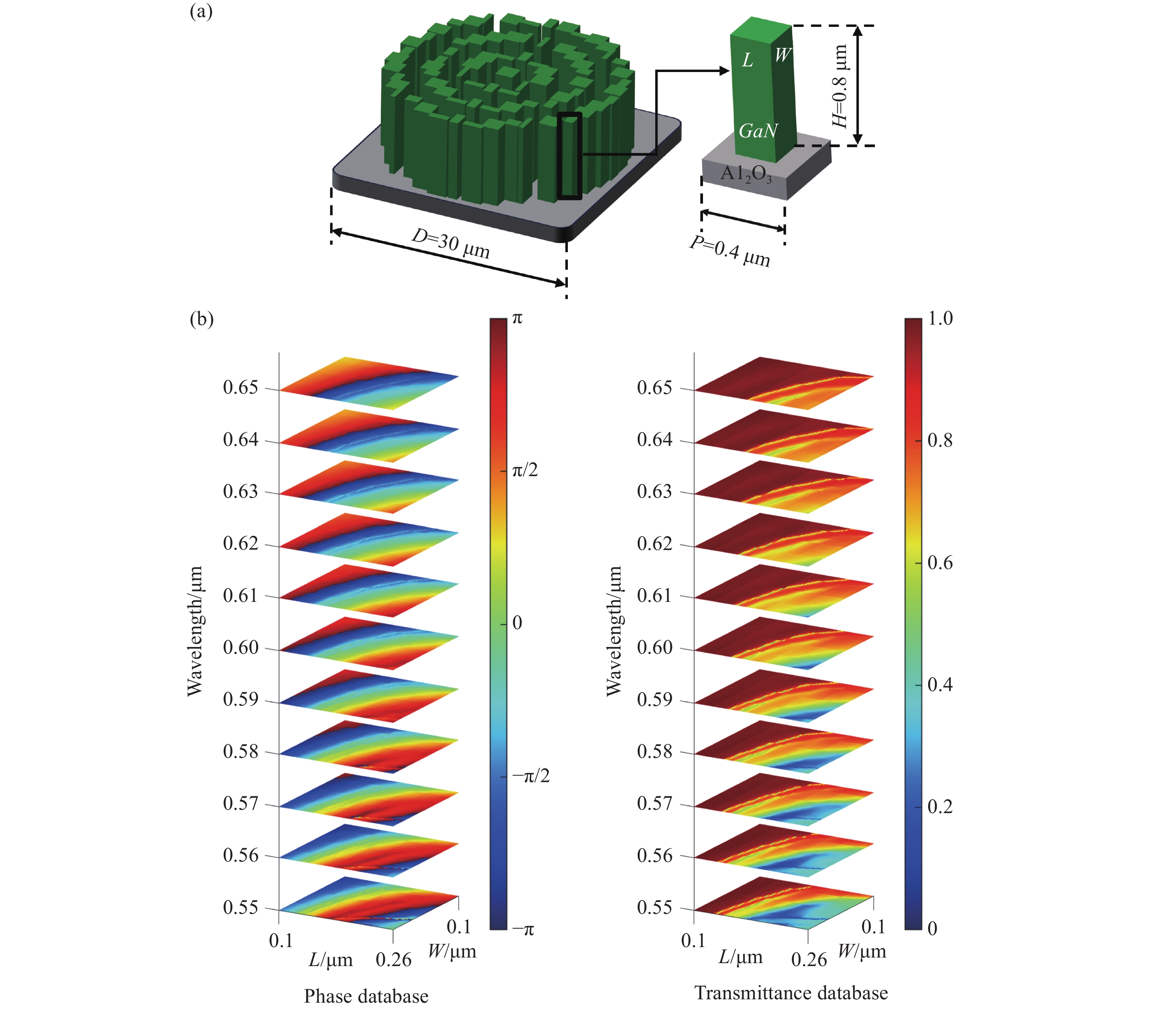
图 4 (a)单元结构示意简图。(b)不同波长下,不同L与W对应的相位与振幅数据库。
Figure 4. (a) Schematic diagram of the unit structure. (b) Phase and transmittance efficiencies as functions of the length L and the width W of the unit structure at different wavelengths.
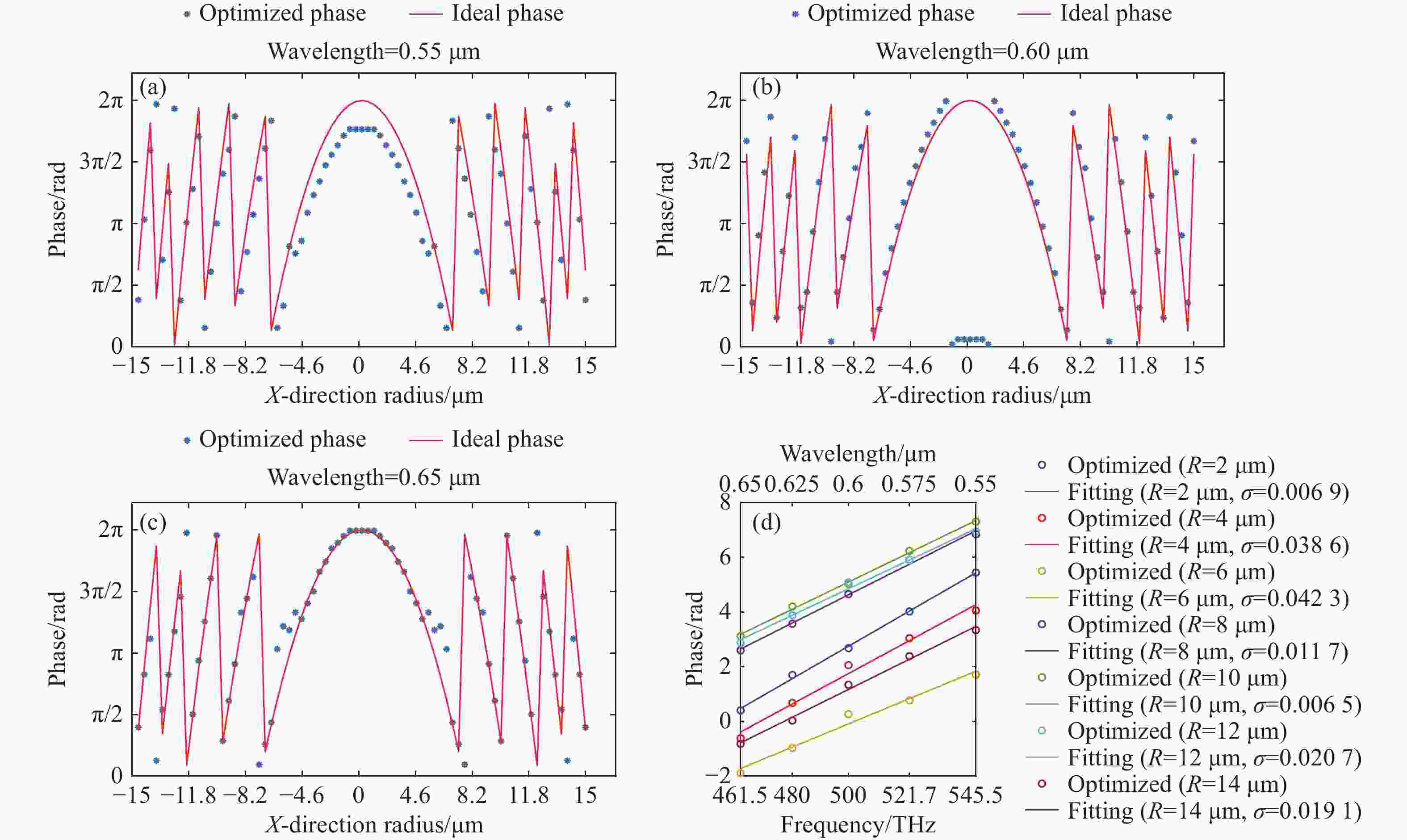
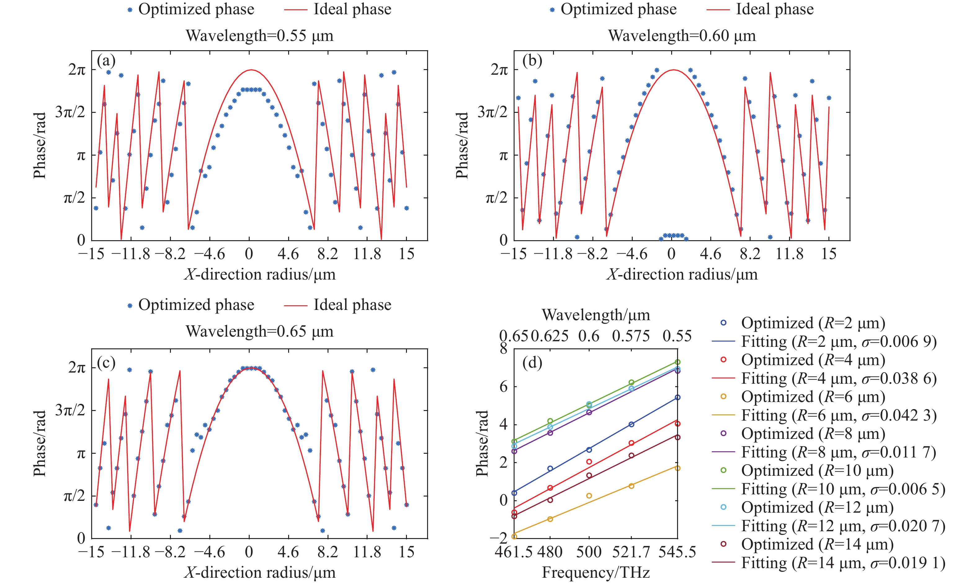
图 5 (a~c) 各优化波长下,消色差超透镜理想相位分布与实际相位分布图。红色实线为理想相位,蓝色散点为实际相位。(d) 超透镜不同位置处的单元结构响应相位随波长变化示意图。其中离散圆点为实际相位,实线为其线性拟合结果。
Figure 5. (a–c) Ideal and optimized phases of the achromatic metalens at each optimized wavelength. The red solid line represents the ideal phase and the blue dots represent the optimized phase. (d) Phases of the unit structure at different positions on the metalens as a function of the wavelength. The discrete dots represent the optimized phases, and the solid lines represent the linear fitting results.
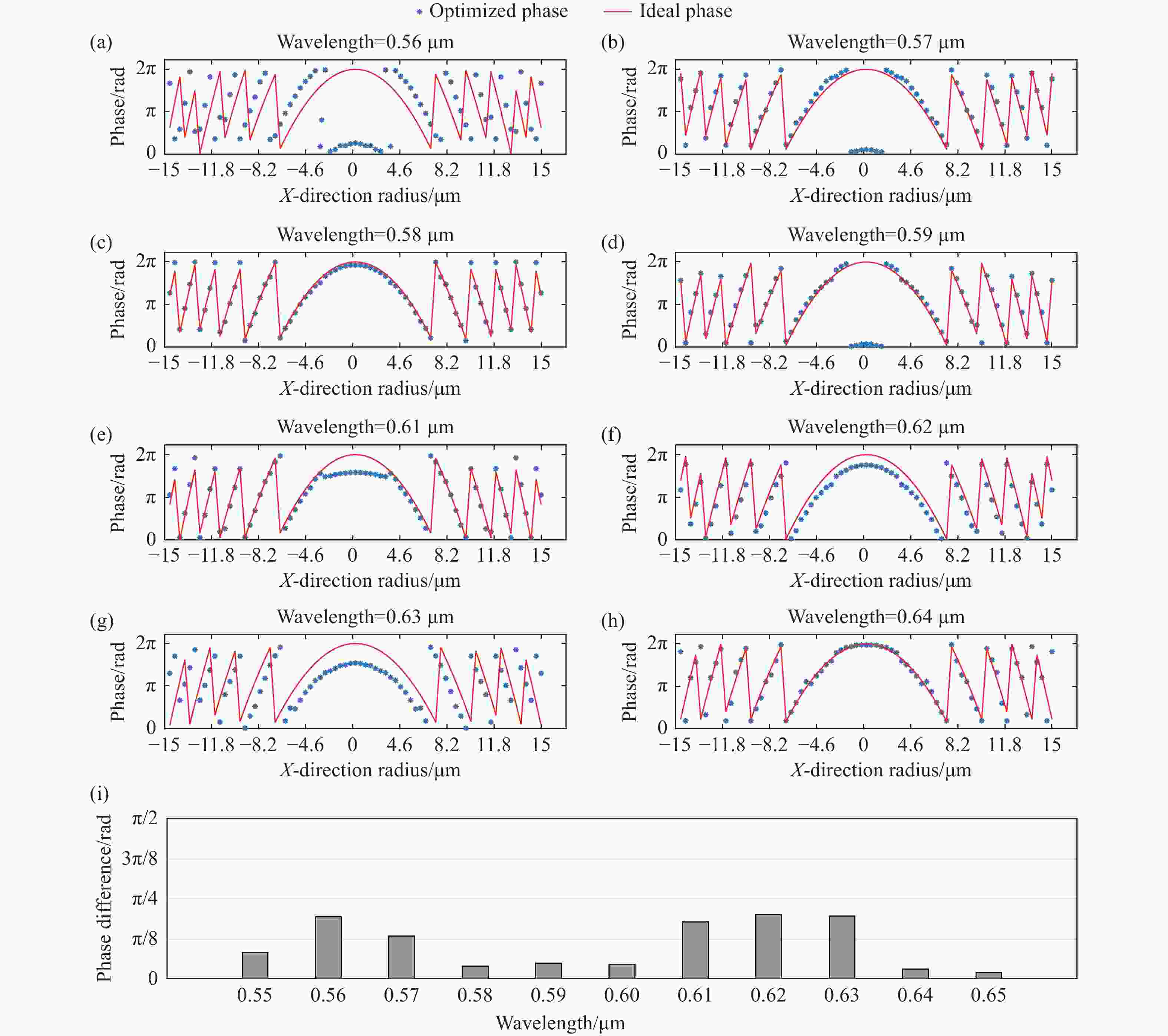
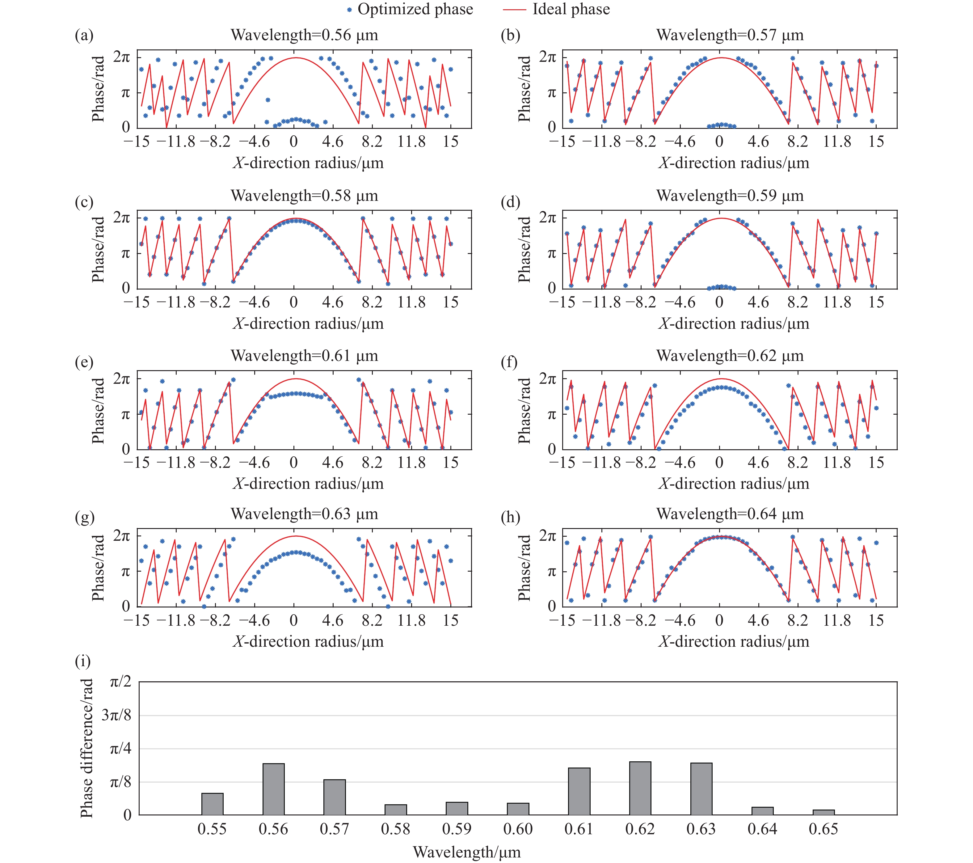
图 6 (a~h) 工作波段内其它波长的理想相位分布与实际相位分布。红色实线为理想相位分布,蓝色散点为实际相位分布。(i) 工作波段内各波长的理想相位与优化之后相位的差值。
Figure 6. (a~h) Ideal and optimized phase distributions at non-optimized wavelengths. The red solid lines represent the ideal phase distributions and the blue dots represent the optimized phase distributions. (i) Differences between the ideal phase and the optimized phase at each wavelength. wavelengths in the working band. The red solid line is the ideal phase distribution and the blue scatter is the actual phase distribution.
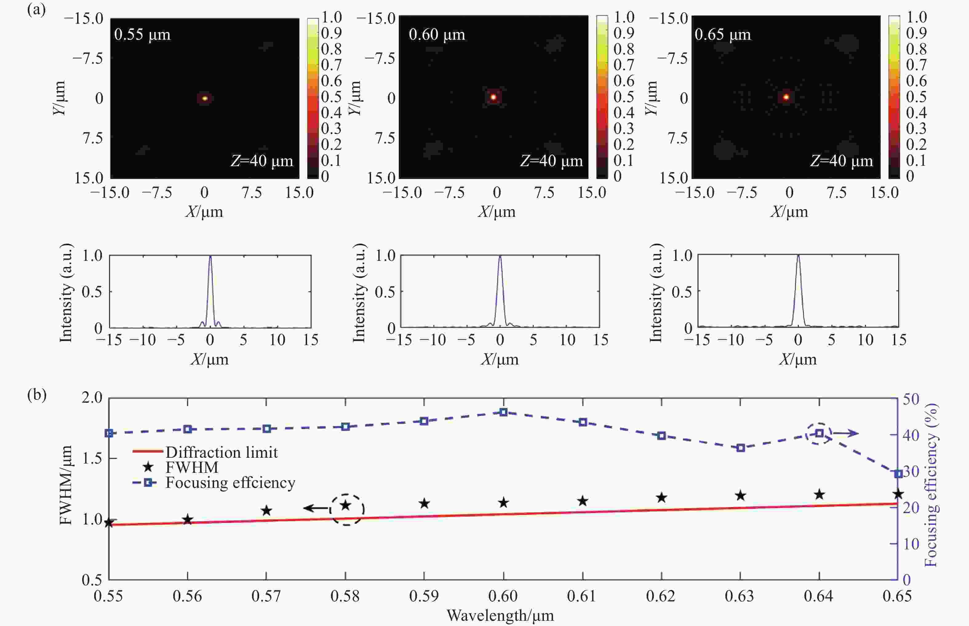
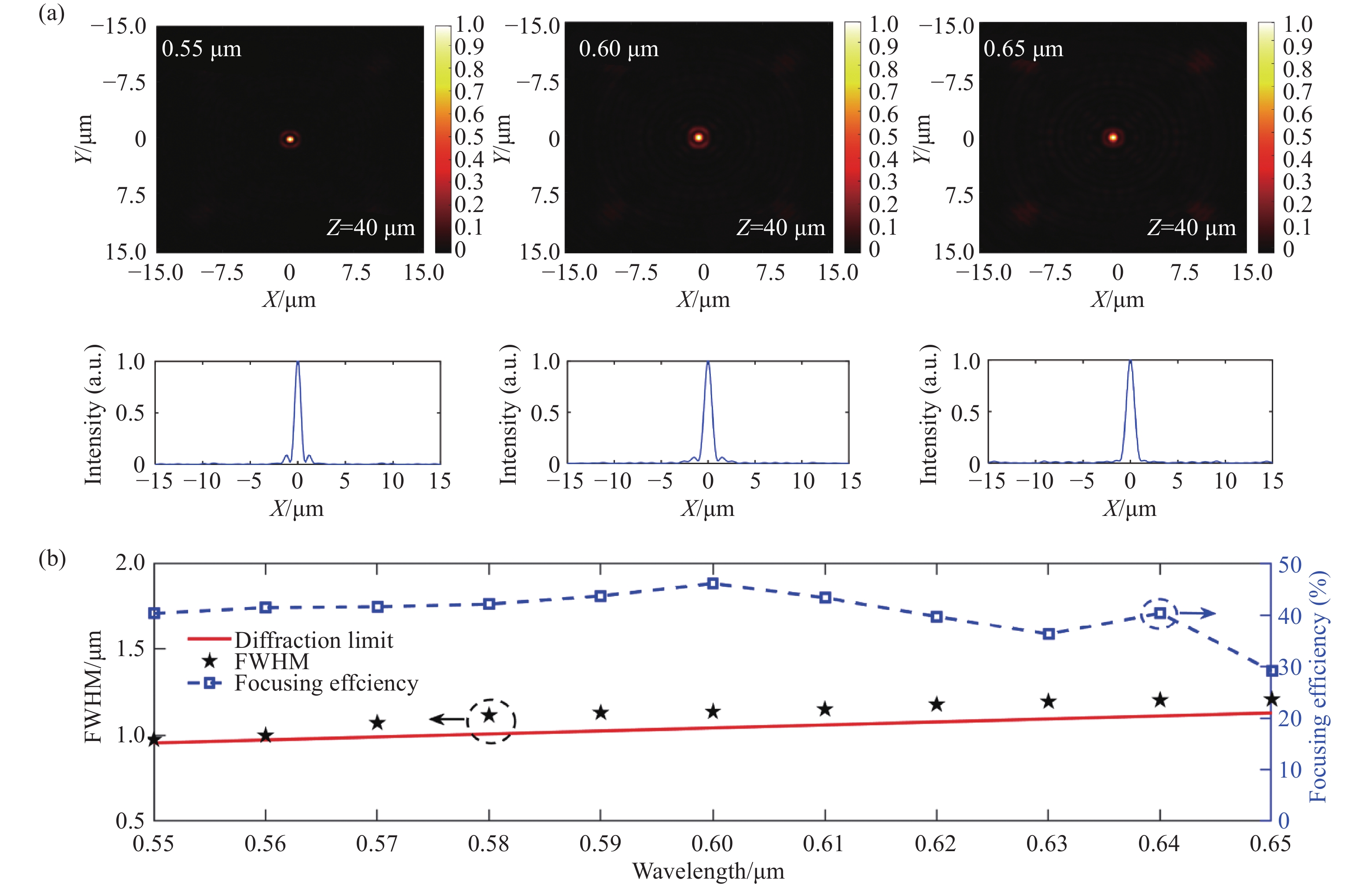
图 7 (a) 各优化波长正入射下,在焦距f0=40 μm处xy平面内聚焦光场强度分布示意图。上半部分表示焦平面在不同波长下的聚焦效果,下半部分表示焦平面处焦斑沿x方向的归一化强度分布。(b) 工作波段内焦斑尺寸及聚焦效率随波长变化示意图。其中黑色五角星代表工作带宽内各波长在z=40 μm处聚焦光斑的FWHM,红色实线为衍射极限,蓝色虚线代表聚焦效率。
Figure 7. (a) Electrical intensity distributions of the focused light field in the xy-plane at the focal length f0 = 40 μm for each of the optimized wavelengths under normal light incidence. The upper parts show the electrical intensity distributions on the focal plane at the different wavelengths, and the lower parts show the corresponding normalized intensity distributions of the focal spot along the x-direction on the focal plane. (b) Focal spot size and focusing efficiency as a function of wavelength within the waveband. The black stars represent the FWHM values of the focal spot at the focal length f0 = 40 μm for each wavelength within the waveband; the red solid line represents the diffraction limit, and the blue dashed line represents the focusing efficiency.

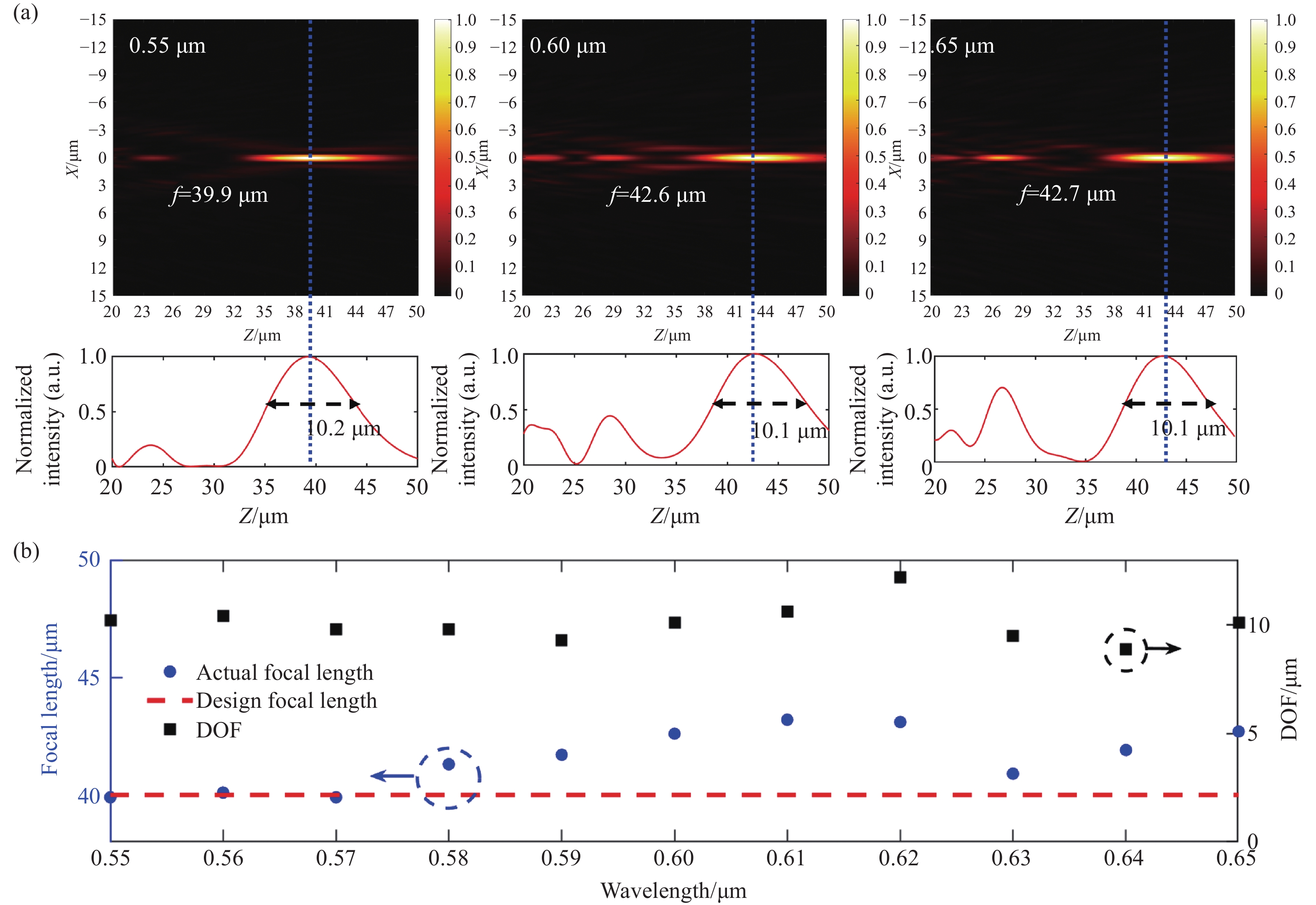
图 8 (a)各优化波长正入射下,xz平面光场强度分布示意图。上半部分是xz平面的光场分布。下半部分是沿z轴的能量归一化强度分布图,图中的黑色双箭头为不同波长下的焦深。(b)工作波段内,超构表面透镜的实际焦距和焦深随波长变化。蓝色圆点表示实际焦距,红色虚线表示预设焦距,黑色方点表示工作波段内各波长的焦深。
Figure 8. (a) Electrical intensity distributions in the xz plane under normal incidence conditions for each optimized wavelength. The upper parts show the electrical intensity distributions in the xz plane. The lower parts show the normalized electrical intensity distributions along the z-axis, and the black double arrows in the figures indicate the focal depths at the different wavelengths. (b) Actual focal length and depth of focus (DOF) as functions of the wavelength. The blue dots indicate the actual focal length values, the red dashed line indicates the focal length f0=40 μm, and the black square dots indicate the DOF values.
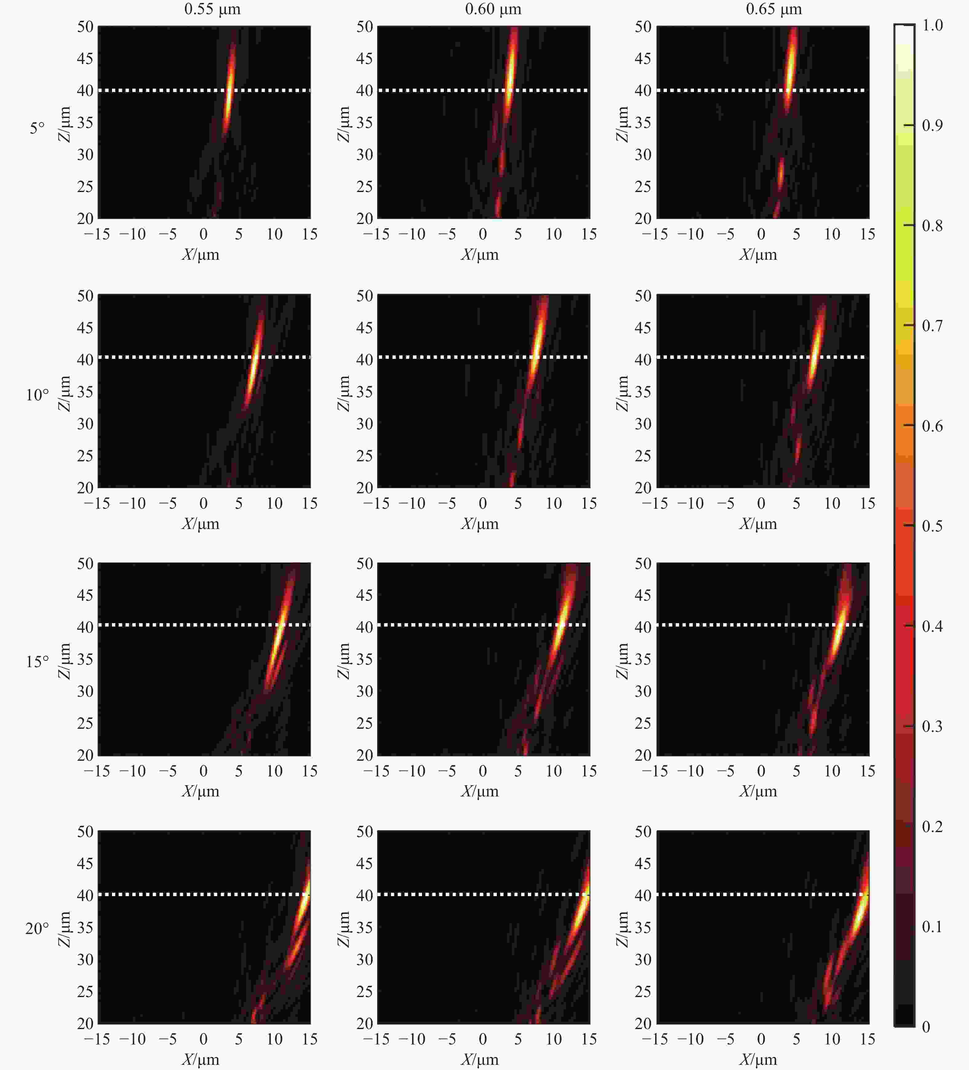
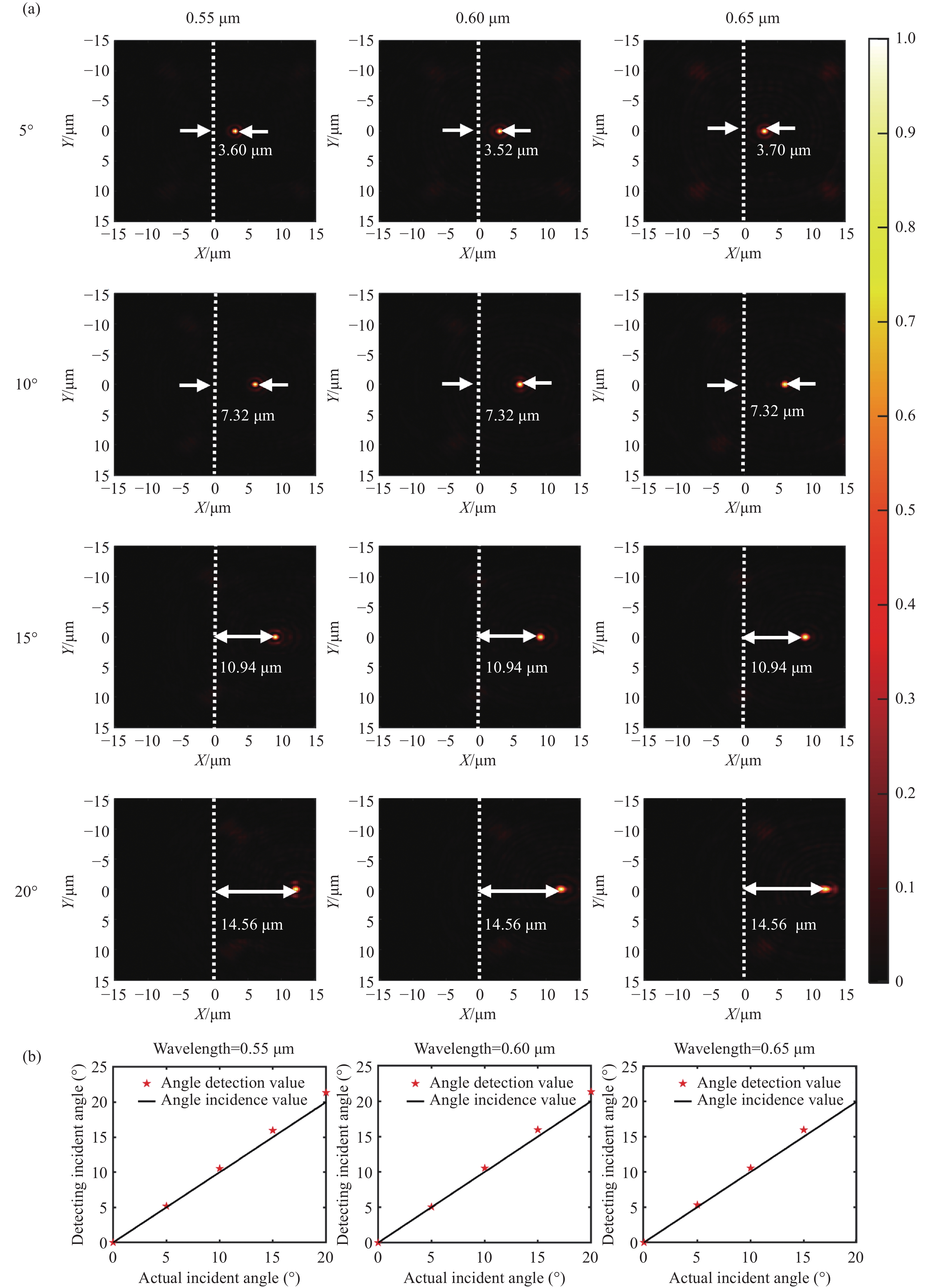
图 9 不同波长下,入射角5°、10°、15°、20°,xz平面内电场归一化强度分布。其中白色虚线为理想焦距f0=40 μm处。
Figure 9. Normalized electrical intensity distributions on the xz plane at angles of incidence of 5°, 10°, 15° and 20°. The white dashed lines indicate the ideal focal length f0 = 40 μm.

图 10 (a)不同波长下,入射角5°、10°、15°、20°,在理想焦距f0=40 um处,xy平面聚焦光场的归一化电场强度分布图。其中白色虚线为焦平面正中位置。(b) 不同波长下,根据焦斑偏移量计算的入射角误差。
Figure 10. (a) Normalized electric intensity distributions on the xy-plane at angles of incidence of 5°, 10°, 15°, and 20° at the ideal focal length f0 = 40 µm. (b) Detected angle of incidence characteristics calculated based on the offset of the focal spot at the different wavelengths.
-
[1] WIRTH-SINGH A, FRÖCH J E, YANG F, et al. Wide field of view large aperture meta-doublet eyepiece[J]. Light: Science & Applications, 2025, 14(1): 17. [2] DENG J, WU K L, FU R, et al. Full-space and wide field-of-view metalens based on 1D photonic crystal[J]. Optics & Laser Technology, 2025, 182: 112187. [3] CHEN CH CH, GU H G, LIU SH Y. Ultra-broadband diffractive imaging with unknown probe spectrum[J]. Light: Science & Applications, 2024, 13(1): 213. [4] PENG Y Y, ZHANG J W, ZHOU X T, et al. Metalens in improving imaging quality: advancements, challenges, and prospects for future display[J]. Laser & Photonics Reviews, 2024, 18(4): 2300731. [5] VALLE P J, CAGIGAL M P. Analytic design of multiple-axis, multifocal diffractive lenses[J]. Optics Letters, 2012, 37(6): 1121-1123. doi: 10.1364/OL.37.001121 [6] HAO Q, TAO X, HU Y, et al. Interferometric measurement of high-order aspheric surface parameter errors based on a virtual-real combination iterative algorithm[J]. Optics Express, 2021, 29(17): 27014-27030. doi: 10.1364/OE.435252 [7] PAN M Y, FU Y F, ZHENG M J, et al. Dielectric metalens for miniaturized imaging systems: progress and challenges[J]. Light: Science & Applications, 2022, 11(1): 195. [8] RUBIN N A, D’AVERSA G, CHEVALIER P, et al. Matrix Fourier optics enables a compact full-Stokes polarization camera[J]. Science, 2019, 365(6448): eaax1839. doi: 10.1126/science.aax1839 [9] ZUO J W, BAI J, CHOI S, et al. Chip-integrated metasurface full-Stokes polarimetric imaging sensor[J]. Light: Science & Applications, 2023, 12(1): 218. [10] ARBABI E, KAMALI S M, ARBABI A, et al. Full-Stokes imaging polarimetry using dielectric metasurfaces[J]. ACS Photonics, 2018, 5(8): 3132-3140. doi: 10.1021/acsphotonics.8b00362 [11] REN Y Z, GUO S H, ZHU W Q, et al. Full‐stokes polarimetry for visible light enabled by an all‐dielectric metasurface[J]. Advanced Photonics Research, 2022, 3(7): 2100373. doi: 10.1002/adpr.202100373 [12] LIU J Y, CHU J K, ZHANG R, et al. Wide field of view and full Stokes polarization imaging using metasurfaces inspired by the stomatopod eye[J]. Nanophotonics, 2023, 12(6): 1137-1146. doi: 10.1515/nanoph-2022-0712 [13] KHORASANINEJAD M, CHEN W T, ZHU A Y, et al. Multispectral chiral imaging with a metalens[J]. Nano Letters, 2016, 16(7): 4595-4600. doi: 10.1021/acs.nanolett.6b01897 [14] ENGAY E, HUO D W, MALUREANU R, et al. Polarization-dependent all-dielectric metasurface for single-shot quantitative phase imaging[J]. Nano Letters, 2021, 21(9): 3820-3826. doi: 10.1021/acs.nanolett.1c00190 [15] . YANG Y, SEONG J, CHOI M, et al. Integrated metasurfaces for re-envisioning a near-future disruptive optical platform[J]. Light: Science & Applications, 2023, 12(1): 152. [16] LIU R, LI W H, ZHANG W, et al. Manipulating continuous optical spectra in the wave vector domain by metalens[J]. Optics Letters, 2025, 50(2): 598-601. doi: 10.1364/OL.544925 [17] SHRESTHA S, OVERVIG A C, LU M, et al. Broadband achromatic dielectric metalenses[J]. Light: Science & Applications, 2018, 7(1): 85. [18] SUN T, HU J P, ZHU X J, et al. Broadband single‐chip full stokes polarization‐spectral imaging based on all‐dielectric spatial multiplexing metalens[J]. Laser & Photonics Reviews, 2022, 16(6): 2100650. [19] CHEN W T, ZHU A Y, SISLER J, et al. Broadband achromatic metasurface-refractive optics[J]. Nano Letters, 2018, 18(12): 7801-7808. doi: 10.1021/acs.nanolett.8b03567 [20] ZHANG F, PU M B, LI X, et al. Extreme‐angle silicon infrared optics enabled by streamlined surfaces[J]. Advanced Materials, 2021, 33(11): 2008157. doi: 10.1002/adma.202008157 [21] . WANG J L, DENG Y T, WANG CH M, et al. Portable astronomical observation system based on large-aperture concentric-ring metalens[J]. Light: Science & Applications, 2025, 14(1): 2. [22] BARANIKOV A V, KHAIDAROV E, LASSALLE E, et al. Large field‐of‐view and multi‐color imaging with GaP quadratic metalenses[J]. Laser & Photonics Reviews, 2024, 18(1): 2300553. [23] KHORASANINEJAD M, SHI Z, ZHU A Y, et al. Achromatic metalens over 60 nm bandwidth in the visible and metalens with reverse chromatic dispersion[J]. Nano Letters, 2017, 17(3): 1819-1824. doi: 10.1021/acs.nanolett.6b05137 [24] WANG SH M, WU P C, SU V C, et al. A broadband achromatic metalens in the visible[J]. Nature Nanotechnology, 2018, 13(3): 227-232. doi: 10.1038/s41565-017-0052-4 [25] CHEN W T, ZHU A Y, SANJEEV V, et al. A broadband achromatic metalens for focusing and imaging in the visible[J]. Nature Nanotechnology, 2018, 13(3): 220-226. doi: 10.1038/s41565-017-0034-6 [26] ZHANG Y X, JIN J J, PU M B, et al. Full stokes polarimetry for wide‐angle incident light[J]. Physica Status Solidi (RRL)–Rapid Research Letters, 2020, 14(5): 2000044. doi: 10.1002/pssr.202000044 [27] LIU S J, ZHANG Z J, CHENG J X, et al. Design of full stokes vector polarimetry based on metasurfaces for wide-angle incident light[J]. Photonics, 2023, 10(4): 382. doi: 10.3390/photonics10040382 [28] GROEVER B, CHEN W T, CAPASSO F. Meta-lens doublet in the visible region[J]. Nano Letters, 2017, 17(8): 4902-4907. doi: 10.1021/acs.nanolett.7b01888 [29] HUANG ZH Y, QIN M S, GUO X W, et al. Achromatic and wide-field metalens in the visible region[J]. Optics Express, 2021, 29(9): 13542-13551. doi: 10.1364/OE.422126 [30] PU M B, LI X, GUO Y H, et al. Nanoapertures with ordered rotations: symmetry transformation and wide-angle flat lensing[J]. Optics Express, 2017, 25(25): 31471-31477. doi: 10.1364/OE.25.031471 [31] VAN DEN BOS A. Rayleigh wave-front criterion: comment[J]. Journal of the Optical Society of America A, 1999, 16(9): 2307-2309. doi: 10.1364/JOSAA.16.002307 [32] ZHAO Y N, CHEN CH, ZHONG X, et al. Enhancing OFDM with index modulation using heuristic geometric constellation shaping and generalized interleaving for underwater VLC[J]. Optics Express, 2024, 32(8): 13720-13732. doi: 10.1364/OE.521045 [33] ZHANG CH, CHEN M SH, ZHANG L R, et al. Broadband achromatic metalens design based on predictive neural network and particle swarm optimization-genetic algorithm[J]. New Journal of Physics, 2023, 25(10): 103040. doi: 10.1088/1367-2630/ad02dc [34] WANG SH M, WU P C, SU V C, et al. Broadband achromatic optical metasurface devices[J]. Nature Communications, 2017, 8(1): 187. doi: 10.1038/s41467-017-00166-7 -

 下载:
下载:


计量
- 文章访问数: 64
- HTML全文浏览量: 21
- PDF下载量: 8
- 被引次数: 0
