


Investigation of laser-induced damage mechanisms in back-illuminated cmos detector modules under nanosecond pulsed irradiation
-
摘要:
为了模拟真实工作场景下激光对可见光成像系统损伤效应,将滤光片和背照式CMOS探测器共同构成探测器组件作为靶材,探讨两种不同波长的纳秒脉冲激光对探测器组件的损伤效应。首先,通过实验的方式获得532 nm及
1064 nm纳秒脉冲激光对CMOS组件的典型损伤效应数据。然后,利用有限元仿真方法建立激光与探测器相互作用的模型,以解决实验中无法实时观测探测器内部的温度与应力变化和分布的问题,在获得损伤效应数据的同时将传统实验难以观察的温度/应力集中现象“可视化”,提供可靠的参考阈值数据。通过仿真及实验研究表明损伤机理为热-力联合损伤,并得了如下的损伤阈值,532 nm波段下各阶段损伤阈值为30.06 mJ/cm2、38.93 mJ/cm2、56.20 mJ/cm2和102.17 mJ/cm2,1064 nm波段下为38.62 mJ/cm2、50.09 mJ/cm2、116.31 mJ/cm2和137.73 mJ/cm2。-
关键词:
- 背照式COMS探测器 /
- 纳秒脉冲激光 /
- 激光辐照效应 /
- 损伤机理
Abstract:To evaluate the laser-induced damage effects on visible-light imaging systems under realistic operational conditions, a detector module comprising a filter and a back-illuminated CMOS sensor was employed as the target. This study investigates the damage mechanisms induced by nanosecond pulsed lasers at wavelengths of 532 nm and
1064 nm. Initially, a series of experiments were conducted to characterize the typical damage behaviors resulting from laser irradiation. To address the limitations in observing internal thermal and mechanical responses during the experiments, a finite element simulation model was developed to analyze the interaction between the laser and the detector. The simulation enabled visualization of temperature and stress concentration phenomena that are difficult to capture through direct observation, thus providing valuable reference data for damage thresholds. The results from both the experiments and simulations indicate that the dominant damage mechanism is coupled thermo-mechanical failure. The measured multi-stage damage thresholds were 30.06 mJ/cm2, 38.93 mJ/cm2, 56.20 mJ/cm2, and 102.17 mJ/cm2 for 532 nm laser irradiation, and 38.62 mJ/cm2, 50.09 mJ/cm2, 116.31 mJ/cm2, and 137.73 mJ/cm2 for1064 nm irradiation. -
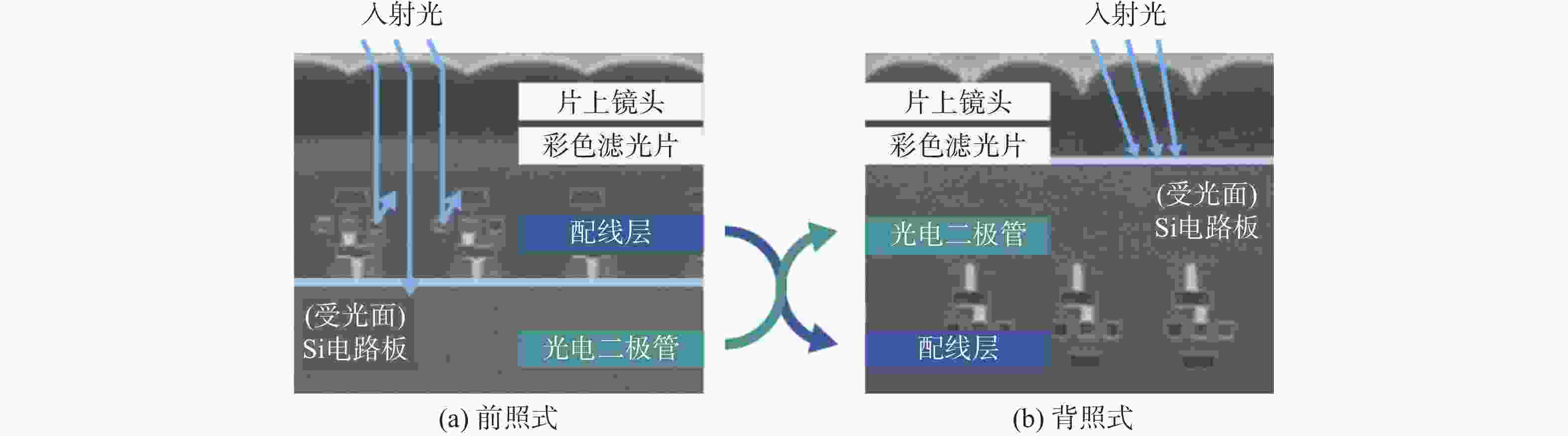
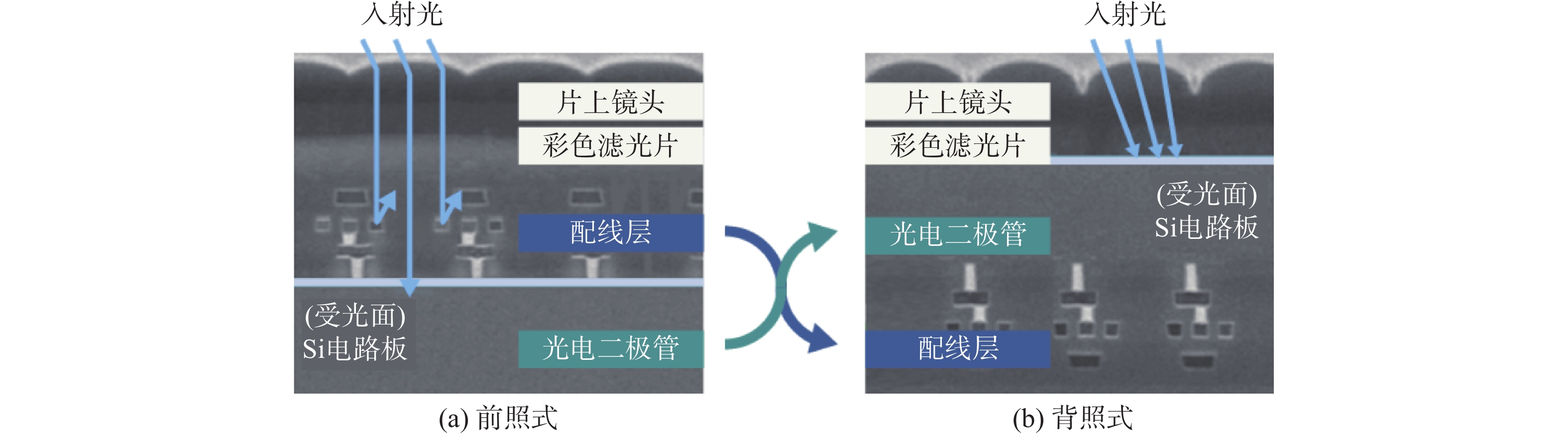
图 1 CMOS探测器基本结构示意图
Figure 1. Schematic Diagram of the Basic Structure of a CMOS Detector

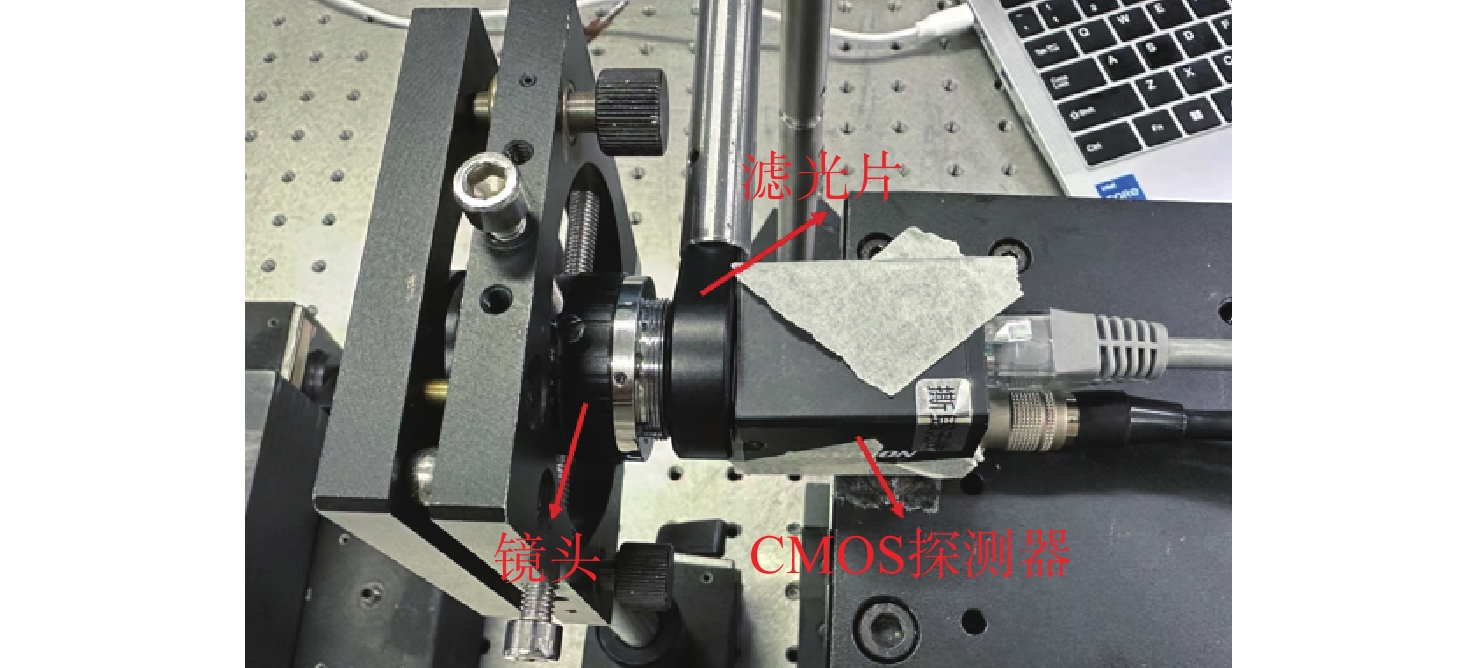
图 2 脉冲激光辐照探测器组件实验原理
Figure 2. Principle of pulsed laser irradiation experiments on detector assemblies
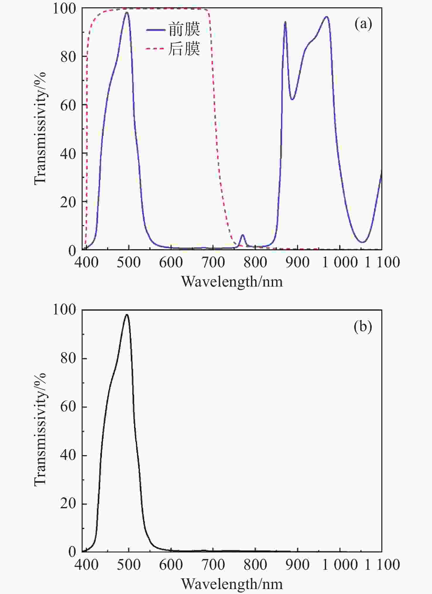
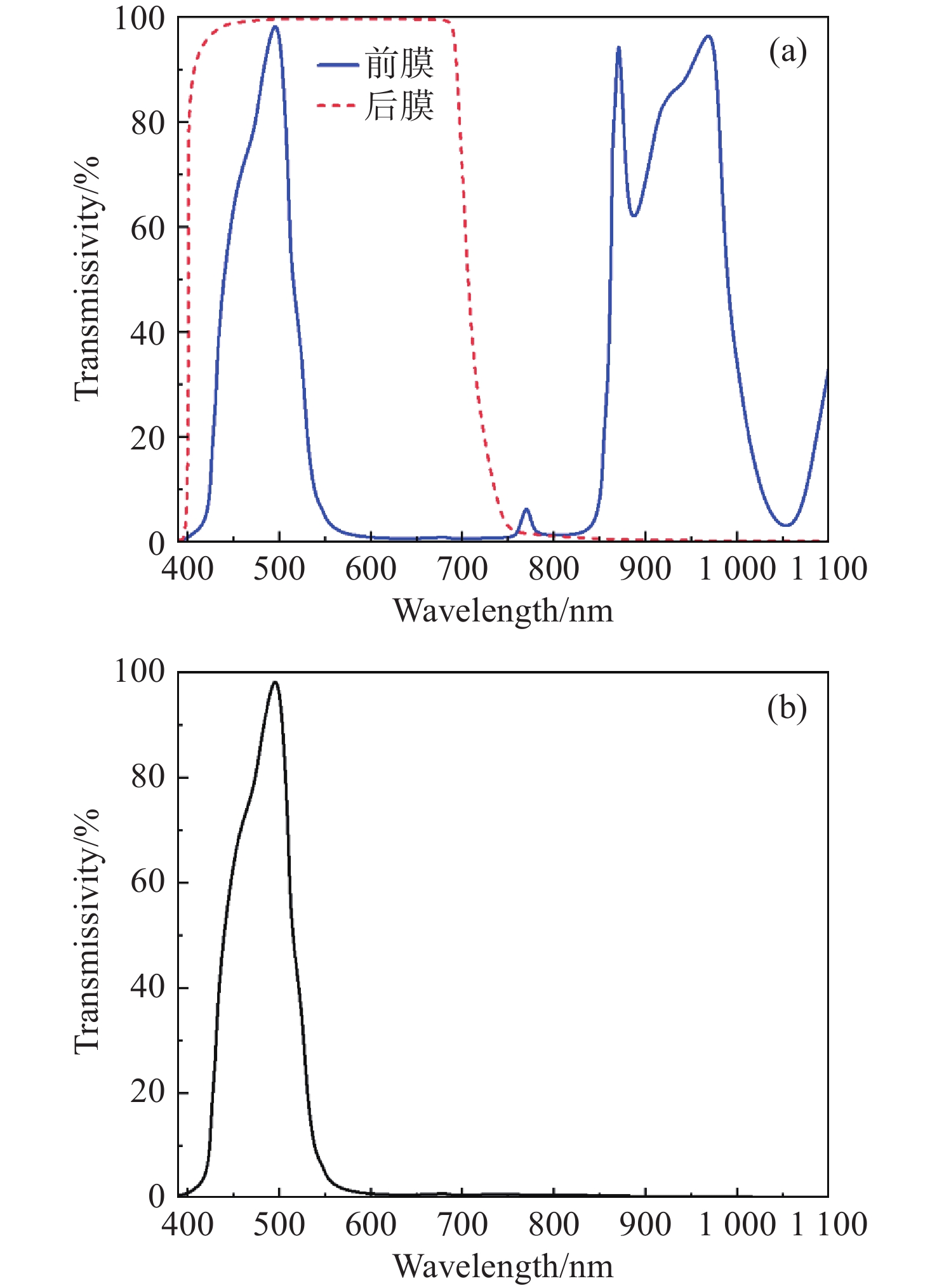
图 4 滤光片光谱曲线 (a) 为前膜和后膜各自光谱曲线, (b) 为前膜和后膜组合光谱曲线
Figure 4. Spectral curve of the filter (a) spectral curves of front and rear films, (b) spectral curve of front film and rear film combination)
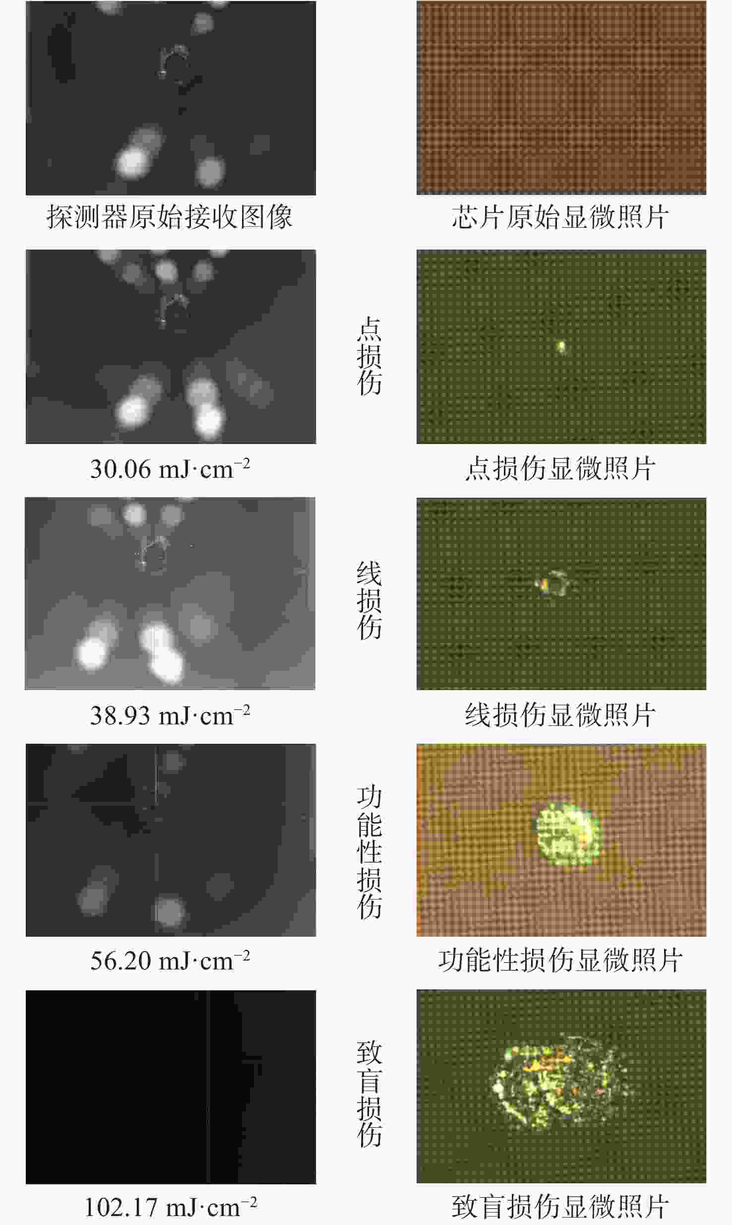
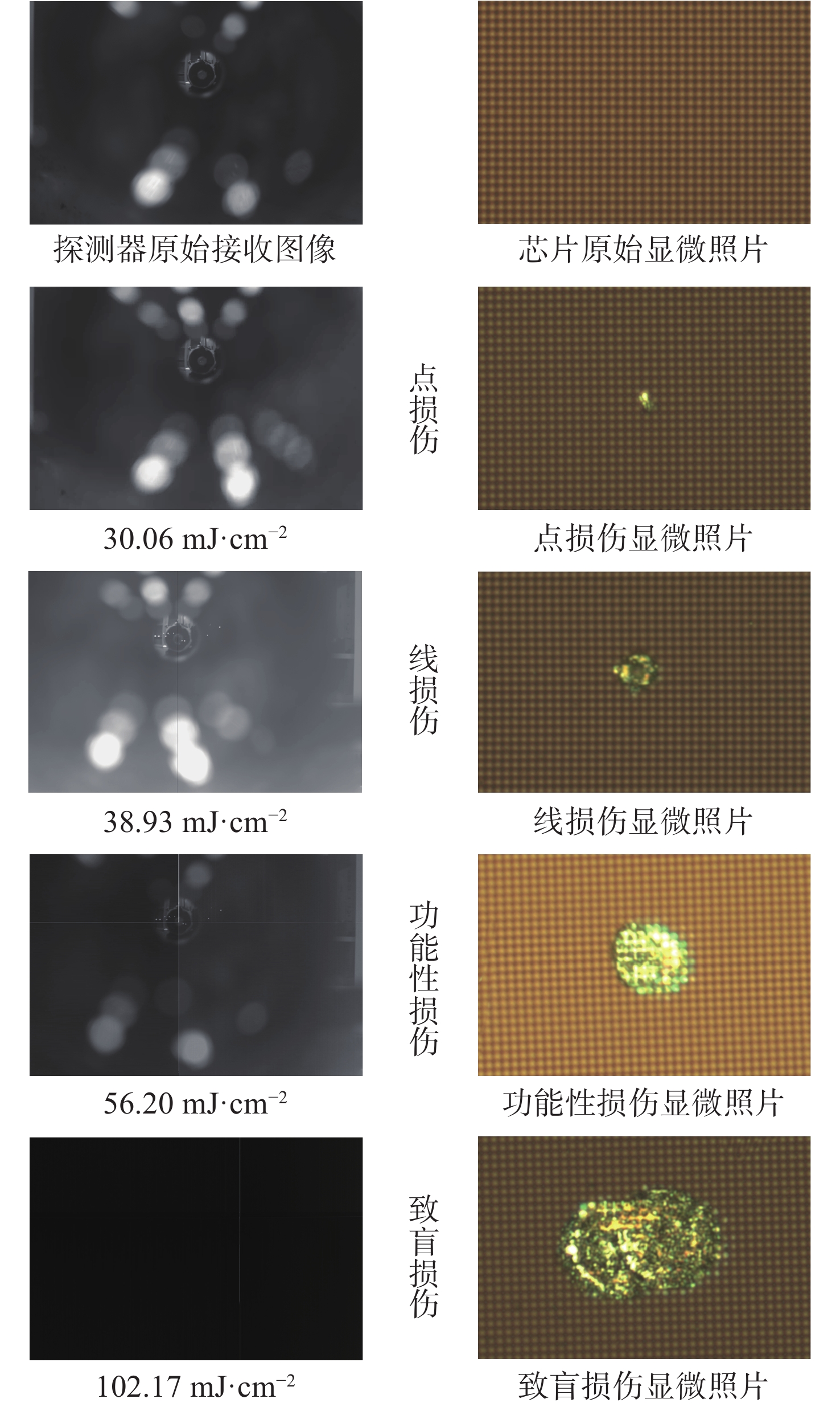
图 5 532 nm纳秒激光辐照后,不同损伤程度的探测器接收图像和芯片损伤形貌
Figure 5. Detector images and chip damage morphology at different damage levels after 532 nm nanosecond laser irradiation
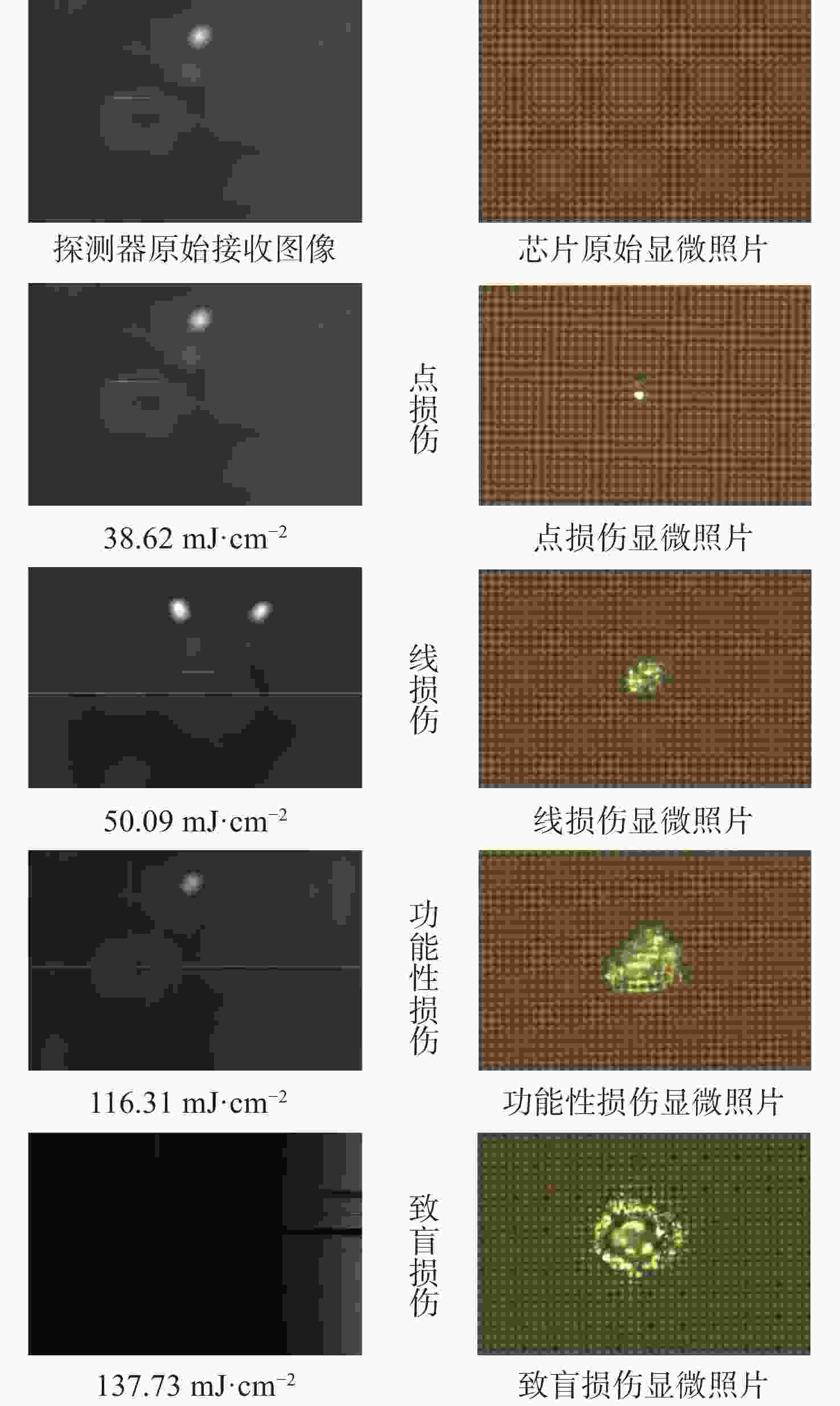
图 6
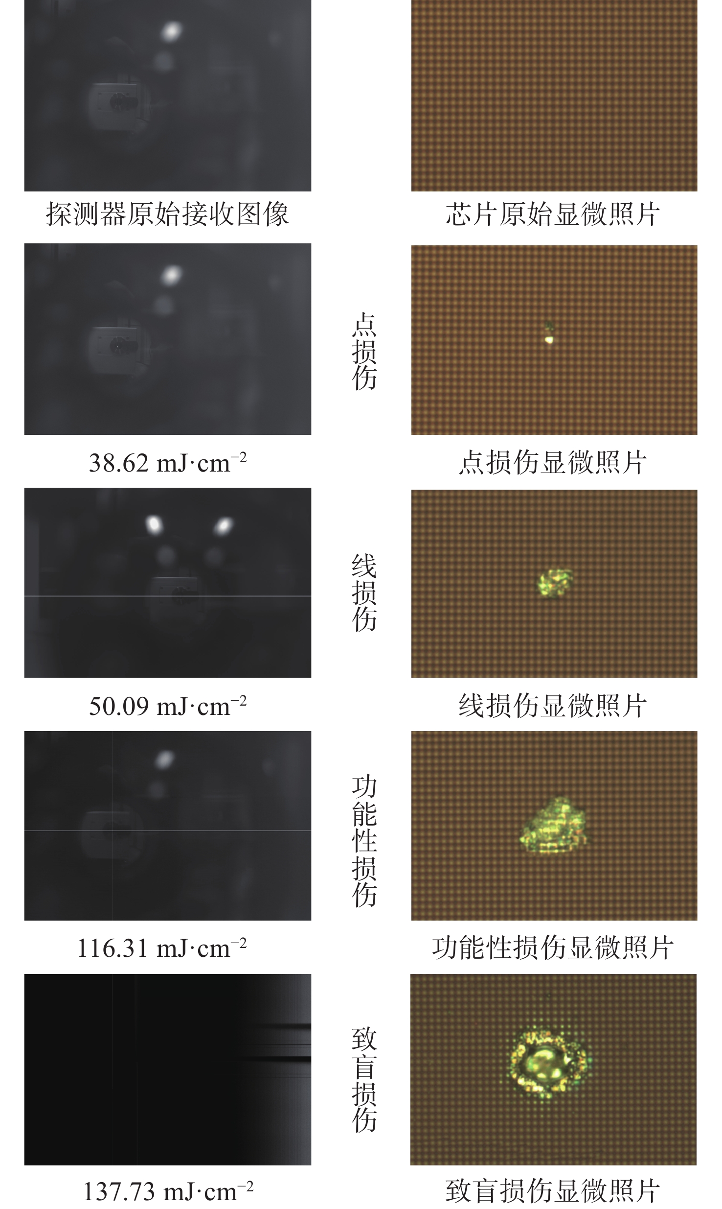
1064 nm纳秒激光辐照后,不同损伤程度的探测器接收图像和芯片损伤形貌Figure 6. Detector images and chip damage morphology at different damage levels after
1064 nm nanosecond laser irradiation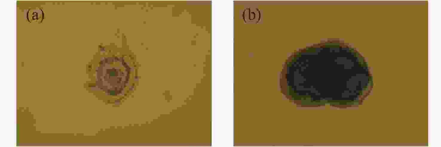
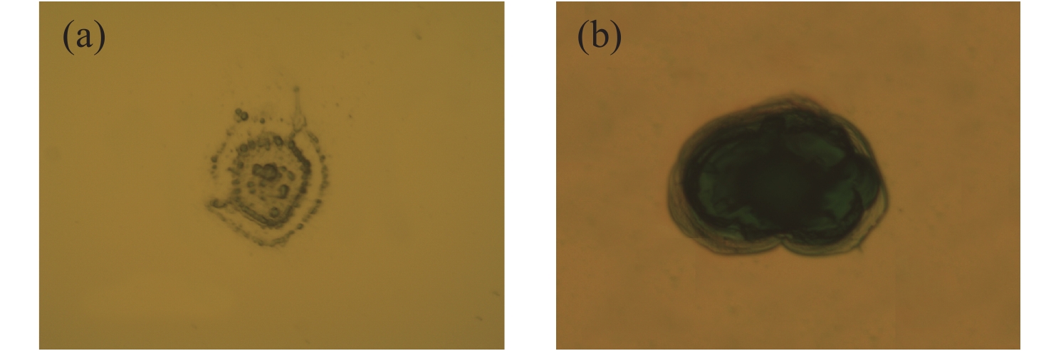
图 7 探测器组件损伤实验得到的滤光片损伤形貌
Figure 7. Damage morphology of the filter obtained from the detector component damage experiment
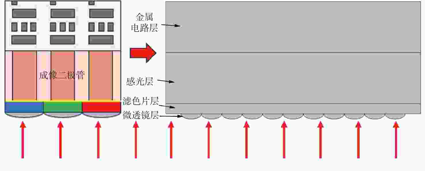
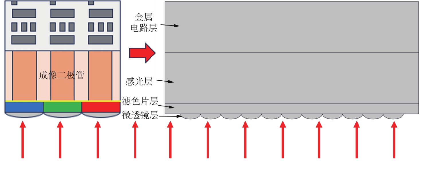
图 8 背照式CMOS探测器二维简化示意图
Figure 8. Simplified two-dimensional schematic of a back-illuminated CMOS detector
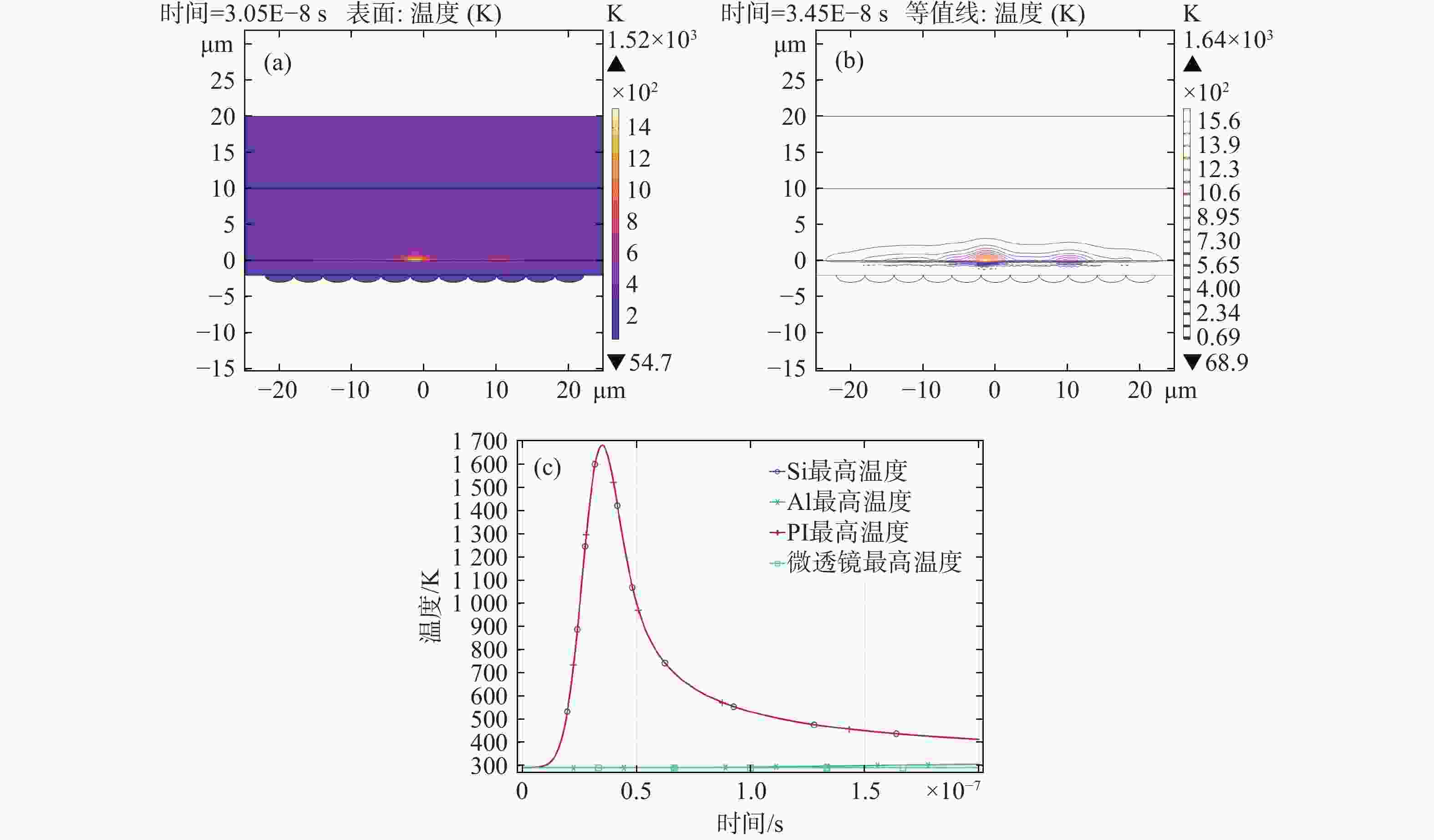
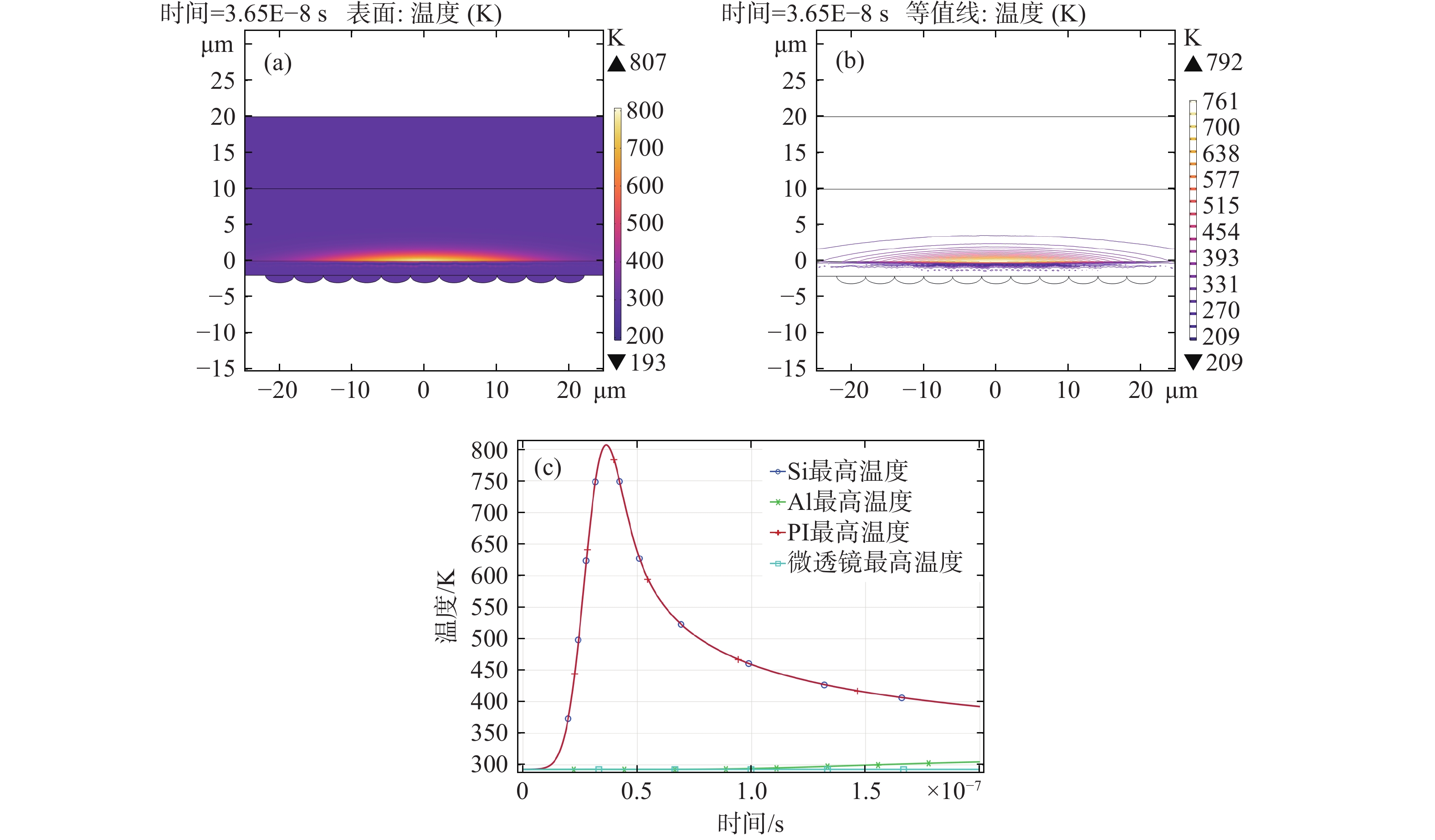
图 9 532 nm纳秒脉冲激光损伤CMOS探测器仿真结果。(a) 最高温度分布图;(b) 最高温度等温线图;(c) 各层最高温度曲线
Figure 9. Simulation results of CMOS detector damage by 532 nm nanosecond pulse laser. (a) Maximum temperature distribution; (b) Isothermal map of maximum temperature; (c) Maximum temperature curves for each layer

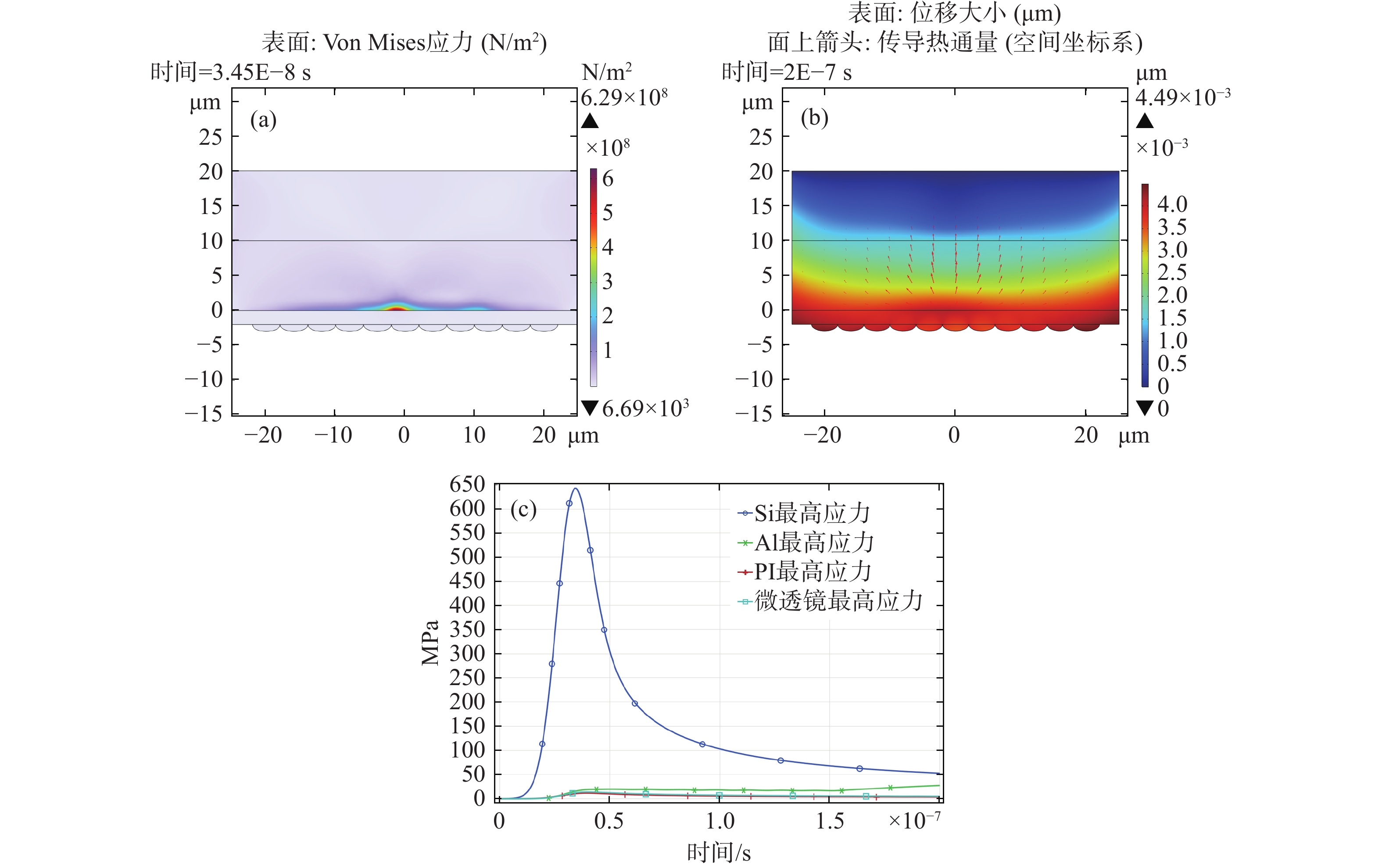
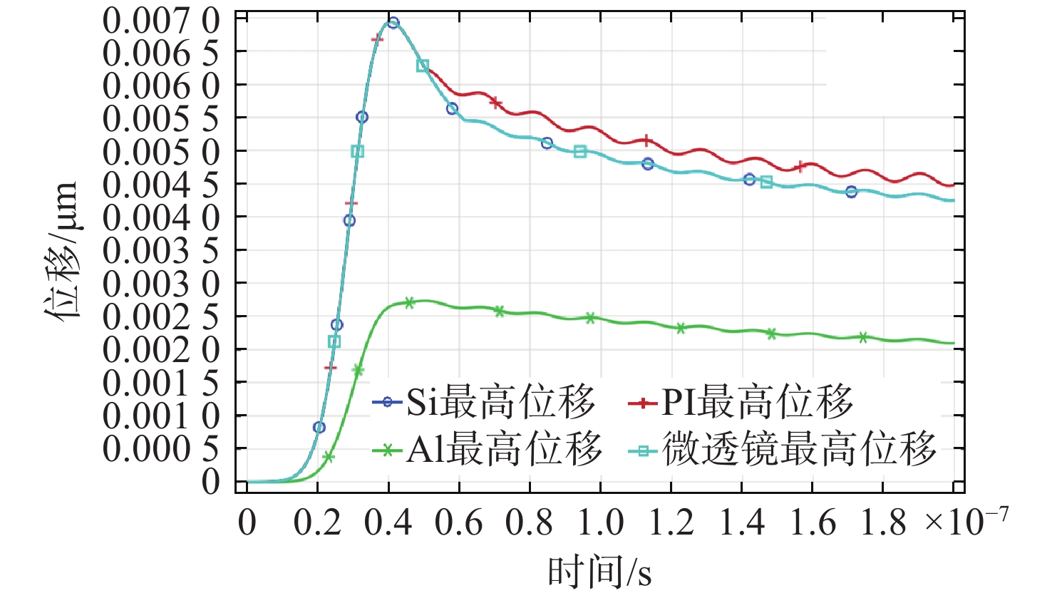
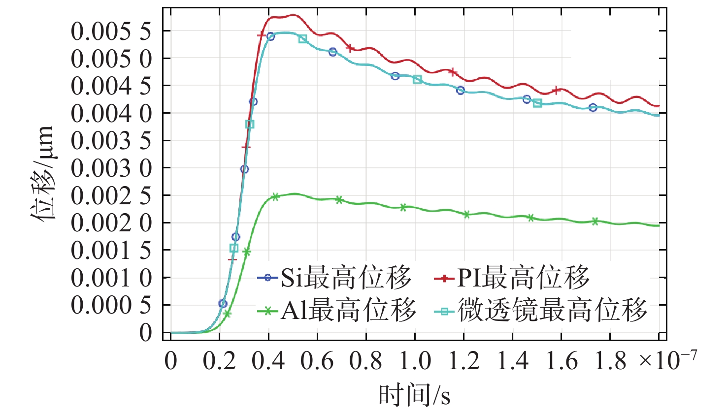
图 10 532 nm激光损伤CMOS探测器应力应变仿真结果。(a)最高应力分布图;(b)最高位移分布图;(c)各层最高应力曲线
Figure 10. Stress-strain simulation results of CMOS detector damage by 532 nm laser. (a) Maximum stress distribution; (b) Maximum displacement distribution; (c) Maximum stress curves for each layer
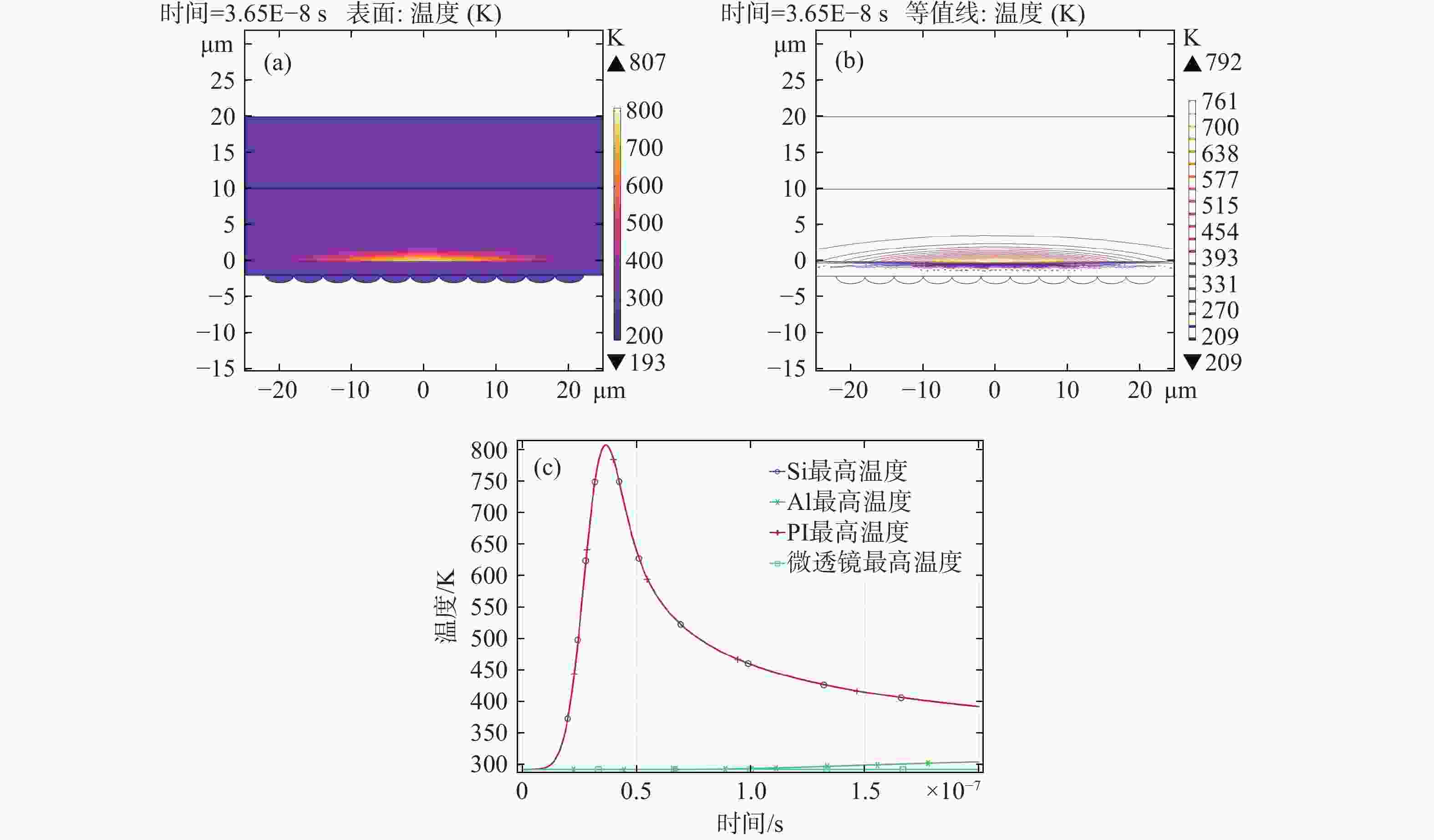
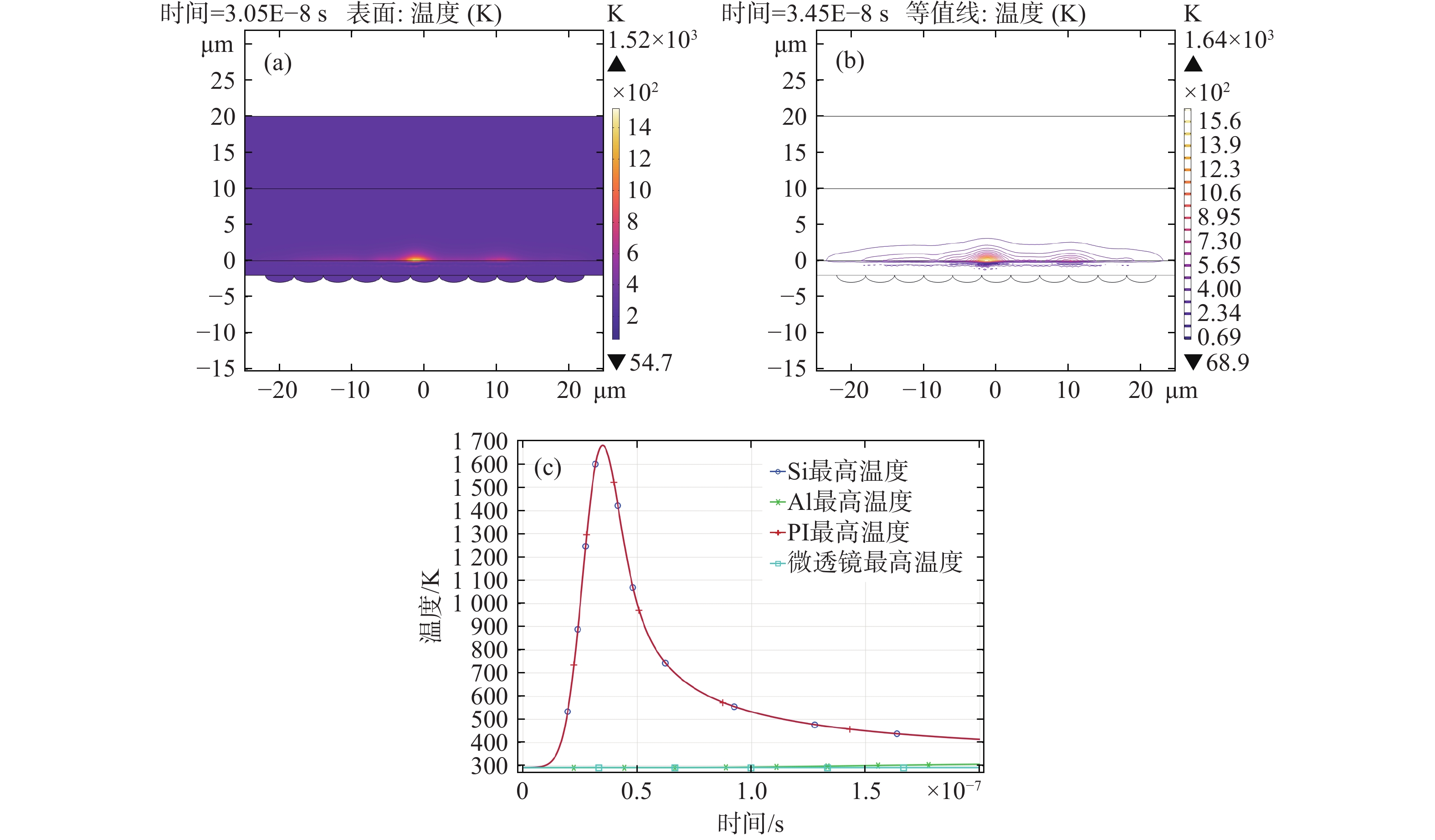
图 12
1064 nm纳秒脉冲激光损伤CMOS探测器仿真结果。(a) 最高温度分布图;(b) 最高温度等温线图;(c) 各层最高温度曲线Figure 12. Simulation results of CMOS detector damage by
1064 nm nanosecond pulse laser. (a) Maximum temperature distribution; (b) Isothermal map of maximum temperature; (c) Maximum temperature curves for each layer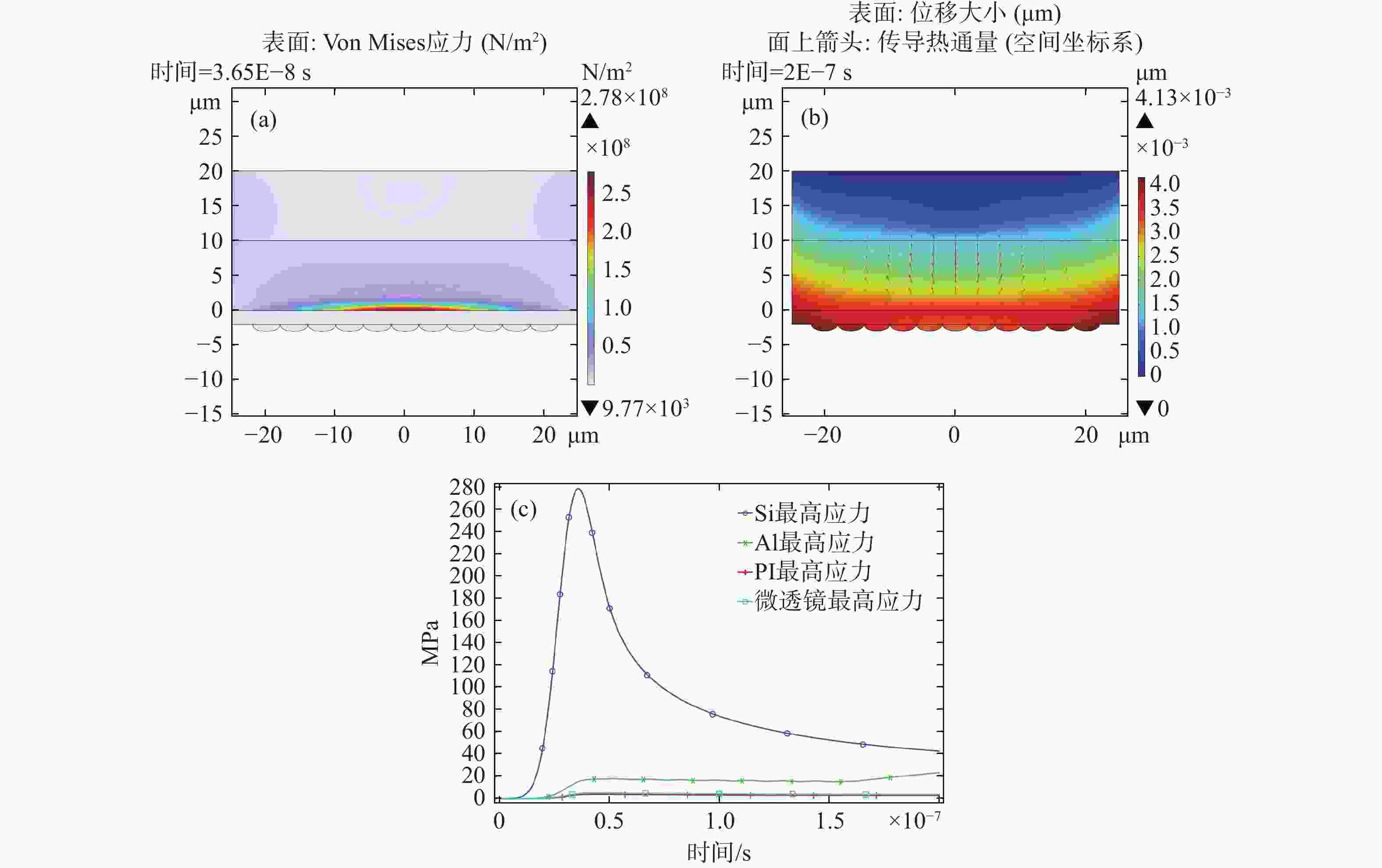
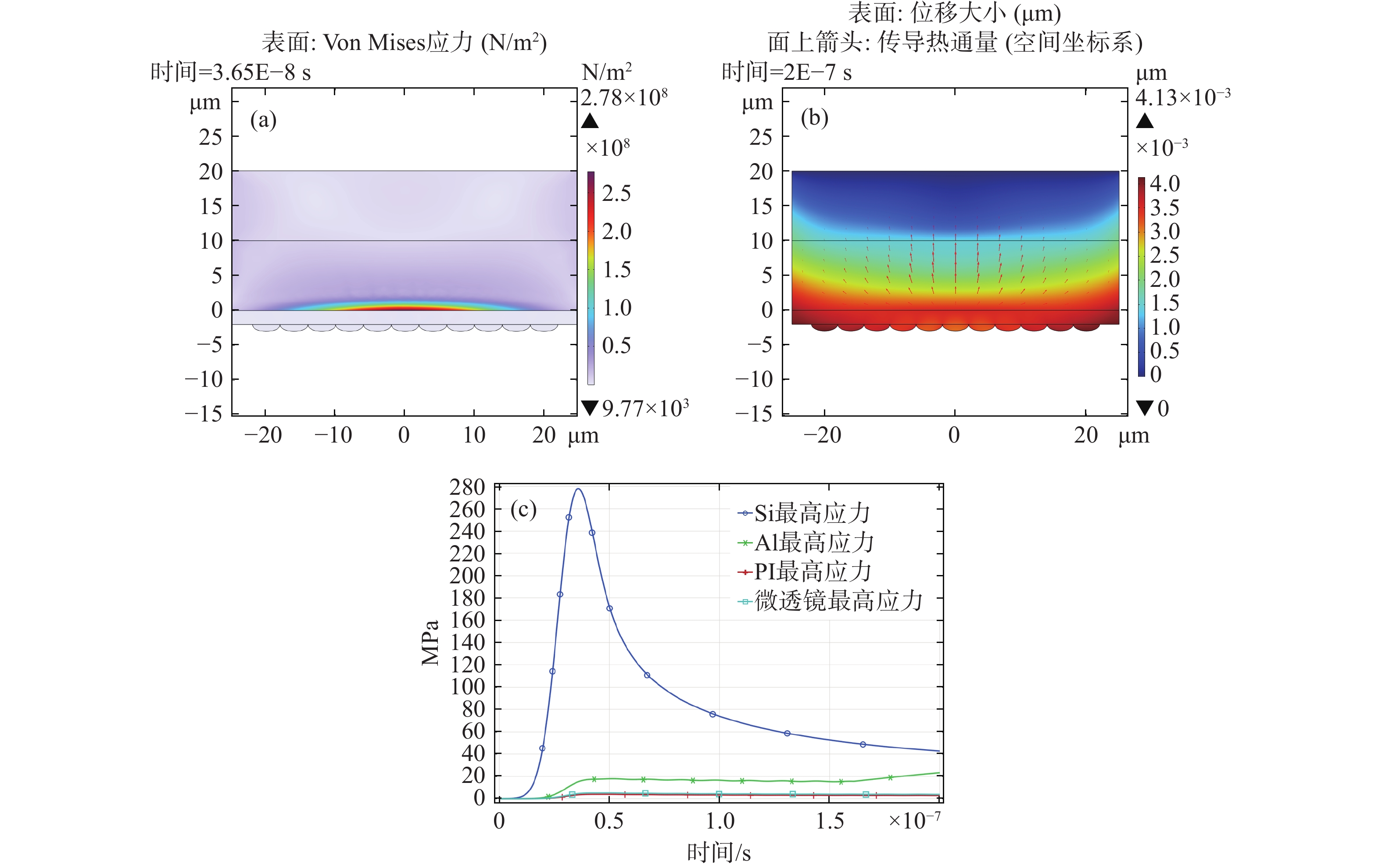
图 13
1064 nm激光损伤CMOS探测器应力应变仿真结果。(a) 最高应力分布图;(b) 最高位移分布图;(c) 各层最高应力曲线Figure 13. Stress-strain simulation results of CMOS detector damage by
1064 nm laser. (a) Maximum stress distribution; (b) Maximum displacement distribution; (c) Maximum stress curves for each layer表 1 激光对光电载荷探测器组件的损伤实验主要设备
Table 1. Main Experimental Equipment for Laser-Induced Damage Testing on Electro-Optical Payload Detector Assemblies
设备名称 设备型号 设备参数 激光器 Nimma-900 单脉冲<900 mJ 波长532/ 1064 nm
脉宽9 ns能量计 Ophir PD-10 测量范围1 nJ~13 μJ Ophir PE-50 测量范围10 μJ~10 J 格兰棱镜
L2大恒GCL-070210 工作波长350− 2500 nm;通光孔径
10 mm;消光比105∶1半波片L1 大恒GCL-060512 工作波长532 nm;透过率T>98% 大恒GCL-060517 工作波长1064nm;透过率T>98% 扩束器 自研定制 工作波长532 nm 扩束倍数4× LBTEK BEF03-B 工作波段650~ 1100 nm 扩束倍数3× 下载: 导出CSV
表 2 海康威视MV-CA060-11GM基本参数
Table 2. Basic specifications of the Hikvision MV-CA060-11GM
参数 海康威视MV-CA060-11GM 传感器类型 CMOS,卷帘快门 传感器型号 Sony IMX178 像元尺寸 2.4 μm × 2.4 μm 最大帧率 17 fps 分辨率 3072 ×2048增益 0 dB~20 dB 曝光时间 27 μs~2.5 sec
下载: 导出CSV
表 3 海康威视MV-CA060-11GM基本参数
Table 3. Basic specifications of the Hikvision MV-CA060-11GM
PI Si Al 恒压热容 J/(kg·K) 1510 700 900 密度 kg/m³ 1190 2329 2700 导热系数 W/(m·K) 0.3 130 238 杨氏模量 Pa 3.2×10⁹ 1.7×10¹¹ 7×10¹⁰ 泊松比 0.35 0.28 0.33 热膨胀系数 1/K 2×10⁻⁵ 2.6×10⁻⁶ 2.3×10⁻⁵
下载: 导出CSV
表 4 CMOS探测器实验与仿真损伤阈值(单位:mJ/cm2)
Table 4. Damage threshold of CMOS detector: experimental and simulation results (Dimension: mJ/cm2)
波长 实验点损伤阈值 仿真点损伤阈值 532 nm 30.06 52.79 1064 nm38.62 78.02
下载: 导出CSV
-
[1] KHATIRI M, PANAHPOUR A, RAZAGHI H, et al. Morphology study and threshold measurement of laser induced damage of nano-porous antireflective silica thin films in nano- and femtosecond pulse regimes[J]. Indian Journal of Physics, 2021, 95(4): 639-645. doi: 10.1007/s12648-020-01725-3 [2] 崔云, 张革, 赵元安, 等. 激光薄膜元件内微缺陷的表征分析[J]. 中国激光,2023,50(2):0203101. doi: 10.3788/CJL220568CUI Y, ZHANG G, ZHAO Y A, et al. Characterization analysis of micro-defects in thin-film components for laser systems[J]. Chinese Journal of Lasers, 2023, 50(2): 0203101. (in Chinese). doi: 10.3788/CJL220568 [3] 向程江, 刘晓凤, 陶春先, 等. 1064 nm纳秒激光辐照下HfO2/SiO2增透膜损伤的动态过程研究[J]. 中国激光,2024,51(8):0803101. doi: 10.3788/CJL231071XIANG CH J, LIU X F, TAO CH X, et al. Dynamic damage process of HfO2/SiO2 anti-reflection coatings under 1064 nm nanosecond laser irradiation[J]. Chinese Journal of Lasers, 2024, 51(8): 0803101. (in Chinese). doi: 10.3788/CJL231071 [4] 玛丽娅, 李豫东, 郭旗, 等. CMOS有源像素图像传感器的电子辐照损伤效应研究[J]. 发光学报,2017,38(2):182-187. doi: 10.3788/fgxb20173802.0182MA L Y, LI Y D, GUO Q, et al. Electron beam radiation effects on CMOS active pixel sensor[J]. Chinese Journal of Luminescence, 2017, 38(2): 182-187. (in Chinese). doi: 10.3788/fgxb20173802.0182 [5] 韩敏, 聂劲松, 豆贤安, 等. 基于激光不同加载方式下CCD损伤特性的时间演化规律[J]. 发光学报,2019,40(6):788-794. doi: 10.3788/fgxb20194006.0788HAN M, NIE J S, DOU X A, et al. Temporal evolution characteristics of CCD detector based on different laser loading methods[J]. Chinese Journal of Luminescence, 2019, 40(6): 788-794. (in Chinese). doi: 10.3788/fgxb20194006.0788 [6] WESTGATE C, JAMES D. Visible-band nanosecond pulsed laser damage thresholds of silicon 2D imaging arrays[J]. Sensors, 2022, 22(7): 2526. doi: 10.3390/s22072526 [7] THÉBERGE F, AUCLAIR M, DAIGLE J F, et al. Damage thresholds of silicon-based cameras for in-band and out-of-band laser expositions[J]. Applied Optics, 2022, 61(10): 2473-2482. doi: 10.1364/AO.450317 [8] 朱孟真, 刘云, 米朝伟, 等. 复合激光损伤CMOS图像传感器实验研究[J]. 红外与激光工程,2022,51(7):20210537. doi: 10.3788/IRLA20210537ZHU M ZH, LIU Y, MI CH W, et al. Experimental study on a CMOS image sensor damaged by a composite laser[J]. Infrared and Laser Engineering, 2022, 51(7): 20210537. (in Chinese). doi: 10.3788/IRLA20210537 [9] WANG Y ZH, ZHANG Y F, LIU Y, et al. Investigation on interference effects of CCD detectors by 1064 nm pulsed/continuous lasers[J]. Optics Express, 2025, 33(5): 9383-9399. doi: 10.1364/OE.552013 [10] WANG Y ZH, CHENG X ZH, SHAO J F, et al. The damage threshold of multilayer film induced by femtosecond and picosecond laser pulses[J]. Coatings, 2022, 12(2): 251. doi: 10.3390/coatings12020251 [11] LIU Y, ZHOU F, WANG Y ZH, et al. Experimental study on damage effect of mid-infrared pulsed laser on charge coupled device (CCD) and HgCgTe detectors[J]. Sensors, 2024, 24(13): 4380. doi: 10.3390/s24134380 [12] 王云哲, 张鲁薇, 邵俊峰, 等. 脉冲激光对石英基底Ta2O5/SiO2滤光膜的损伤效应研究[J]. 红外与激光工程,2023,52(3):20220482. doi: 10.3788/IRLA20220482WANG Y ZH, ZHANG L W, SHAO J F, et al. Damage effect of pulsed laser on Ta2O5/SiO2 filter film on quartz substrate[J]. Infrared and Laser Engineering, 2023, 52(3): 20220482. (in Chinese). doi: 10.3788/IRLA20220482 [13] QIU P, ZHAO Y, ZHENG J, et al. Research on performances of back-illuminated scientific CMOS for astronomical observations[J]. Research in Astronomy and Astrophysics, 2021, 21(10): 268-278. [14] ZHANG Y, CHEN M, LI X, et al. Comprehensive review on laser damage mechanisms and thresholds of optical sensors[J]. Progress in Quantum Electronics, 2021, 75: 100304. (查阅网上资料, 未找到本条文献信息, 请确认). [15] International Organization for Standardization. ISO 21254-1: 2011 Lasers and laser-related equipment—test methods for laser-induced damage threshold—part 1: definitions and general principles[S]. Geneva: ISO, 2011. [16] BERGMAN T L, LAVINE A S, INCROPERA F P, et al. Fundamentals of Heat and Mass Transfer[M]. 8th ed. New York: Wiley Press, 2017. [17] ZHANG H X, LI Y F, CHANG H, et al. Investigation of the damage profiles and mechanisms of CMOS devices subjected to continuous and pulsed laser exposure[J]. Applied Physics B, 2025, 131(4): 93. doi: 10.1007/s00340-025-08427-w [18] BI W J, ZHANG Y C, LIU Q, et al. Failure mechanisms of a silicon-based CMOS image sensors under 1550 nm nanosecond laser[J]. Optical Express, 2024, 32(2): 1234-1250. (查阅网上资料, 未找到本条文献信息, 请确认). [19] SCHWARZ B, RITT G, KOERBER M, et al. Laser-induced damage threshold of camera sensors and micro-optoelectromechanical systems[J]. Optical Engineering, 2017, 56(3): 034108. doi: 10.1117/1.OE.56.3.034108 -

 下载:
下载:


计量
- 文章访问数: 2
- HTML全文浏览量: 1
- PDF下载量: 0
- 被引次数: 0
