Effect of GaInP and GaAsP inserted into waveguide/barrier interface on carrier leakage in InAlGaAs quantum well 808-nm laser diode
doi: 10.37188/CO.EN-2024-0006
-
摘要:
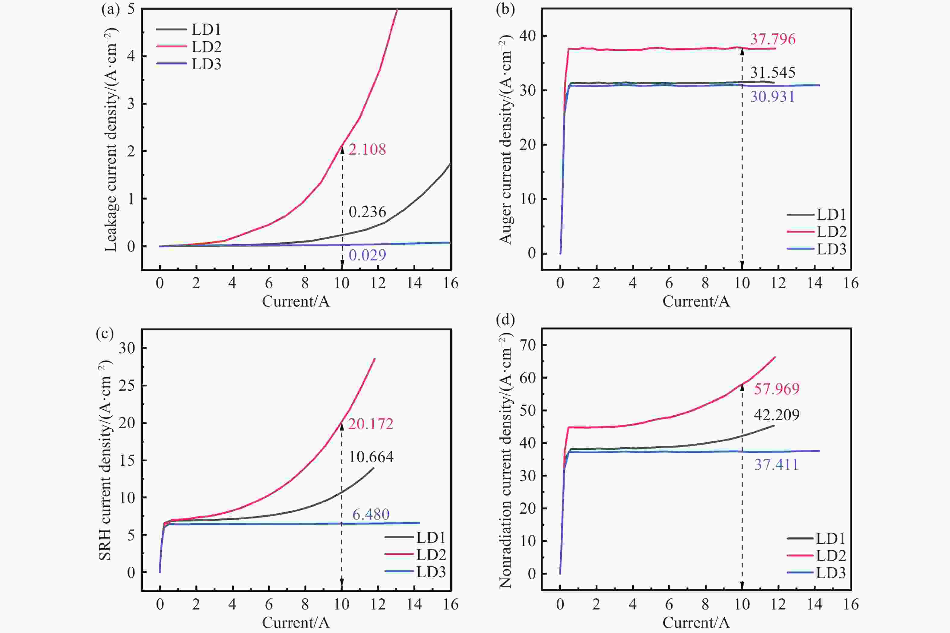
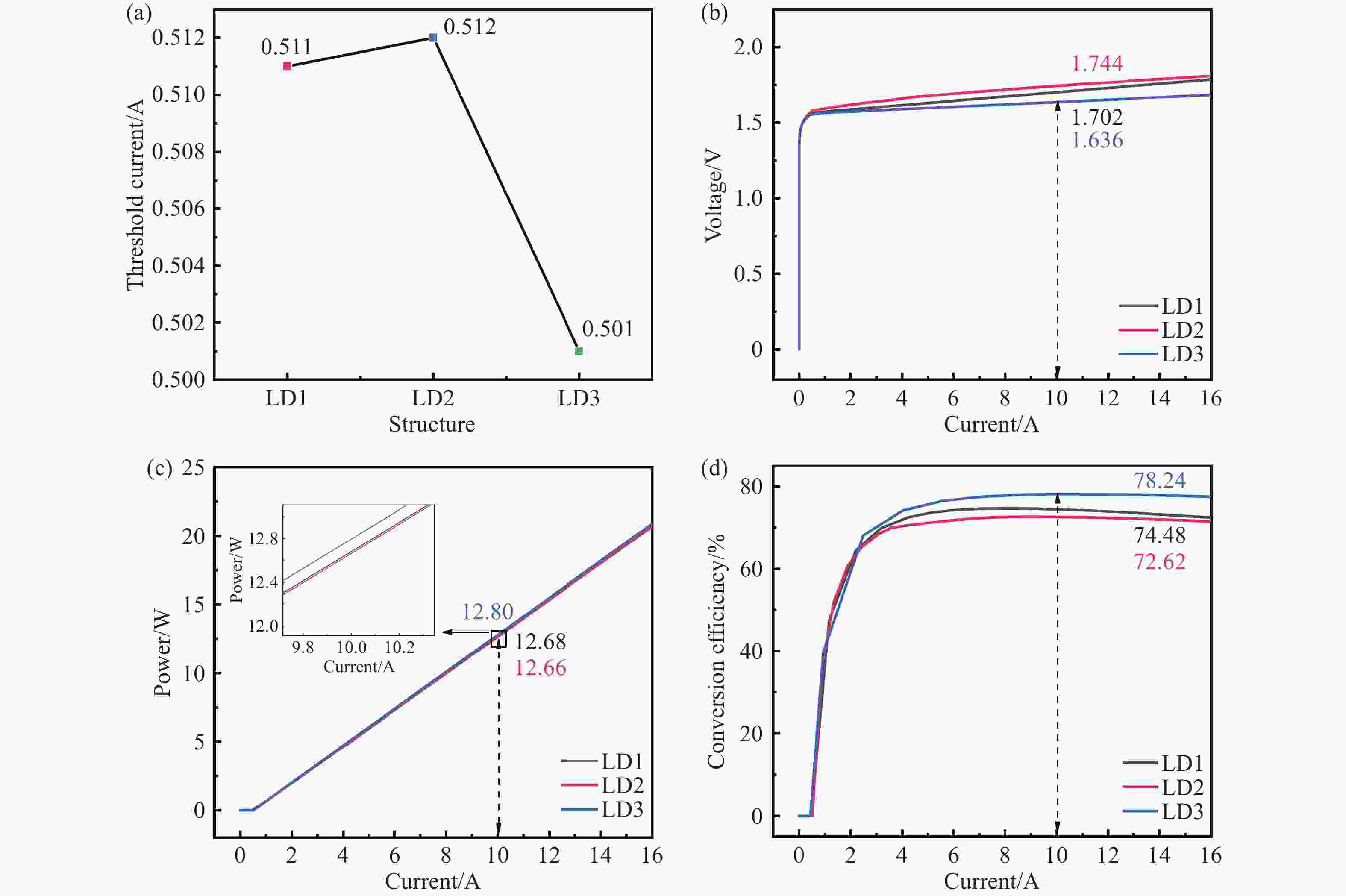
激光二极管由于载流子泄漏严重,在波导区域发生非辐射复合,进而降低了输出功率和电光转换效率。本文设计了一种新型外延结构,通过在有源区两侧势垒和波导层之间分别插入n-Ga0.55In0.45P和p-GaAs0.6P0.4材料,调控能带结构,增大了阻挡载流子泄漏的势垒高度,抑制了载流子泄漏。研究结果表明,相较于传统结构器件,泄漏电流密度降低了87.71%。在25 °C注入电流密度为5 A/cm2时,新型外延结构的非辐射复合电流密度降低至37.411 A/cm2,输出功率达12.80 W,电光转换效率达78.24%。此外,在5 °C~65 °C温度变化范围内,中心波长的温漂系数为0.206 nm/°C,阈值电流随温度变化的拟合直线的斜率为
0.00113 。本文所设计结构为制备高功率激光二级管提供了理论依据。-
关键词:
- 808-nm激光二极管 /
- Ga0.55In0.45P和GaAs0.6P0.4插入层 /
- InAlGaAs量子阱 /
- 载流子泄漏
Abstract:There is nonradiative recombination in waveguide region owing to severe carrier leakage, which in turn reduces output power and wall-plug efficiency. In this paper, we designed a novel epitaxial structure, which suppresses carrier leakage by inserting n-Ga0.55In0.45P and p-GaAs0.6P0.4 between barriers and waveguide layers, respectively, to modulate the energy band structure and to increase the height of barrier. The results show that the leakage current density reduces by 87.71%, compared to traditional structure. The nonradiative recombination current density of novel structure reduces to 37.411 A/cm2, and the output power reaches 12.80 W with wall-plug efficiency of 78.24% at an injection current density 5 A/cm2 at room temperature. In addition, the temperature drift coefficient of center wavelength is 0.206 nm/°C at the temperature range from 5 °C to 65 °C, and the slope of fitted straight line of threshold current with temperature variation is 0.00113. The novel epitaxial structure provides a theoretical basis for achieving high-power laser diode.
-
Table 1. Parameters of 808-nm LD’s epitaxial structures
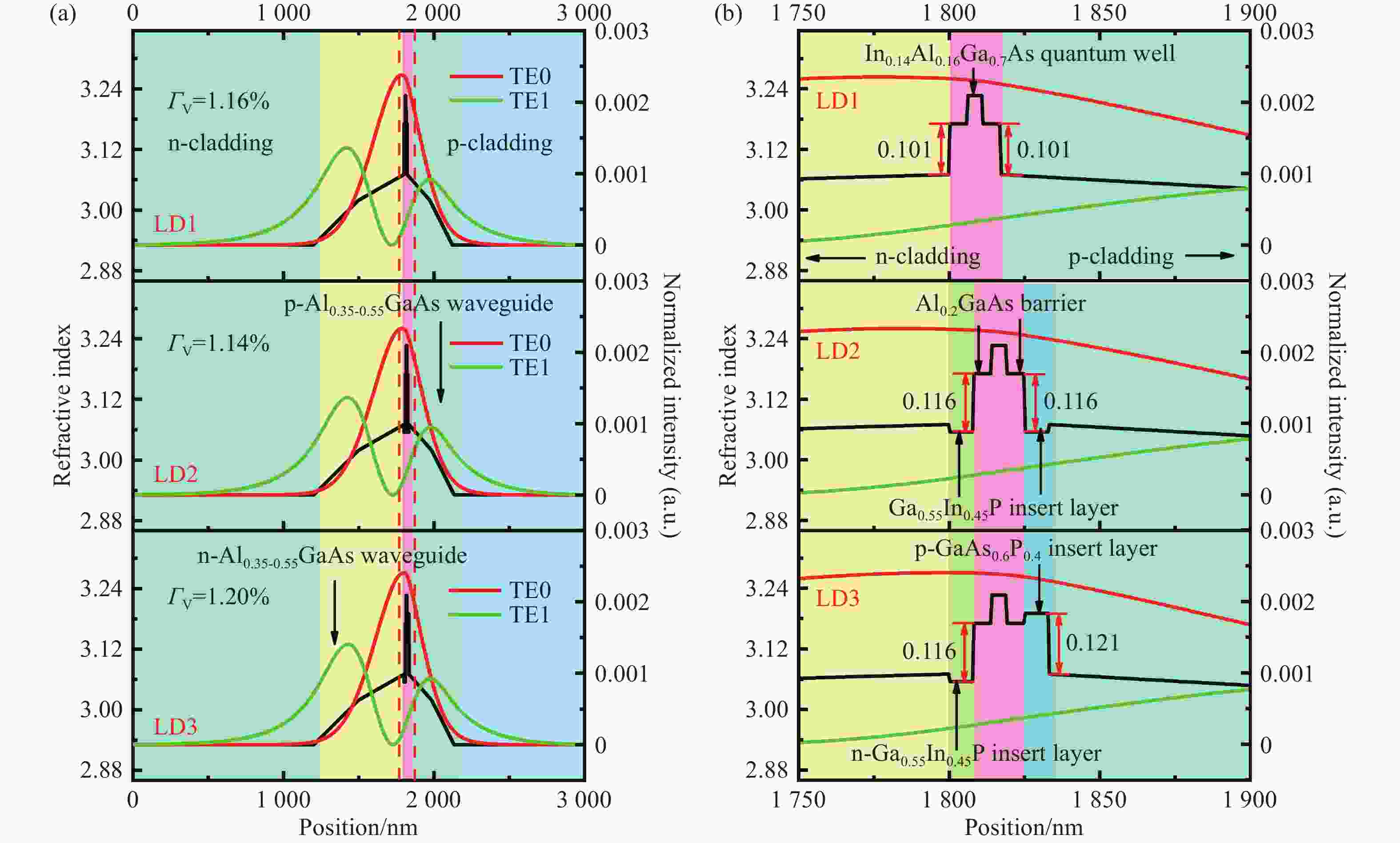
Structure layer Materials Thicknesses /nm Doping concentration /cm−3 p-Contact layer GaAs 350 1×10¹⁹ p-Cladding layer Al0.55Ga0.45As 1000 1×10¹⁹ p-Waveguide layer Al0.35-0.55Ga0.65-0.45As 300 1×10¹⁷~1×10¹⁸ p-Insertion layer Ga0.55In0.45P/GaAs0.6P0.4 8 1×10¹⁷ p-Barrier layer Al0.2Ga0.8As 6 0 Quantum well In0.14Al0.16Ga0.7As 5 0 n-Barrier layer Al0.2Ga0.8As 6 0 n-Insertion layer Ga0.55In0.45P 8 1×10¹⁷ n-Waveguide layer Al0.35-0.55Ga0.65-0.45As 600 1×10¹⁷~1×10¹⁸ n-Cladding layer Al0.55Ga0.45As 1200 1×10¹⁹ n-Substrate GaAs 2000 1×10¹⁹ -
[1] CRUMP P, ERBERT G, WENZEL H, et al. Efficient high-power laser diodes[J]. IEEE Journal of Selected Topics in Quantum Electronics, 2013, 19(4): 1501211. doi: 10.1109/JSTQE.2013.2239961 [2] KAUSHAL H, KADDOUM G. Applications of lasers for tactical military operations[J]. IEEE Access, 2017, 5: 20736-20753. doi: 10.1109/ACCESS.2017.2755678 [3] LI X Y, JIANG K, ZHU ZH, et al. High-brightness 808 nm semiconductor laser diode packaged by SiC heat sink[J]. Journal of Modern Optics, 2020, 67(11): 1017-1021. doi: 10.1080/09500340.2020.1810339 [4] REHIOUI O, BECHOU L, FILLARDET T, et al. Degradation analysis of individual emitters in 808nm QCW laser diode array for space applications[J]. Proceedings of SPIE, 2010, 7583: 758314. doi: 10.1117/12.840671 [5] WANG B G, TAN SH Y, ZHOU L, et al. High reliability 808nm laser diodes with output power over 19W under CW operation[J]. IEEE Photonics Technology Letters, 2022, 34(6): 349-352. doi: 10.1109/LPT.2022.3156913 [6] FREVERT C, CRUMP P, BUGGE F, et al. The impact of low Al-content waveguides on power and efficiency of 9xx nm diode lasers between 200 and 300 K[J]. Semiconductor Science and Technology, 2016, 31(2): 025003. doi: 10.1088/0268-1242/31/2/025003 [7] ZHANG B, WANG H ZH, WANG X, et al. Effect of GaAs insertion layer on the properties improvement of InGaAs/AlGaAs multiple quantum wells grown by metal-organic chemical vapor deposition[J]. Journal of Alloys and Compounds, 2021, 872: 159470. doi: 10.1016/j.jallcom.2021.159470 [8] CAO Y L, LIAN P, MA W Q, et al. Influence of GaAsP insertion layers on performance of InGaAsP/InGaP/AlGaAs quantum-well laser[J]. Chinese Physics Letters, 2006, 23(9): 2583-2586. doi: 10.1088/0256-307X/23/9/065 [9] LI X, ZHAO D G, JIANG D SH, et al. Suppression of electron leakage in 808 nm laser diodes with asymmetric waveguide layer[J]. Journal of Semiconductors, 2016, 37(1): 014007. doi: 10.1088/1674-4926/37/1/014007 [10] ASRYAN L V, ZUBOV F I, KRYZHANOVSKAYA N V, et al. Lasers with asymmetric barrier layers: a promising type of injection lasers[J]. Journal of Physics: Conference Series, 2016, 741: 012111. doi: 10.1088/1742-6596/741/1/012111 [11] ZUBOV F I, MURETOVA M E, ASRYAN L V, et al. Feasibility study for Al-free 808 nm lasers with asymmetric barriers suppressing waveguide recombination[J]. Journal of Applied Physics, 2018, 124(13): 133105. doi: 10.1063/1.5039442 [12] ZHANG X, DONG H L, JIA ZH G, et al. Effect of Ga1−xInxAs1−yPy Al-free asymmetric barrier on GaAs-based 808-nm laser diode[J]. Optics Letters, 2022, 47(5): 1153-1156. [13] YUAN Q H, JING H Q, ZHONG L, et al. High-power and high-reliability 9XX-nm laser diode[J]. Chinese Journal of Lasers, 2020, 47(4): 0401006. (in Chinese). doi: 10.3788/CJL202047.0401006 [14] ZHANG J, NING Y Q, ZENG Y G, et al. Design and analysis of high-temperature operating 795 nm VCSELs for chip-scale atomic clocks[J]. Laser Physics Letters, 2013, 10(4): 045802. doi: 10.1088/1612-2011/10/4/045802 [15] ZHANG Y, NING Y Q, ZHANG L S, et al. Design and comparison of GaAs, GaAsP and InGaAlAs quantum-well active regions for 808-nm VCSELs[J]. Optics Express, 2011, 19(13): 12569-12581. doi: 10.1364/OE.19.012569 [16] LAN Y, YANG G W, LIU Y X, et al. 808 nm broad-area laser diodes designed for high efficiency at high-temperature operation[J]. Semiconductor Science and Technology, 2021, 36(10): 105012. doi: 10.1088/1361-6641/ac2160 [17] SLIPCHENKO S O, VINOKUROV D A, PIKHTIN N A, et al. Ultralow internal optical loss in separate-confinement quantum-well laser heterostructures[J]. Semiconductors, 2004, 38(12): 1430-1439. doi: 10.1134/1.1836066 [18] LIU Y X, YANG G W, ZHAO Y M, et al. 48 W continuous-wave output from a high-efficiency single emitter laser diode at 915 nm[J]. IEEE Photonics Technology Letters, 2022, 34(22): 1218-1221. doi: 10.1109/LPT.2022.3207786 [19] MAN Y X, ZHONG L, MA X Y, et al. 975 nm semiconductor lasers with ultra-low internal optical loss[J]. Acta Optica Sinica, 2020, 40(19): 1914001. (in Chinese). doi: 10.3788/AOS202040.1914001 [20] AVRUTIN E A, RYVKIN B S, KOSTAMOVAARA J T. AlGaAs/GaAs asymmetric-waveguide, short cavity laser diode design with a bulk active layer near the p-cladding for high pulsed power emission[J]. IET Optoelectronics, 2021, 15(4): 194-199. doi: 10.1049/ote2.12033 [21] RYVKIN B S, AVRUTIN E A. Asymmetric, nonbroadened large optical cavity waveguide structures for high-power long-wavelength semiconductor lasers[J]. Journal of Applied Physics, 2005, 97(12): 123103. doi: 10.1063/1.1928309 [22] ZUBOV F I, MURETOVA M E, PAYUSOV A S, et al. Parasitic recombination in a laser with asymmetric barrier layers[J]. Semiconductors, 2020, 54(3): 366-373. doi: 10.1134/S1063782620030203 [23] ZHANG X L, DONG H L, ZHANG X, et al. Reduction of nonradiative recombination for high-power 808 nm laser diode adopting InGaAsP/InGaAsP/GaAsP active region[J]. Optics Communications, 2023, 537: 129461. doi: 10.1016/j.optcom.2023.129461 [24] KHALFIN V B, GULAKOV A B, KOCHNEV I V, et al. The influence of leakage on the characteristics of QW lasers[J]. AIP Conference Proceedings, 1991, 240(1): 49-57. [25] KAIFUCHI Y, YOSHIDA K, YAMAGATA Y, et al. Enhanced power conversion efficiency in 900-nm range single emitter broad stripe laser diodes maintaining high power operability[J]. Proceedings of SPIE, 2019, 10900: 109000F. [26] XU B SH, QU K, WANG ZH Y, et al. Investigation of photoelectric performance of laser diode by regulation of p-waveguide layer thickness[J]. Optik, 2020, 200: 163458. doi: 10.1016/j.ijleo.2019.163458 [27] WU SH H, LI T, WANG ZH F, et al. Study of temperature effects on the design of active region for 808 nm high-power semiconductor laser[J]. Crystals, 2023, 13(1): 85-99. doi: 10.3390/cryst13010085 [28] WENZEL H, ERBERT G, BUGGE F, et al. Optimization of GaAsP-QWs for high-power diode lasers at 800 nm[J]. Proceedings of SPIE, 2000, 3947: 32-38. doi: 10.1117/12.382104 -


 下载:
下载:
