


Mid-infrared plasmon regulation based on graphene nanoribbons
doi: 10.3788/CO.2019-0185
-
摘要: 石墨烯在中红外和太赫兹波段可以产生表面等离激元,并且通过合理设计还可以对其表面等离激元进行调控。基于此,本文设计了一种共振可调结构。通过在电介质基底上沉积不同宽度的单层石墨烯条带,引入纳米尺度上的不连续性,从而有效控制石墨烯与光的相互作用。使用时域有限差分法对该结构的光谱和电磁场分布进行了理论研究。结果表明:当所设计的结构与入射光耦合时,会出现多个共振增强的吸收峰;改变每个周期内石墨烯条带的数目、带宽和带间距,可以控制共振峰的个数、位置和强度;另外,施加不同的偏置电压可以改变石墨烯带的费米能级,从而实现共振峰位置和强度的动态调控;该结构可以在较宽光谱范围内调控石墨烯等离激元。本文研究为设计中红外波段基于石墨烯的传感、滤波、吸收等器件提供了理论基础。Abstract: Surface plasmon can be produced in graphene in the mid-infrared and terahertz waveband regimes, and the regulation for surface plasmon can be achieved by a reasonable design. On the basis of above, a resonant tunable structure was designed. By depositing single layers of graphene ribbons with different widths on a dielectric substrate, discontinuities in nanoscale were introduced, thereby effectively controlling the interaction of graphene with light. The spectral and electromagnetic field distributions of the structure were theoretically studied using the finite difference time domain method. The results showed that when the designed structure was coupled with the incident light, there would be multiple resonance enhanced absorption peaks. By changing the number, width and distance of the graphene ribbons in each period, the number, position, intensity of the resonance peak can be controlled. In addition, the Fermi energy level of graphene can be changed by applying different bias voltages, so the position and intensity of resonance peak can be adjusted dynamically. Therefore, with this structure graphene plasmon resonance can be regulated over a wide spectral range. This study provides a theoretical basis for the design of the graphene-based sensors, filters and absorbers in infrared regime.
-

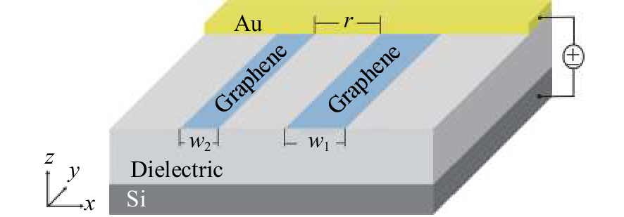
图 1 具有栅极控制的石墨烯纳米条带阵列一个周期的示意图。纳米带的宽度分别为
${w_1}$ ,${w_2}$ ,带间距离为rFigure 1. Schematic diagram of graphene nanoribbon array with grid control within one period. The widths of the nanoribbons are
${w_1}$ and${w_2}$ . The distance between the ribbons is$r$ 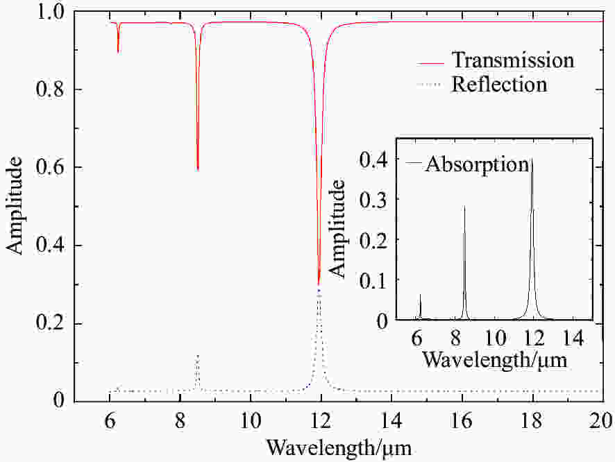
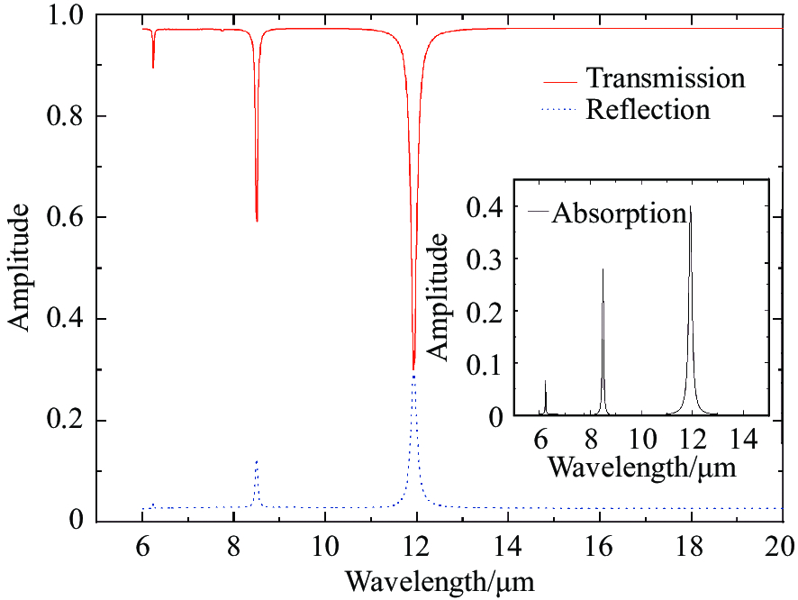
图 2 石墨烯纳米带结构的透射、反射、吸收(插图)光谱。纳米带宽度w1 = 200 nm,w2 = 100 nm,带间距离r = 100 nm
Figure 2. Transmission, reflection and absorption (illustration) spectra of graphene nanoribbon structure. The widths of the nanoribbons are w1 = 200 nm and w2 = 100 nm, respectively. The distance between the nanoribbons is r = 100 nm
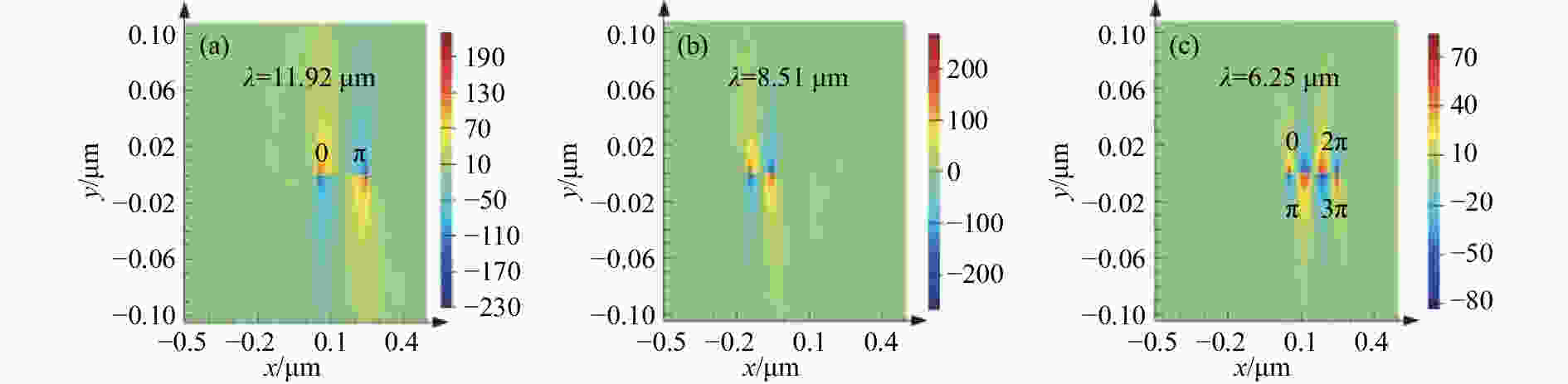
图 3 不同共振波长下,z方向电场强度Ez的分布图。入射光波长分别为11.92,8.51,6.25 μm
Figure 3. Distributions of the electric field intensity Ez in z direction at different resonance wavelengths. The wavelengths of incident light are 11.92, 8.51 and 6.25 μm respectively
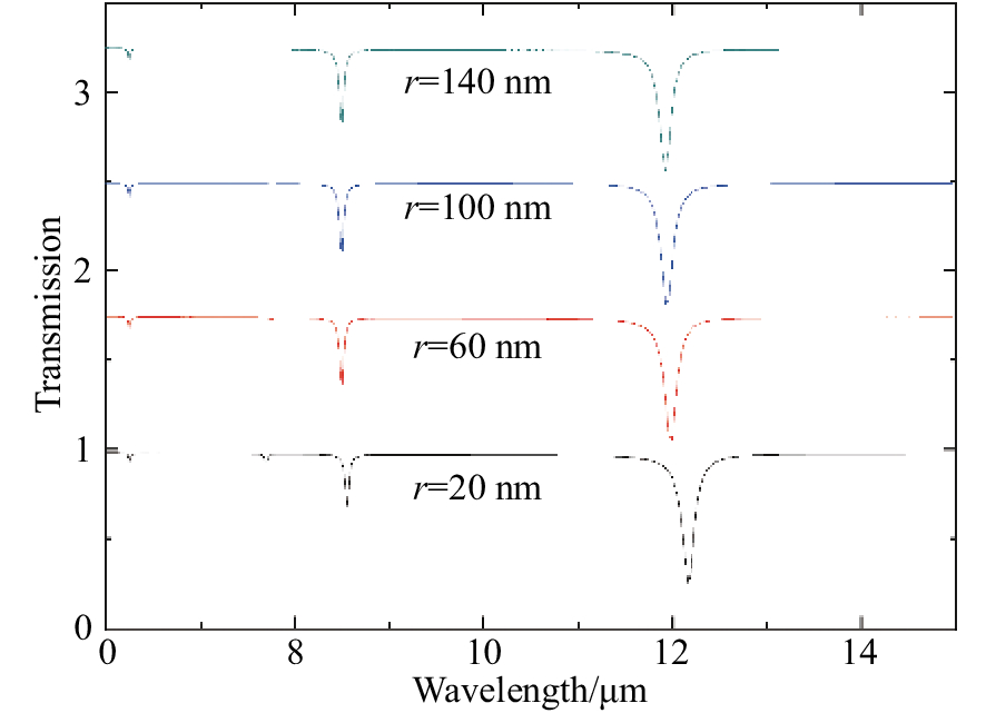
图 4 石墨烯纳米带间距变化时,结构的透射光谱
Figure 4. Transmission spectra of the structure when the distance between graphene nanoribbons changes
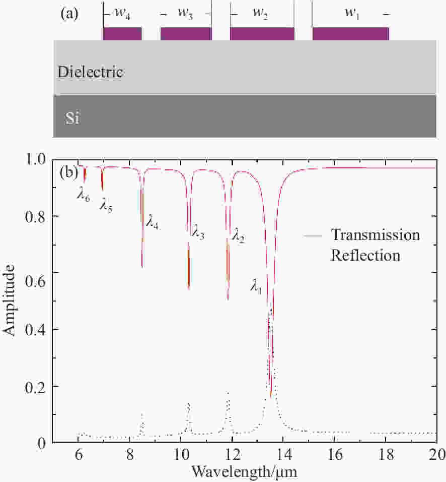
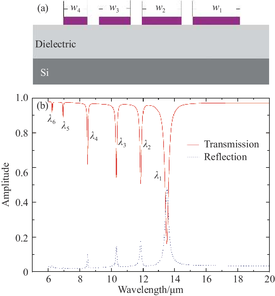
图 5 (a)为结构侧视图。一个周期内有4条石墨烯纳米带。条带宽度分别为250 nm,200 nm,150 nm,100 nm。(b)为该结构的透射谱、反射谱
Figure 5. (a) Side view of the structure. There are four graphene nanoribbons in one period. The widths of the nanoribbons are 250 nm, 200 nm, 150 nm and 100 nm respectively. (b) Transmission and reflection spectra of the structure

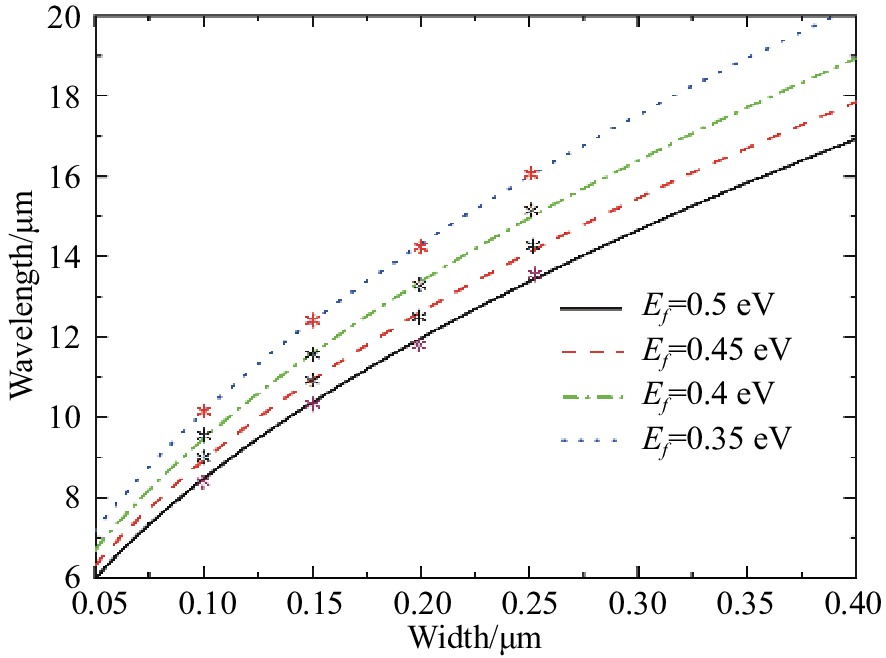
图 6 不同费米能级下,共振波长与石墨烯带宽度的关系
Figure 6. Relationship between resonant wavelength and graphene ribbon width at different fermi levels
-
[1] YU N F, WANG Q J, KATS M A, et al. Designer spoof surface plasmon structures collimate terahertz laser beams[J]. Nature Materials, 2010, 9(9): 730-735. doi: 10.1038/nmat2822 [2] GEIM A K, NOVOSELOV K S. The rise of graphene[J]. Nature Materials, 2007, 6(3): 183-191. doi: 10.1038/nmat1849 [3] GRIGORENKO A N, POLINI M, NOVOSELOV K S. Graphene plasmonics[J]. Nature Photonics, 2012, 6(11): 749-758. doi: 10.1038/nphoton.2012.262 [4] LIU P W, JIN ZH, KATSUKIS G, et al. Layered and scrolled nanocomposites with aligned semi-infinite graphene inclusions at the platelet limit[J]. Science, 2016, 353(6297): 364-367. doi: 10.1126/science.aaf4362 [5] HAN S J, GARCIA A V, OIDA S, et al. Graphene radio frequency receiver integrated circuit[J]. Nature Communications, 2014, 5: 3086. doi: 10.1038/ncomms4086 [6] REN L, ZHANG Q, YAO J, et al. Terahertz and infrared spectroscopy of gated large-area graphene[J]. Nano Letters, 2012, 12(7): 3711-3715. doi: 10.1021/nl301496r [7] FEI Z, RODIN A S, ANDREEV G O, et al. Gate-tuning of graphene plasmons revealed by infrared nano-imaging[J]. Nature, 2012, 487(7405): 82-85. doi: 10.1038/nature11253 [8] MIAO X CH, TONGAY S, PETTERSON M K, et al. High efficiency graphene solar cells by chemical doping[J]. Nano Letters, 2012, 12(6): 2745-2750. doi: 10.1021/nl204414u [9] CAI X H, SUSHKOV A B, JADIDI M M, et al. Plasmon-enhanced terahertz photodetection in graphene[J]. Nano Letters, 2015, 15(7): 4295-4302. doi: 10.1021/acs.nanolett.5b00137 [10] GAO W L, SHU J, REICHEL K, et al. High-contrast terahertz wave modulation by gated graphene enhanced by extraordinary transmission through ring apertures[J]. Nano Letters, 2014, 14(3): 1242-1248. doi: 10.1021/nl4041274 [11] TAVAKOL M R, RAHMANI B, KHAVASI A. Tunable polarization converter based on one-dimensional graphene metasurfaces[J]. Journal of the Optical Society of America B, 2018, 35(10): 2574-2581. doi: 10.1364/JOSAB.35.002574 [12] TAVAKOL M R, SABA A, JAFARGHOLI A, et al. Terahertz spectrum splitting by a graphene-covered array of rectangular grooves[J]. Optics Letters, 2017, 42(23): 4808-4811. doi: 10.1364/OL.42.004808 [13] KIM S, JANG M S, BRAR V W, et al. Electronically tunable extraordinary optical transmission in graphene plasmonic ribbons coupled to subwavelength metallic slit arrays[J]. Nature Communications, 2016, 7: 12323. doi: 10.1038/ncomms12323 [14] FARHAT M, GUENNEAU S, BAĞCI H. Exciting graphene surface plasmon polaritons through light and sound interplay[J]. Physical Review Letters, 2013, 111(23): 237404. doi: 10.1103/PhysRevLett.111.237404 [15] GARCIA-POMAR J L, NIKITIN A Y, MARTIN-MORENO L. Scattering of graphene plasmons by defects in the graphene sheet[J]. ACS Nano, 2013, 7(6): 4988-4994. doi: 10.1021/nn400342v [16] YAN H G, LI X S, CHANDRA B, et al. Tunable infrared plasmonic devices using graphene/insulator stacks[J]. Nature Nanotechnology, 2012, 7(5): 330-334. doi: 10.1038/nnano.2012.59 [17] JIN ZH, SUN W, KE Y G, et al. Metallized DNA nanolithography for encoding and transferring spatial information for graphene patterning[J]. Nature Communications, 2013, 4: 1663. doi: 10.1038/ncomms2690 [18] RODRIGO D, TITTL A, LIMAJ O, et al. Double-layer graphene for enhanced tunable infrared plasmonics[J]. Light:Science &Applications, 2017, 6(6): e16277. [19] HUANG L, HU G H, DENG C Y, et al. Realization of mid-infrared broadband absorption in monolayer graphene based on strong coupling between graphene nanoribbons and metal tapered grooves[J]. Optics Express, 2018, 26(22): 29192-29202. doi: 10.1364/OE.26.029192 [20] ZHAO B, ZHANG ZH M. Strong plasmonic coupling between graphene ribbon array and metal gratings[J]. ACS Photonics, 2015, 2(11): 1611-1618. doi: 10.1021/acsphotonics.5b00410 [21] LI K, FITZGERALD J M, XIAO X F, et al. Graphene plasmon cavities made with silicon carbide[J]. ACS Omega, 2017, 2(7): 3640-3646. doi: 10.1021/acsomega.7b00726 [22] FALKOVSKY L A. Optical properties of graphene[J]. Journal of Physics:Conference Series, 2008, 129: 012004. doi: 10.1088/1742-6596/129/1/012004 [23] MAK K F, SFEIR M Y, WU Y, et al. Measurement of the optical conductivity of graphene[J]. Physical Review Letters, 2008, 101(19): 196405. doi: 10.1103/PhysRevLett.101.196405 [24] DU L P, TANG D Y, YUAN X C. Edge-reflection phase directed plasmonic resonances on graphene nano-structures[J]. Optics Express, 2014, 22(19): 22689-22698. doi: 10.1364/OE.22.022689 [25] CHEN J N, NESTEROV M L, NIKITIN A Y, et al. Strong plasmon reflection at nanometer-size gaps in monolayer graphene on SiC[J]. Nano Letters, 2013, 13(12): 6210-6215. doi: 10.1021/nl403622t [26] LI Z Q, HENRIKSEN E A, JIANG Z, et al. Dirac charge dynamics in graphene by infrared spectroscopy[J]. Nature Physics, 2008, 4(7): 532-535. doi: 10.1038/nphys989 [27] WANG F, ZHANG Y B, TIAN CH SH, et al. Gate-variable optical transitions in graphene[J]. Science, 2008, 320(5873): 206-209. doi: 10.1126/science.1152793 -


 下载:
下载:


计量
- 文章访问数: 2371
- HTML全文浏览量: 948
- PDF下载量: 114
- 被引次数: 0
