


Design and research of Ge/Si avalanche photodiode with a specific lateral carrier collection structure
-
摘要: 为了实现高效的微光探测以及满足量子通信的需求,需要研发制备具有高增益、低噪声和高带宽的高性能红外探测器,基于硅衬底材料的锗硅雪崩探测器(Avalanche Photodiode, APD)被认为是有希望实现近红外通信波段高效弱光探测的探测器件。本工作设计研究了一种横向收集结构的锗硅APD,并对其结构参数对电场分布的影响进行了仿真模拟。发现该结构中硅倍增层的掺杂浓度、尺寸等对器件电场分布具有很重要的影响,并且利用能带理论对其进行了解释说明。倍增层掺杂浓度提高后,增强的结效应导致该器件中出现了有趣的双结结构,横向的n+-n-结与纵向的p+-i-p--n-结共同作用于电场分布,并且实现了纵向雪崩与横向载流子收集。在-30 dBm 1 310 nm光源正入射下,新设计的横向吸收结构APD经过优化带宽可以达到20 GHz;线性响应度0.7 A/W;由于采用了键合方法,其暗电流可以下降至10-12 A。基本满足近红外通信波段弱光探测的高速、低暗电流、探测能力强等要求。Abstract: In order to achieve infrared photodetectors with high gain, low noise, and high 3 dB-bandwidth(3 dB-BW) for low-loss and high-efficiency fiber communication, many researchers have paid attention to the Ge/Si avalanche photodiode(APD) which is regarded as a potential photoelectric device for the detection of infrared light. In this paper, we propose and theoretically study a potential structure of a Ge/Si APD with a specific lateral carrier collection structure. The influence on the electric field distribution of the doping concentration of the top Si layer, the size of the gap between heavily-doped n-Si and the Ge/Si mesa, and the thickness of the top Si layer thickness have been considered. It was found that the doping concentration of Si multiplication significantly affects the junction effect of the vertical p+-i-p--n- junction and lateral n+-n- junction, which in turn affects the distribution of the electric field. Furthermore, the reason for the high 3 dB-BW is also clarified by studying the carrier transportation. This feature is explained by the high carrier velocity in the direction of carrier collection induced by the fringing electric field formed by the lateral n+-n- and vertical p+-i-p--n- junction structure. It was found that the migration path of carriers in our lateral collection APD is along the edge of the Ge mesa and turns to the lateral direction in the Si layer. This is very different from the vertical migration path in a traditional SACM Ge/Si APD. We researched and found that an extremely low dark current can be obtained using an oxide-free Ge/Si direct wafer bond. A high 3 dB-bandwidth of~20 GHz was achieved under an optical input power of -30 dBm at 1 310 nm. Such a high 3 dB-bandwidth is demonstrated using the specific lateral carrier collection structure of this APD.
-
Key words:
- semiconductor detectors /
- avalanche photodiodes /
- Ge/Si /
- electric field control
-

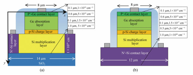
图 1 (a) 横向吸收结构与(b)传统纵向SACM结构Ge/Si APD的结构示意图
Figure 1. Schematic diagrams of the (a)lateral-collection Ge/Si APD and (b)traditional vertical SACM Ge/Si APD

图 2 30 V反向偏压下Ge/Si APD的电场分布图(线性坐标)。(a)最早设计的APD结构,其具有0.5 μm的Si层厚度,掺杂浓度为5×1015 cm-3。(b)在高掺Si层和台面间添加了1 μm Gap后的器件结构。(c)对应的I-V曲线
Figure 2. Electric fields of Ge/Si APDs at 30 V reverse bias in linear coordinates. (a)The original APD with 0.5 μm top Si layer(doping concentration of 5×1015 cm-3), (b)the optimized APD with a gap of 1 μm between the mesa and n+-Si layer, (c)I-V curves

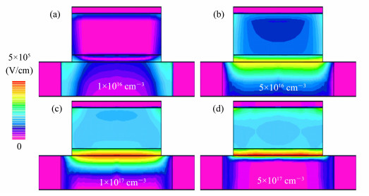
图 3 30 V反向偏压下不同Si倍增层掺杂浓度的Ge/Si APD的电场分布图(线性坐标)。(a)1×1016 cm-3; (b)5×1016 cm-3; (c)1×1017 cm-3; (d)5×1017 cm-3
Figure 3. Electric fields (linear coordinate) of Ge/Si APDs with the doping concentrations of (a)1×1016 cm-3, (b)5×1016 cm-3, (c)1×1017 cm-3, and (d)5×1017 cm-3 at 30 V reverse bias

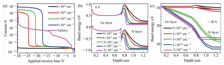
图 4 (a) I-V曲线; (b)0 V偏压下的器件能带模拟图; (c)30 V偏压下的器件能带模拟图
Figure 4. (a)I-V curves, (b)energy band diagrams of devices at 0 V bias, and (c)at 30 V bias with different doping concentration of top Si layer

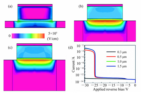
图 5 不同厚度Si层电场分布示意图及其I-V曲线。(a)300 nm;(b)1 μm;(c)1.5 μm(d)I-V曲线
Figure 5. Electric fields(linear coordinate) of Ge/Si APDs with (a)300 nm, (b)1 μm, and (c)1.5 μm thick top Si layer and (d)corresponding I-V curves

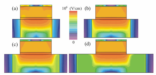
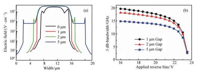
图 6 不同宽度gap区电场分布示意图(对数坐标)。(a)0 μm;(b)1 μm;(c)2 μm;(d)5 μm
Figure 6. Electric fields(logarithmic coordinates) of Ge/Si APDs with (a)0 μm, (b)1 μm, (c)2 μm, and (d)5 μm wide gap region

图 7 不同宽度gap区的(a)横向电场分布和(b)对应的3 dB带宽
Figure 7. Lateral electric fields(a) and the related 3 dB-BW(b) of the APDs with different width of gaps

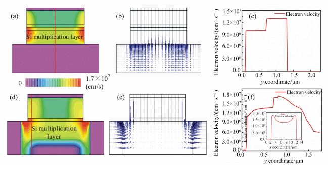
图 8 纵向SACM结构APD的(a)电子速率;(b)电流方向(和电子输运方向相反)和(c)纵向电子速率分布;本文设计的横向吸收结构APD的(d)电子速率;(e)电流方向(和电子输运方向相反)和(f)纵向电子速率分布,插图中是横向速率分布
Figure 8. (a)-(c) The electron velocity(linear coordinates), direction of current flow(contrary to electrons transport) and vertical electron velocity curve in edge of SACM APD; (d)-(f)the electron velocity, direction of current flow and vertical electron velocity curve of proposed APD. Inset shows the lateral electron velocity

图 9 不同Ge吸收层厚度(0.5 μm,0.6 μm,0.7 μm)模拟得到的(a)I-V曲线、增益和(b)3dB带宽
Figure 9. (a)I-V curves, gain and (b)3 dB-BW of devices with different Ge absorption layer thicknesses(0.5 μm, 0.6 μm, 0.7 μm) under an optical input power of -30 dBm at 1 310 nm
表 1 不同结构Ge/Si APD的性能对比
Table 1. Performance comparison obtained by Ge/Si APD with different structures
 下载: 导出CSV
-
[1] GUO Q S, POSPISCHIL A, BHUIYAN M, et al.. Black phosphorus mid-infrared photodetectors with high gain[J]. Nano Letters, 2016, 16(7):4648-4655. doi: 10.1021/acs.nanolett.6b01977 [2] MIAO J SH, HU W D, GUO N, et al.. High-responsivity graphene/InAs nanowire heterojunction near-infrared photodetectors with distinct photocurrent on/off ratios[J]. Small, 2015, 11(8):936-942. doi: 10.1002/smll.201402312 [3] 逯丹凤, 刘瑞鹏, 祁志美.基于多层膜敏感圆片的光学式有机磷快速检测方法[J].分析化学, 2011, 39(6):934-938. http://d.old.wanfangdata.com.cn/Periodical/fxhx201106031LU D F, LIU R P, QI ZH M. An optical method for rapid detection of organophosphates based on multilayer-disc sensing element[J]. Chinese Journal of Analytical Chemistry, 2011, 39(6):934-938.(in Chinese) http://d.old.wanfangdata.com.cn/Periodical/fxhx201106031 [4] 张维冰, 王智聪, 张凌怡.超高效液相色谱-光电二极管阵列检测-串联四级杆质谱法测定红洋葱中黄酮醇及其糖苷类化合物[J].分析化学, 2014, 42(3):415-422. http://d.old.wanfangdata.com.cn/Periodical/fxhx201403018ZHANG W B, WANG ZH C, ZHANG L Y. Determination of flavonols and flavonol glycosides in red onion by ultra high performance liquid chromatography-photodiode array detection-tandem quadrupole mass spectrometry[J]. Chinese Journal of Analytical Chemistry, 2014, 42(3):415-422.(in Chinese) http://d.old.wanfangdata.com.cn/Periodical/fxhx201403018 [5] MARTINEZ N J D, GEHL M, DEROSE C T, et al.. Single photon detection in a waveguide-coupled Ge-on-Si lateral avalanche photodiode[J]. Optics Express, 2017, 25(14):16130-16139. doi: 10.1364/OE.25.016130 [6] WOODSON M E, REN M, MADDOX S J, et al.. Low-noise AlInAsSb avalanche photodiode[J]. Applied Physics Letters, 2016, 108(8):081102. doi: 10.1063/1.4942372 [7] WEN J, WANG W J, CHEN X R, et al.. Origin of large dark current increase in InGaAs/InP avalanche photodiode[J]. Journal of Applied Physics, 2018, 123(16):161530. doi: 10.1063/1.4999646 [8] TU J J, ZHAO Y L, WEN K, et al.. The determination of unity gain for InGaAs/InP avalanche photodiodes with excess noise measurements[J]. IEEE Photonics Technology Letters, 2017, 29(8):671-674. doi: 10.1109/LPT.2017.2676028 [9] HE D Y, WANG SH, CHEN W, et al.. Sine-wave gating InGaAs/InP single photon detector with ultralow after pulse[J]. Applied Physics Letters, 2017, 110(11):111104. doi: 10.1063/1.4978599 [10] MA Y J, ZHANG Y G, GU Y, et al.. Impact of etching on the surface leakage generation in mesa-type InGaAs/InAlAs avalanche photodetectors[J]. Optics Express, 2016, 24(7):7823-7834. doi: 10.1364/OE.24.007823 [11] YIN D D, YANG X H, HE T T, et al.. InGaAs/InAlAs avalanche photodetectors integrated on silicon-on-insulator waveguide circuits[J]. Journal of Optical Technology, 2017, 84(5):350-354. doi: 10.1364/JOT.84.000350 [12] CHEN H T, VERBIST J, VERHEYEN P, et al.. High sensitivity 10 Gb/s Si photonic receiver based on a low-voltage waveguide-coupled Ge avalanche photodetector[J]. Optics Express, 2015, 23(2):815-822. doi: 10.1364/OE.23.000815 [13] VIROT L, CROZAT P, FÉDÉLI J M, et al..Germanium avalanche receiver for low power interconnects[J]. Nature Communications, 2014, 5:4957. doi: 10.1038/ncomms5957 [14] MICHELJ, LIU J F, KIMERLING L C. High-performance Ge-on-Si photodetectors[J]. Nature Photonics, 2010, 4(8):527-534. doi: 10.1038/nphoton.2010.157 [15] SAMAVEDAM S B, CURRIE M T, LANGDO T A, et al.. High-quality germanium photodiodes integrated on silicon substrates using optimized relaxed graded buffers[J]. Applied Physics Letters, 1998, 73(15):2125-2127. doi: 10.1063/1.122399 [16] KE SH Y, YE Y J, LIN SH M, et al.. Low-temperature oxide-free silicon and germanium wafer bonding based on a sputtered amorphous Ge[J]. Applied Physics Letters, 2018, 112(4):041601. doi: 10.1063/1.4996800 [17] KE SH Y, YE Y J, WU J Y, et al..Interface characteristics and electrical transport of Ge/Si heterojunction fabricated by low-temperature wafer bonding[J]. Journal of Physics D:Applied Physics, 2018, 51(26):265306. doi: 10.1088/1361-6463/aac7b0 [18] KE SH Y, LIN SH M, YE Y J, et al..Bubble evolution mechanism and stress-induced crystallization in low-temperature silicon wafer bonding based on a thin intermediate amorphous Gelayer[J]. Journal of Physics D:Applied Physics, 2017, 50(40):405305. doi: 10.1088/1361-6463/aa81ee [19] DUAN N, LIOW T Y, LIM E J, et al.. 310 GHz gain-bandwidth product Ge/Si avalanche photodetector for 1550 nm light detection[J]. Optics Express, 2012, 20(10):11031-11036. doi: 10.1364/OE.20.011031 [20] ZAOUI W S, CHEN H W, BOWERS J E, et al..Frequency response and bandwidth enhancement in Ge/Si avalanche photodiodes with over 840 GHz gain-bandwidth-product[J]. Optics Express, 2009, 17(15):12641-12649. doi: 10.1364/OE.17.012641 [21] KANG Y M, LIU H D, MORSE M, et al..Monolithic germanium/silicon avalanche photodiodes with 340 GHz gain-bandwidth product[J]. Nature Photonics, 2009, 3(1):59-63. doi: 10.1038/nphoton.2008.247 [22] SELBERHERR S. Analysis and Simulation of Semiconductor Devices[M]. Vienna:Springer, 1984. [23] HUANG SH H, LI CH, ZHOU ZH W, et al.. Depth-dependent etch pit density in Ge epilayer on Si substrate with a self-patterned Ge coalescence island template[J]. Thin Solid Films, 2012, 520(6):2307-2310. doi: 10.1016/j.tsf.2011.09.023 [24] ZHOU ZH W, HE J K, WANG R CH, et al.. Normal incidence p-i-n Geheterojunction photodiodes on Si substrate grown by ultrahigh vacuum chemical vapor deposition[J]. Optics Communications, 2010, 283(18):3404-3407. doi: 10.1016/j.optcom.2010.04.098 -

 下载:
下载:


计量
- 文章访问数: 3390
- HTML全文浏览量: 1115
- PDF下载量: 1156
- 被引次数: 0
