Fabrication and photoelectric properties of organic-inorganic broad-spectrum photodetectors based on Se microwire/perovskite heterojunction
-
摘要: 针对目前高效、稳定的p型掺杂一直较难实现的问题,本文采用化学气相沉积方法制备出了高结晶质量的p型半导体材料Se微米线。同时,还制备出了基于单根Se微米线的光电探测器,其在紫外和可见光波段有较宽的响应范围,响应截止边为675 nm。该器件在5 V偏压下的峰值响应度可达2.8 mA/W(600 nm)。在此基础上,利用p型Se微米线与钙钛矿材料CH3NH3PbCl3制备了p-n结型器件,与单根Se微米线光电探测器相比,响应时间和响应度都有明显提升,尤其是异质结的响应度比纯Se微米线提高了850%。这一研究结果说明本文制备的有机无机复合结构p-n结非常有望应用到高性能光电探测器中。
-
关键词:
- 光电探测器 /
- p型半导体 /
- 钙钛矿 /
- CH3NH3PbCl3
Abstract: Efficient and stable p-type doping is difficult to achieve. To solve this problem, high-quality p-type Se microwires were fabricated using chemical vapor deposition. A photodetector based on a single Se microtube shows broadband photoresponses with a peak responsivity of 2.8 mA/W at 600 nm under 5 V bias. The cutoff wavelength is estimated to be 675 nm. A p-n heterojunction photodetector using a p-type Se microwire and n-type CH3NH3PbCl3 was also fabricated. Compared to the single Se microtube, the p-n heterojunction photodetector shows obvious reduction in response time and 850% improvement in responsivity. The experimental results indicate that p-n junctions have promising applications in high-performance photodetectors.-
Key words:
- photodetector /
- p-type semiconductor /
- perovskite /
- CH3NH3PbCl3
-
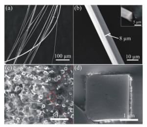
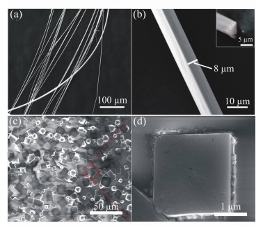
图 1 Se微米线的扫描电镜照片(a)低放大倍率; (b)单根Se微米线的放大图片。插图为微米线的断面图。(c)(d)分散在石英衬底上为不同倍率的MAPbCl3扫描电镜照片
Figure 1. SEM images of as-grown Se microwires on Si substrate. (a)Low magnification SEM image. (b)High magnification SEM image. The inset is the cross section of Se MW. (c), (d)The SEM images of as-grown MAPbCl3 on quartz substrate
-
[1] CHEN H Y, LIU H, ZHANG ZH M, et al.. Nanostructured photodetectors:from ultraviolet to terahertz[J]. Advanced Materials, 2016, 28(3):403-433. doi: 10.1002/adma.201503534 [2] ZHANG D, ZHENG W, LIN R C, et al.. High quality β-Ga2O3 film grown with N2O for high sensitivity solar-blind-ultraviolet photodetector with fast response speed[J]. Journal of Alloys and Compounds, 2018, 735:150-154. doi: 10.1016/j.jallcom.2017.11.037 [3] OH S, KIM C K, KIM J. High responsivity β-Ga2O3 metal-semiconductor-metal solar-blind photodetectors with ultraviolet transparent graphene electrodes[J]. ACS Photonics, 2018, 5(3):1123-1128. doi: 10.1021/acsphotonics.7b01486 [4] LI D B, JIANG K, SUN X J, et al.. Algan photonics:recent advances in materials and ultraviolet devices[J]. Advances in Optics and Photonics, 2018, 10(1):43-110. doi: 10.1364/AOP.10.000043 [5] XU ZH X, ZHANG Y L, WANG ZH N. ZnO-based photodetector:from photon detector to pyro-phototronic effect enhanced detector[J]. Journal of Physics D:Applied Physics, 2019, 52(22):223001. doi: 10.1088/1361-6463/ab0728 [6] 孙华山, 刘可为, 陈洪宇, 等.Au电极厚度对MgZnO紫外探测器性能的影响[J].发光学报, 2015, 36(2):200-205. http://www.wanfangdata.com.cn/details/detail.do?_type=perio&id=fgxb201502012SUN H SH, LIU K W, CHEN H Y, et al.. Effect of Au electrode thickness on the performance of MgZnO UV detector[J]. Chinese Journal of Luminescence, 2015, 36(2):200-205.(in Chinese) http://www.wanfangdata.com.cn/details/detail.do?_type=perio&id=fgxb201502012 [7] 薛金玲, 马剑钢.化学气相沉积法制备β-Ga2O3纳米结构及其缺陷发光性质研究[J].发光学报, 2017, 38(10):1273-1279. http://www.wanfangdata.com.cn/details/detail.do?_type=perio&id=fgxb201710002XUE J L, MA J G. Defects luminescence behavior of β-Ga2O3 nanostructures synthesized by chemical vapor deposition[J]. Chinese Journal of Luminescence, 2017, 38(10):1273-1279.(in Chinese) http://www.wanfangdata.com.cn/details/detail.do?_type=perio&id=fgxb201710002 [8] QI J, QIAO W Q, ZHOU X K, et al.. High-detectivity all-polymer photodetectors with spectral response from 300 to 1100 nm[J]. Macromolecular Chemistry and Physics, 2016, 217(15):1683-1689. doi: 10.1002/macp.201600061 [9] LUO L B, YANG X B, LIANG F X, et al.. Transparent and flexible selenium nanobelt-based visible light photodetector[J]. CrystEngComm, 2012, 14(6):1942-1947. doi: 10.1039/c2ce06420k [10] QIU X D, WANG Z J, HOU X T, et al.. Visible-blind short-wavelength infrared photodetector with high responsivity based on hyperdoped silicon[J]. Photonics Research, 2019, 7(3):351-358. doi: 10.1364/PRJ.7.000351 [11] YU P P, HU K, CHEN H Y, et al.. Novel p-p heterojunctions self-powered broadband photodetectors with ultrafast speed and high responsivity[J]. Advanced Functional Materials, 2017, 27(38):1703166. doi: 10.1002/adfm.201703166 [12] GONG F, FANG H H, WANG P, et al.. Visible to near-infrared photodetectors based on MoS2 vertical schottky junctions[J]. Nanotechnology, 2017, 28(48):484002. doi: 10.1088/1361-6528/aa9172 [13] WANG L, JIE J SH, SHAO ZH B, et al.. MoS2/Si heterojunction with vertically standing layered structure for ultrafast, high-detectivity, self-driven visible-near infrared photodetectors[J]. Advanced Functional Materials, 2015, 25(19):2910-2919. doi: 10.1002/adfm.201500216 [14] ROGALSKI A, ANTOSZEWSKI J, FARAONE L. Third-generation infrared photodetector arrays[J]. Journal of Applied Physics, 2009, 105(9):091101. doi: 10.1063/1.3099572 [15] MELEDIN D V, MARRONE D P, TONG C Y E, et al.. A 1-Thz superconducting hot-electron-bolometer receiver for astronomical observations[J]. IEEE Transactions on Microwave Theory and Techniques, 2004, 52(10):2338-2343. doi: 10.1109/TMTT.2004.835979 [16] TONG C Y E, MELEDIN D V, MARRONE D P, et al.. Near field vector beam measurements at 1 THz[J]. IEEE Microwave and Wireless Components Letters, 2003, 13(6):235-237. doi: 10.1109/LMWC.2003.814602 [17] MITTLEMAN D M. Twenty years of terahertz imaging[J]. Optics Express, 2018, 26(8):9417-9431. doi: 10.1364/OE.26.009417 [18] CHEN H Y, LIU K W, HU L F, et al.. New concept ultraviolet photodetectors[J]. Mater Today, 2015, 18(9):493-502. doi: 10.1016/j.mattod.2015.06.001 [19] SZE S M. Semiconductor Devices:Physics and Technology[M]. 2nd ed. New York:John Wiley & Sons, 2008. [20] ZHAO B, WANG F, CHEN H Y, et al.. An ultrahigh responsivity(9.7 mA W-1) self-powered solar-blind photodetector based on individual ZnO-Ga2O3 heterostructures[J]. Advanced Functional Materials, 2017, 27(17):1700264. doi: 10.1002/adfm.201700264 [21] HAJNAL Z, MIRÓ J, KISS G, et al.. Role of oxygen vacancy defect states in the n-type conduction of β-Ga2O3[J]. Journal of Applied Physics, 1999, 86(7):3792-3796. doi: 10.1063/1.371289 [22] MORT J. Acoustoelectric current saturation in trigonal selenium[J]. Physical Review Letters, 1967, 18(14):540-543. doi: 10.1103/PhysRevLett.18.540 [23] MASUZAWA T, SAITO I, YAMADA T, et al.. Development of an amorphous selenium-based photodetector driven by a diamond cold cathode[J]. Sensors, 2013, 13(10):13744-13778. doi: 10.3390/s131013744 [24] LIU CH, LI W ZH, ZHANG C L, et al.. All-inorganic CsPbI2Br perovskite solar cells with high efficiency exceeding 13%[J]. Journal of the American Chemical Society, 2018, 140(11):3825-3828. doi: 10.1021/jacs.7b13229 [25] MACULAN G, SHEIKH A D, ABDELHADY A L, et al.. CH3NH3PbCl3 single crystals:inverse temperature crystallization and visible-blind UV-photodetector[J]. The Journal of Physical Chemistry Letters, 2015, 6(19):3781-3786. doi: 10.1021/acs.jpclett.5b01666 [26] HU K, CHEN H Y, JIANG M M, et al.. Broadband photoresponse enhancement of a high-performance t-Se microtube photodetector by plasmonic metallic nanoparticles[J]. Advanced Functional Materials, 2016, 26(36):6641-6648. doi: 10.1002/adfm.201602408 -


 下载:
下载:


