


-
摘要: 硅基探测成像器件具有可靠性高、易集成和成本低等优点,是目前应用最广泛的探测成像器件。随着人工智能和无人驾驶等技术的日益发展,对探测成像器件提出了更高的要求,而硅基探测成像器件性能的提升成为重要的研究方向。量子点具有吸收系数大、光谱可调、发光效率高和易集成等优点,是一类优异的光谱转换和光调制材料。利用量子点材料可调制的光学特性,可以对硅基探测成像器件的功能进行拓展,从而实现紫外响应增强、红外响应拓展、紫外偏振探测和多光谱成像等功能。经过多年的研究,这一领域已经取得了一定的进展,部分技术展现出较好的应用前景。本文介绍了量子点增强硅基探测器在紫外探测、红外成像、偏振探测和多光谱成像方面的研究进展,希望能够引起国内学术界和工业界的关注和重视。Abstract: Silicon-based photodetectors have been widely investigated due to their high reliability, easy integration and low cost. With the development of artificial intelligence and autonomous vehicles, research and performance enhancement of silicon-based photodetectors is an important field of research. Quantum dots are excellent light-conversion and light-modulation materials due to their superior absorption coefficient, tunable spectra, high photoluminescence quantum yield and simple integration. The tunable light absorption and phototuminesence properties of quantum dots make them suitable materials for enhancing the detection. Quantum dots enhanced silicon-based photodetectors are emerging as a new technique to advance the performance of detection and imaging. In particular, they show potential to expand the functionality of CCD and CMOS devices and further satisfy increasing demands for detection. In this review, we summarized the progress of quantum dot-enhanced silicon-based photodetectors in the field of ultraviolet detection, infrared imaging, polarization detection and spectral detection, hoping to attract the attentions of domestic colleagues.
-
Key words:
- imaging detection /
- quantum dot /
- silicon-based photodetector /
- polarization
-

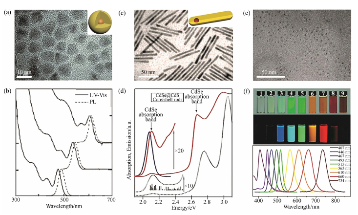
图 2 3种量子点透射电镜照片及其吸收/荧光光谱图。(a)和(b) CdSe量子点[15];(c)和(d) CdSe@CdS点棒[31];(e)和(f) CH3NH3PbX3量子点及其在自然光和紫外光下的照片[23]
Figure 2. Transmission electron microscopy images and absorption/fluorescence spectra of three kinds of quantum dots. (a), (b) CdSe quantum dots[15]; (c), (d) CdSe@CdS core/shell rods[31]; (e), (f) CH3NH3PbX3 quantum dots and photograph under natural and ultraviolet light[23]


表 1 CCD与CMOS成像器件关键参数对比
Table 1. Comparison of key parameters for CCD and CMOS
关键参数 CCD CMOS 像素信号 电荷包 电压 芯片信号 模拟电压 比特(数字) 灵敏度 高 较高 动态范围 高 中至高 一致性 高 稍微较低 成本 较高 较低  下载: 导出CSV
-
[1] 王俊.超级像素CMOS图像传感器技术研究[D].上海: 中国科学院研究生院(上海技术物理研究所), 2014.WANG J. Research on superpixel CMOS image sensor technology[D]. Shanghai: University of Chinese Academy of Sciences (Shanghai Institute of Technical Physics) 2014. (in Chinese) [2] MURAMATSU M, AKAHORI H, SHIBAYAMA K, et al.Greater-than-90% QE in visible spectrum perceptible from UV to near-IR Hamamatsu thinned back-illuminated CCDs[J]. Proceedings of SPIE, 1997, 3019: 2-8. doi: 10.1117/12.275165 [3] ALIVISATOS A P. Semiconductor clusters, Nanocrystals, and quantum dots[J]. Science, 1996, 271(5251): 933-937. doi: 10.1126/science.271.5251.933 [4] CARUGE J M, HALPERT J E, WOOD V, et al.Colloidal quantum-dot light-emitting diodes with metal-oxide charge transport layers[J]. Nature Photonics, 2008, 2(4): 247-250. doi: 10.1038/nphoton.2008.34 [5] TAN ZH K, MOGHADDAM R S, LAI M L, et al.Bright light-emitting diodes based on organometal halide perovskite[J]. Nature Nanotechnology, 2014, 9(9): 687-692. doi: 10.1038/nnano.2014.149 [6] KONSTANTATOS G, HOWARD I, FISCHER A, et al.Ultrasensitive solution-cast quantum dot photodetectors[J]. Nature, 2006, 442(7099): 180-183. doi: 10.1038/nature04855 [7] MEDINTZ I L, UYEDA H T, GOLDMAN E R, et al.Quantum dot bioconjugates for imaging, labelling and sensing[J]. Nature Materials, 2005, 4(6): 435-446. doi: 10.1038/nmat1390 [8] SAHU S, BEHERA B, MAITI T K, et al.Simple one-step synthesis of highly luminescent carbon dots from orange juice: application as excellent bio-imaging agents[J]. Chemical Communications, 2012, 48(70): 8835-8837. doi: 10.1039/c2cc33796g [9] SHEN J H, ZHU Y H, YANG X L, et al.Graphene quantum dots: emergent nanolights for bioimaging, sensors, catalysis and photovoltaic devices[J]. Chemical Communications, 2012, 48(31): 3686-3699. doi: 10.1039/c2cc00110a [10] LI H T, HE X D, KANG ZH H, et al.Water-soluble fluorescent carbon quantum dots and photocatalyst design[J]. Angewandte Chemie International Edition, 2010, 49(26): 4430-4434. doi: 10.1002/anie.200906154 [11] MURRAY C B, NORRIS D J, BAWENDI M G. Synthesis and characterization of nearly monodisperse CdE (E = sulfur, selenium, tellurium) semiconductor nanocrystallites[J]. Journal of the American Chemical Society, 1993, 115(19): 8706-8715. doi: 10.1021/ja00072a025 [12] PENG Z A, PENG X G. Formation of high-quality CdTe, CdSe, and CdS nanocrystals using CdO as precursor[J]. Journal of the American Chemical Society, 2001, 123(1): 183-184. doi: 10.1021/ja003633m [13] QU L H, PENG Z A, PENG X G. Alternative routes toward high quality CdSe nanocrystals[J]. Nano Letters, 2001, 1(6): 333-337. doi: 10.1021/nl0155532 [14] YU W W, PENG X G. Formation of high-quality CdS and other Ⅱ-VI semiconductor nanocrystals in noncoordinating solvents: tunable reactivity of monomers[J]. Angewandte Chemie International Edition, 2002, 41(13): 2368-2371. doi: 10.1002/1521-3773(20020703)41:13<2368::AID-ANIE2368>3.0.CO;2-G [15] YU W W, QU L H, GUO W ZH, et al.Experimental determination of the extinction coefficient of CdTe, CdSe, and CdS nanocrystals[J]. Chemistry of Materials, 2003, 15(14): 2854-2860. doi: 10.1021/cm034081k [16] BATTAGLIA D, PENG X G. Formation of high quality InP and InAs nanocrystals in a noncoordinating solvent[J]. Nano Letters, 2002, 2(9): 1027-1030. doi: 10.1021/nl025687v [17] CROS-GAGNEUX A, DELPECH F, NAYRAL C, et al.Surface chemistry of InP quantum dots: a comprehensive study[J]. Journal of the American Chemical Society, 2010, 132(51): 18147-18157. doi: 10.1021/ja104673y [18] HARRIS D K, BAWENDI M G. Improved precursor chemistry for the synthesis of Ⅲ-Ⅴ quantum dots[J]. Journal of the American Chemical Society, 2012, 134(50): 20211-20213. doi: 10.1021/ja309863n [19] HINES M A, SCHOLES G D. Colloidal PbS nanocrystals with size-tunable near-infrared emission: observation of post-synthesis self-narrowing of the particle size distribution[J]. Advanced Materials, 2003, 15(21): 1844-1849. doi: 10.1002/adma.200305395 [20] MCDONALD S A, KONSTANTATOS G, ZHANG SH G, et al.Solution-processed PbS quantum dot infrared photodetectors and photovoltaics[J]. Nature Materials, 2005, 4(2): 138-142. doi: 10.1038/nmat1299 [21] MOREELS I, LAMBERT K, SMEETS D, et al.Size-dependent optical properties of colloidal PbS quantum dots[J]. ACS Nano, 2009, 3(10): 3023-3030. doi: 10.1021/nn900863a [22] PROTESESCU L, YAKUNIN S, BODNARCHUK M I, et al.Nanocrystals of cesium lead halide perovskites (CsPbX3, X= Cl, Br, and I): novel optoelectronic materials showing bright emission with wide color gamut[J]. Nano letters, 2015, 15(6): 3692-3696. doi: 10.1021/nl5048779 [23] ZHANG F, ZHONG H ZH, CHEN CH, et al.Brightly luminescent and color-tunable colloidal CH3NH3PbX3 (X = Br, I, Cl) quantum dots: potential alternatives for display technology[J]. ACS Nano, 2015, 9(4): 4533-4542. doi: 10.1021/acsnano.5b01154 [24] SONG J ZH, LI J H, LI X M, et al.Quantum dot light-emitting diodes based on inorganic perovskite cesium lead halides (CsPbX3)[J]. Advanced Materials, 2015, 27(44): 7162-7167. doi: 10.1002/adma.201502567 [25] ZHOU Q CH, BAI Z L, LU W G, et al.In situ fabrication of halide perovskite nanocrystal-embedded polymer composite films with enhanced photoluminescence for display backlights[J]. Advanced Materials, 2016, 28(41): 9163-9168. doi: 10.1002/adma.201602651 [26] CHEN N J, BAI Z L, WANG Z M, et al.P-119: low cost perovskite quantum dots film based wide color gamut backlight unit for LCD TVs[J]. SID Symposium Digest of Technical Papers, 2018, 49(1): 1657-1659. doi: 10.1002/sdtp.12303 [27] ZHANG M J, WANG L X, MENG L H, et al.Perovskite quantum dots embedded composite films enhancing UV response of silicon photodetectors for broadband and solar-blind light detection[J]. Advanced Optical Materials, 2018, 6(16): 1800077. doi: 10.1002/adom.201800077 [28] TAN Q W, WU X G, ZHANG M J, et al.Performance analysis of PQDCF-coated silicon image sensor using Monte-Carlo ray-trace simulation[J]. Optics Express, 2019, 27(6): 9079-9087. doi: 10.1364/OE.27.009079 [29] LU W G, WU X G, HUANG S, et al.Strong polarized photoluminescence from stretched perovskite-nanocrystal-embedded polymer composite films[J]. Advanced Optical Materials, 2017, 5(23): 1700594. doi: 10.1002/adom.201700594 [30] WANG L, MENG L H, CHEN L, et al.Ultralow-threshold and color-tunable continuous-wave lasing at room-temperature from in-situ fabricated perovskite quantum dots[J]. The Journal of Physical Chemistry Letters, 2019, 10(12): 3248-3253. doi: 10.1021/acs.jpclett.9b00658 [31] CARBONE L, NOBILE C, DE GIORGI M, et al.Synthesis and micrometer-scale assembly of colloidal CdSe/CdS nanorods prepared by a seeded growth approach[J]. Nano Letters, 2007, 7(10): 2942-2950. doi: 10.1021/nl0717661 [32] NIRMAL M, NORRIS D J, KUNO M, et al.Observation of the "dark exciton" in CdSe quantum dots[J]. Physical Review Letters, 1995, 75(20): 3728-3731. doi: 10.1103/PhysRevLett.75.3728 [33] MENDE S B, HEETDERKS H, FREY H U, et al.Far ultraviolet imaging from the IMAGE spacecraft. 1. System design[J]. Space Science Reviews, 2000, 91(1-2): 243-270. http://www.wanfangdata.com.cn/details/detail.do?_type=perio&id=01d4edca421803481713b5fa5c7682a5 [34] 周峰, 郑国宪, 闫锋, 等.天基紫外预警技术发展现状及思考[J].航天返回与遥感, 2012, 33(6): 39-44. http://d.old.wanfangdata.com.cn/Periodical/htfhyyg201206007ZHOU F, ZHENG G X, YAN F, et al.Development status and thoughts of space-based UV warning technology[J]. Spacecraft Recovery & Remote Sensing, 2012, 33(6): 39-44. (in Chinese) http://d.old.wanfangdata.com.cn/Periodical/htfhyyg201206007 [35] ØSTERGAARD J. UV imaging in pharmaceutical analysis[J]. Journal of Pharmaceutical and Biomedical Analysis, 2018, 147: 140-148. doi: 10.1016/j.jpba.2017.07.055 [36] NIKZAD S, HOENK M E, GREER F, et al.Delta-doped electron-multiplied CCD with absolute quantum efficiency over 50% in the near to far ultraviolet range for single photon counting applications[J]. Applied Optics, 2012, 51(3): 365-369. doi: 10.1364/AO.51.000365 [37] HAMDEN E T, GREER F, HOENK M E, et al.Ultraviolet antireflection coatings for use in silicon detector design[J]. Applied Optics, 2011, 50(21): 4180-4188. doi: 10.1364/AO.50.004180 [38] KARCHER A, BEBEK C J, KOLBE W F, et al.Measurement of lateral charge diffusion in thick, fully depleted, back-illuminated CCDs[C]. Proceedings of 2003 IEEE Nuclear Science Symposium, IEEE, 2003: 1513-1517. [39] KNOWLES A, WILLIAMS S, NINKOV Z, et al.Incorporating quantum dots in a magnesium fluoride matrix to enable deep-UV sensitivity for standard silicon based imaging detectors[J]. Proceedings of SPIE, 2019, 10982: 1098234. http://cn.bing.com/academic/profile?id=bc33ff969cdb1b9016104c66ddf6f734&encoded=0&v=paper_preview&mkt=zh-cn [40] SHENG X, YU C J, MALYARCHUK V, et al.Silicon-based visible-blind ultraviolet detection and imaging using down-shifting luminophores[J]. Advanced Optical Materials, 2014, 2(4): 314-319. doi: 10.1002/adom.201300475 [41] MORRISSEY P F, MCCANDLISS S R, FELDMAN P D, et al.Ultraviolet performance of a lumigen-coated CCD[J]. Bulletin of the American Astronomical Society, 1991, 23: 1316. https://www.researchgate.net/publication/234265441_Ultraviolet_Performance_of_a_Lumigen-Coated_CCD [42] DESLANDES A, WEDDING A B, CLARKE S R, et al.Characterization of PVD lumogen films for wavelength conversion applications[J]. Proceedings of SPIE, 2005, 5649: 616-626. doi: 10.1117/12.582244 [43] 刘猛, 张大伟, 谢品, 等.增强光电图像传感器紫外探测薄膜的制备[J].仪表技术与传感器, 2009(9): 12-14. doi: 10.3969/j.issn.1002-1841.2009.09.005LIU M, ZHANG D W, XIE P, et al.Investigation in UV-enhanced coatings based on Zn2SiO4: Mn for image sensors[J]. Instrument Technique and Sensor, 2009(9): 12-14. (in Chinese) doi: 10.3969/j.issn.1002-1841.2009.09.005 [44] FRANKS W A R, KⅡK M J, NATHAN A. UV-responsive CCD image sensors with enhanced inorganic phosphor coatings[J]. IEEE Transactions on Electron Devices, 2003, 50(2): 352-358. doi: 10.1109/TED.2003.809029 [45] ROBINSON R, NINKOV Z, CORMIER D, et al.First report on quantum dot coated CMOS CID arrays for the UV and VUV[J]. Proceedings of SPIE, 2013, 8859: 88590K. http://cn.bing.com/academic/profile?id=df065f252d024c43fcffe75b34b887eb&encoded=0&v=paper_preview&mkt=zh-cn [46] JIANG L, SUN H J, XU B L, et al.The spectrum of quantum dots film for UV CCD[J]. Journal of Spectroscopy, 2013: 803907. http://cn.bing.com/academic/profile?id=1e7ad462dfa0c375a1df68bc87ec6a75&encoded=0&v=paper_preview&mkt=zh-cn [47] ROGALSKI A. Infrared detectors: an overview[J]. Infrared Physics & Technology, 2002, 43(3-5): 187-210. http://d.old.wanfangdata.com.cn/Periodical/hwyhmb200706003 [48] ROGALSKI A. Recent progress in infrared detector technologies[J]. Infrared Physics & Technology, 2011, 54(3): 136-154. http://cn.bing.com/academic/profile?id=8b1cbabae30cb958a23c23df14e983b7&encoded=0&v=paper_preview&mkt=zh-cn [49] MANDELLI E, BEILEY Z M, KOLLI N, et al.Quantum dot-based image sensors for cutting-edge commercial multispectral cameras[J]. Proceedings of SPIE, 2016, 9933: 993304. http://cn.bing.com/academic/profile?id=45db81d2318e996a9b12847605162135&encoded=0&v=paper_preview&mkt=zh-cn [50] BEILEY Z M, CHEUNG R, HANELT E F, et al.Device design for global shutter operation in a 1.1-μm pixel image sensor and its application to near infrared sensing[J]. Proceedings of SPIE, 2017, 10098: 100981L. doi: 10.1117/12.2253219 [51] BEILEY Z M, PATTANTYUS-ABRAHAM A, HANELT E, et al.Design and characterization of 1.1 micron pixel image sensor with high near infrared quantum efficiency[J]. Proceedings of SPIE, 2017, 10100: 101001B. http://cn.bing.com/academic/profile?id=c834a9ff49bf2a28052be83566520b04&encoded=0&v=paper_preview&mkt=zh-cn [52] KIM H Y, YOON D E, JANG J, et al.Quantum dot/siloxane composite film exceptionally stable against oxidation under heat and moisture[J]. Journal of the American Chemical Society, 2016, 138(50): 16478-16485. doi: 10.1021/jacs.6b10681 [53] SUÁREZ I, GORDILLO H, ABARGUES R, et al.Photoluminescence waveguiding in CdSe and CdTe QDs-PMMA nanocomposite films[J]. Nanotechnology, 2011, 22(43): 435202. doi: 10.1088/0957-4484/22/43/435202 [54] TYO J S, GOLDSTEIN D L, CHENAULT D B, et al.Review of passive imaging polarimetry for remote sensing applications[J]. Applied Optics, 2006, 45(22): 5453-5469. doi: 10.1364/AO.45.005453 [55] VERMA V B, MARSILI F, HARRINGTON S, et al.A three-dimensional, polarization-insensitive superconducting nanowire avalanche photodetector[J]. Applied Physics Letters, 2012, 101(25): 251114. doi: 10.1063/1.4768788 [56] CREMER F, DE JONG W, SCHUTTE K. Infrared polarization measurements and modelling applied to surface laid anti-personnel landmines[J]. Optical Engineering, 2002, 41(5): 1021-1032. doi: 10.1117/1.1467362 [57] GE Y, ZHANG M J, WANG L, et al.Polarization-sensitive ultraviolet detection from oriented-CdSe@CdS-dot-in-rods-integrated silicon photodetector[J]. Advanced Optical Materials, 2019, 7(18): 1900330. doi: 10.1002/adom.201900330 [58] CHAGANTI K, SALAKHUTDINOV I, AVRUTSKY I, et al.A simple miniature optical spectrometer with a planar waveguide grating coupler in combination with a plano-convex lens[J]. Optics Express, 2006, 14(9): 4064-4072. doi: 10.1364/OE.14.004064 [59] JANSEN-VAN VUUREN R D, ARMIN A, PANDEY A K, et al.Organic photodiodes: the future of full color detection and image sensing[J]. Advanced Materials, 2016, 28(24): 4766-4802. doi: 10.1002/adma.201505405 [60] WOLFFENBUTTEL R F. State-of-the-art in integrated optical microspectrometers[J]. IEEE Transactions on Instrumentation and Measurement, 2004, 53(1): 197-202. doi: 10.1109/TIM.2003.821490 [61] MCGONIGLE A J S, WILKES T C, PERING T D, et al.Smartphone spectrometers[J]. Sensors, 2018, 18(1): 223. doi: 10.1109/JSEN.2017.2765745 [62] BACON C P, MATTLEY Y, DEFRECE R. Miniature spectroscopic instrumentation: applications to biology and chemistry[J]. Review of Scientific Instruments, 2004, 75(1): 1-16. doi: 10.1063/1.1633025 [63] CHIN C D, LINDER V, SIA S K. Lab-on-a-chip devices for global health: past studies and future opportunities[J]. Lab on a Chip, 2007, 7(1): 41-57. doi: 10.1039/B611455E [64] KONG S H, WIJNGAARDS D D L, WOLFFENBUTTEL R F. Infrared micro-spectrometer based on a diffraction grating[J]. Sensors and Actuators A: Physical, 2001, 92(1-3): 88-95. doi: 10.1016/S0924-4247(01)00544-1 [65] GOLDMAN D S, WHITE P L, ANHEIER N C. Miniaturized spectrometer employing planar waveguides and grating couplers for chemical analysis[J]. Applied Optics, 1990, 29(31): 4583-4589. doi: 10.1364/AO.29.004583 [66] BRYAN K M, JIA ZH, PERVEZ N K, et al.Inexpensive photonic crystal spectrometer for colorimetric sensing applications[J]. Optics Express, 2013, 21(4): 4411-4423. doi: 10.1364/OE.21.004411 [67] WANG SH W, XIA CH SH, CHEN X SH, et al.Concept of a high-resolution miniature spectrometer using an integrated filter array[J]. Optics Letters, 2007, 32(6): 632-634. doi: 10.1364/OL.32.000632 [68] DUEMPELMANN L, GALLINET B, NOVOTNY L. Multispectral imaging with tunable plasmonic filters[J]. ACS Photonics, 2017, 4(2): 236-241. doi: 10.1021/acsphotonics.6b01003 [69] KUMAR K, DUAN H G, HEGDE R S, et al.Printing colour at the optical diffraction limit[J]. Nature Nanotechnology, 2012, 7(9): 557-561. doi: 10.1038/nnano.2012.128 [70] BAO J, BAWENDI M G. A colloidal quantum dot spectrometer[J]. Nature, 2015, 523(7558): 67-70. doi: 10.1038/nature14576 [71] KHAN S A, BOWDEN A K E. Colloidal quantum dots for cost-effective, miniaturized, and simple spectrometers[J]. Clinical Chemistry, 2016, 62(4): 548-550. doi: 10.1373/clinchem.2015.247999 -

 下载:
下载:


图(7) / 表(1)
计量
- 文章访问数: 4512
- HTML全文浏览量: 2359
- PDF下载量: 291
- 被引次数: 0
