


Intermixing in InGaAs/AlGaAs quantum well structures induced by the interdiffusion of Si impurities
-
摘要: 光学灾变损伤(COD)常发生于量子阱半导体激光器的前腔面处,极大地影响了激光器的出光功率及寿命。通过杂质诱导量子阱混杂技术使腔面区波长蓝移来制备非吸收窗口是抑制腔面COD的有效手段,也是一种高效率、低成本方法。本文选择了Si杂质作为量子阱混杂的诱导源,使用金属有机化学气相沉积设备生长了InGaAs/AlGaAs量子阱半导体激光器外延结构、Si杂质扩散层及Si3N4保护层。热退火处理后,Si杂质扩散诱导量子阱区和垒区材料互扩散,量子阱禁带变宽,输出波长发生蓝移。退火会影响外延片的表面形貌,而表面形貌则可能会影响后续封装工艺中电极的制备。结合光学显微镜及光致发光谱的测试结果,得到825℃/2 h退火条件下约93 nm的最大波长蓝移量,也证明退火对表面形貌的改变,不会影响波长蓝移效果及后续电极工艺。Abstract: Catastrophe Optical Damage (COD) usually occurs at the front cavity surface of quantum well semiconductor laser diodes, and it is a great trouble to its output power and life. The preparation of Non-Absorption Window (NAW) by quantum well intermixing based on Impurity Induced Disordering (IID) is a common method for inhibiting COD at the cavity surface, which has a great potential to achieve blue shift with high efficiency and low cost. In this paper, Si impurities were used to induce quantum well intermixing. The epitaxial structure of the InGaAs/AlGaAs quantum well semiconductor laser diode and the Si impurity diffusion layer and Si3N4 protective layer were grown by a Metal Organic Chemical Vapor Deposition (MOCVD) device. After several thermal annealing treatments, the Si impurity diffusion inducing the mutual diffusion between the quantum well and the barrier, which widened the band gap of the quantum well area and resulted in blue shift of the output wavelength, reducing the absorption of the emitted light. Usually thermal annealing will affect the surface morphology of epitaxial surface, and the surface morphology may affect the preparation of electrode in the subsequent packaging process. Combined with an optical microscope and photoluminescence (PL) spectrum, experimental results indicate that about 93nm wavelength blue shift can be observed under the annealing condition of 825℃/2 h. In conclusion, annealing can affect the topography of the epitaxial wafer's surface, but it does not affect the blue shift of wavelength and the preparation of electrode.
-
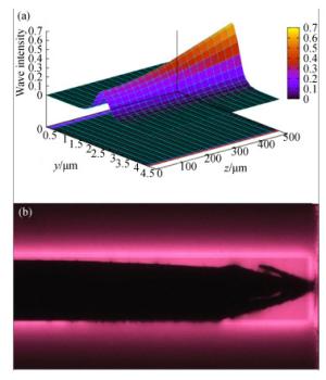
图 1 半导体激光器的腔面COD现象。(a)PICS3D软件模拟所得芯片沿腔长方向的二维光强分布; (b) EL测试中产生的前腔面COD现象
Figure 1. (Color online)COD phenomenon at the cavity surface of LD. (a) Distribution of 2D optical intensity profile along the direction of cavity length simulated by PICS3D; (b) COD phenomenon of the front cavity surface in EL test
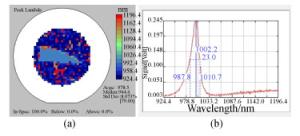
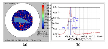
图 4 InGaAs/AlGaAs量子阱激光器的PL谱测试结果。(a)芯片PL谱Mapping结果; (b)芯片PL谱
Figure 4. PL spectrum of chip. (a) The mapping results of PL testing; (b) PL spectrum of chip
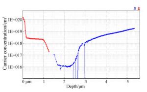
图 5 InGaAs/AlGaAs量子外延层的ECV测试结果
Figure 5. ECV test results of InGaAs/AlGaAs quantum epitaxial layer
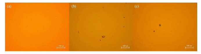
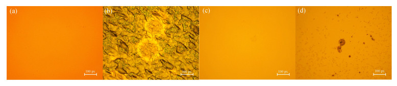
图 6 A-si组样品RTA前后的表面形貌。(a)退火前; (b)850℃/120s快速热退火; (c)有GaAs盖片,850℃/120s快速热退火
Figure 6. Surface morphologies of group A-Si samples before and after RTA. (a) Before RTA; (b) after RTA at 850 ℃/120s; (c) with GaAs cover after RTA at 850℃/120s

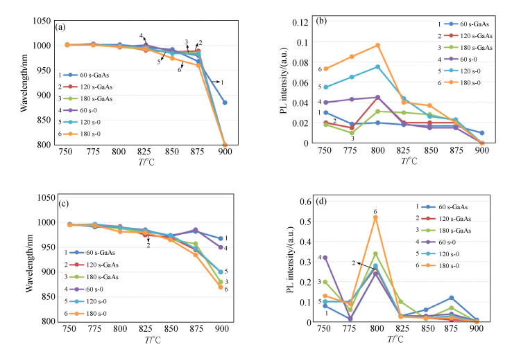
图 7 A组样品RTA后的PL谱测试结果。(a)A-0组样品RTA后的中心波长; (b)A-0组样品RTA后的发光强度; (c)A-Si组样品RTA后的中心波长; (d)A-Si组样品RTA后的发光强度
Figure 7. PL spectra of group A samples after RTA. (a) The central wavelength of A-0 samples after RTA; (b) the intensity of A-0 samples after RTA; (c) the central wavelength of A-Si samples after RTA; (d) the intensity of A-Si samples after RTA
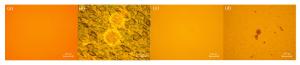
图 8 B组样品退火前后的表面形貌。(a)B-0组样品,无退火; (b)B-0组样品,850℃/1h退火; (c)B-si组,无退火; (d)B-si组样品,850℃/1 h退火
Figure 8. Surface morphology of group B samples before and after annealing. (a) B-0 samples before annealing; (b) B-0 samples after annealing at 850℃/1 h; (c) B-Si samples before annealing; (d) B-Si samples after annealing at 850℃/1h
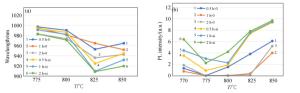
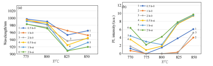
图 9 B组样品退火后的PL谱测试结果。(a)退火后的中心波长; (b)退火后的发光强度
Figure 9. PL spectra of group B samples after annealing. (a) The central wavelength after annealing; (b) The intensity after annealing
表 1 InGaAs/AlGaAs量子阱激光器的外延结构及相应参数
Table 1. Epitaxial structure and parameters of InGaAs/AlGaAs QW LD
NO. Layer Material Composition Thickness Dopant 13 contract P-GaAs _ 150 nm C/P++ 12 grin p-AlxGaAs 0.37-0.1 67 nm C/P+ 11 cladding p-AlxGaAs 0.37 1100 nm C/P 10 grin p-AlxGaAs 0.255-0.37 120nm C/P 9 upper waveguide p-AlxGaAs 0.255 380 nm C/P 8 grin p-AlxGaAs 0.1-0.255 30 nm Un. 7 QW InxGaAs 0.267 7.4 nm Un. 6 grin n-AlxGaAs 0.255-0.1 30 nm Un. 5 lower waveguide n-AlxGaAs 0.255 800 nm Si/N 4 grin n-AlxGaAs 0.31-0.255 100 nm Si/N 3 cladding n-AlxGaAs 0.31 1460 nm Si/N 2 buffer n-GaAs _ 500 nm Si/N 1 substrate n-GaAs _ 450 μm  下载: 导出CSV
-
[1] 戴银, 李林, 苑汇帛, 等. InGaAs/GaAs应变量子阱的发光特性研究[J].光学学报, 2014, 34(11): 1131001. http://www.wanfangdata.com.cn/details/detail.do?_type=perio&id=gxxb201411050DAI Y, LI L, YUAN H B, et al.. Research on photoluminescence properties of InGaAs/GaAs strained quantum well[J]. Acta Optica Sinica, 2014, 34(11): 1131001. (in Chinese) http://www.wanfangdata.com.cn/details/detail.do?_type=perio&id=gxxb201411050 [2] JIA Y, YU Q N, LI F, et al.. Experimental investigation of loss and gain characteristics of an abnormal InxGa1-xAs/GaAs quantum well structure[J]. Chinese Optics Letters, 2018, 16(1): 011402. doi: 10.3788/COL201816.011402 [3] GU L, LI L, QIAO ZH L, et al.. High-strain InGaAs/GaAs quantum well grown by MOCVD[J]. Chinese Optics Letters, 2014, 12(10): 102702. doi: 10.3788/COL201412.102702 [4] 霍大云, 石震武, 张伟, 等. InGaAs/AlGaAs量子阱红外探测器中势垒生长温度的研究[J].物理学报, 2017, 66(6): 068501. http://www.wanfangdata.com.cn/details/detail.do?_type=perio&id=wlxb201706038HUO D Y, SHI ZH W, ZHANG W, et al.. Barrier growth temperature of InGaAs/AlGaAs-quantum well infrared photodetector[J]. Acta Physica Sinica, 2017, 66(6): 068501. (in Chinese) http://www.wanfangdata.com.cn/details/detail.do?_type=perio&id=wlxb201706038 [5] 仇伯仓, 胡海, 汪卫敏, 等. 12 W高功率高可靠性915 nm半导体激光器设计与制作[J].中国光学, 2018, 11(4): 590-603. http://www.chineseoptics.net.cn/CN/abstract/abstract9620.shtmlQIU B C, HU H, WANG W M, et al.. Design and fabrication of 12 W high power and high reliability 915 nm semiconductor lasers[J]. Chinese Optics, 2018, 11(4): 590-603. (in Chinese) http://www.chineseoptics.net.cn/CN/abstract/abstract9620.shtml [6] 林盛杰, 李建军, 何林杰, 等.基于循环退火技术的InGaAs/AlGaAs量子阱混杂[J].光电子·激光, 2014, 25(8): 1471-1475. http://www.wanfangdata.com.cn/details/detail.do?_type=perio&id=gdzjg201408006LIN SH J, LI J J, HE L J, et al.. Enhanced AlGaAs/InGaAs quantum well intermixing by the technology of cycles annealing[J]. Journal of Optoelectronics·Laser, 2014, 25(8): 1471-1475. (in Chinese) http://www.wanfangdata.com.cn/details/detail.do?_type=perio&id=gdzjg201408006 [7] MEI P, YOON H W, VENKATESAN T, et al.. Kinetics of silicon-induced mixing of AlAs-GaAs superlattices[J]. Applied Physics Letters, 1987, 50(25): 1823-1825. doi: 10.1063/1.97709 [8] CONG G W, AKIMOTO R, GOZU S, et al.. Simultaneous generation of intersubband absorption and quantum well intermixing through silicon ion implantation in undoped InGaAs/AlAsSb coupled double quantum wells[J]. Applied Physics Letters, 2010, 96(10): 101901. doi: 10.1063/1.3357433 [9] 彭海涛.用量子阱混合技术提高大功率半导体激光器腔面的COD阈值[D].天津: 河北工业大学, 2007. http://kns.cnki.net/KCMS/detail/detail.aspx?dbcode=CMFD&filename=2008156781.nhPENG H T. Improving the COD level of high-power semiconductor lasers using quantum well intermixing[D]. Tianjin: Hebei University of Technology, 2007. (in Chinese) http://kns.cnki.net/KCMS/detail/detail.aspx?dbcode=CMFD&filename=2008156781.nh [10] SHINDE S S, BHOSALE C H, RAJPURE K Y. Solar light assisted photocatalysis of water using a zinc oxide semiconductor[J]. Journal of Semiconductors, 2013, 34(4): 043002. doi: 10.1088/1674-4926/34/4/043002 [11] 周路.高功率半导体激光器抗COD关键技术研究[D].长春: 长春理工大学, 2014. http://cdmd.cnki.com.cn/Article/CDMD-10186-1014186073.htmZHOU L. Research on anti catastrophic optical damage of high power semiconductor laser diodes[D]. Changchun: Changchun University of Science and Technology, 2014. (in Chinese) http://cdmd.cnki.com.cn/Article/CDMD-10186-1014186073.htm [12] ZHAO J Y, GUO J, HUANG X D, et al.. Spatial control based quantum well intermixing in InP/InGaAsP structures using ICP[J]. Journal of Semiconductors ,2012, 33(10): 106001. doi: 10.1088/1674-4926/33/10/106001 [13] TIAN W N, XIONG C, WANG X, et al.. Impurity-free vacancy diffusion induces intermixing in GaInP/AlGaInP quantum wells using GaAs encapsulation[J]. Chinese Journal of Luminescence, 2018, 39(8): 1095-1099. doi: 10.3788/fgxb20183908.1095 [14] 王鑫, 赵懿昊, 朱凌妮, 等.基于SiO2薄膜的915 nm半导体激光器的无杂质空位诱导量子阱混合研究[J].光子学报, 2018, 47(3): 94-100. http://www.wanfangdata.com.cn/details/detail.do?_type=perio&id=gzxb201803013WANG X, ZHAO Y H, ZHU L N, et al.. Impurity-free vacancy diffusion induces quantum well intermixing in 915 nm semiconductor laser based on SiO2 film[J]. Acta Photonica Sinica, 2018, 47(3): 94-100. (in Chinese) http://www.wanfangdata.com.cn/details/detail.do?_type=perio&id=gzxb201803013 [15] LEE J, DOIK, HIRATANI T, et al.. High quality quantum-well intermixing for InP-based membrane photonic integration on Si[C]. Proceedings of the 26th International Conference on Indium Phosphide and Related Materials, IEEE, 2014: 1-2. https://www.researchgate.net/publication/271466422_High_quality_quantum-well_intermixing_for_InP-based_membrane_photonic_integration_on_Si [16] DEPPE D G, HOLONYAK JR N. Atom diffusion and impurity-induced layer disordering in quantum well Ⅲ-V semiconductor heterostructures[J]. Journal of Applied Physics, 1988, 64(12): R93-R113. doi: 10.1063/1.341981 [17] 方小华, 鲍希茂. GaAs中Si扩散机制的研究[J].半导体学报, 1996, 17(12): 919-922. doi: 10.3321/j.issn:0253-4177.1996.12.008FANG X H, BAO X M. Study on mechanism of Si diffusion in GaAs[J]. Chinese Journal of Semiconductors, 1996, 17(12): 919-922. (in Chinese) doi: 10.3321/j.issn:0253-4177.1996.12.008 -

 下载:
下载:


计量
- 文章访问数: 2711
- HTML全文浏览量: 861
- PDF下载量: 121
- 被引次数: 0
