Electron transfer mechanism of butylamine-capped CdSe quantum dot sensitized nanocrystalline TiO2 films
-
摘要: 利用超快光谱技术系统研究了在丁胺包裹的CdSe量子点敏化的TiO2纳米晶薄膜起始时刻界面间电子转移动力学。与之前的报道不同,该实验结果表明:CdSe量子点经过表面修饰后,两相电子注入机制——热电子和冷电子注入得以被证实,即:电子能分别从CdSe量子点导带中高的振动能级和导带底转移到TiO2的导带。该机制详细描绘了电子在纳米界面间转移的图景。进一步研究发现:热电子注入的电子耦合强度(3.6±0.1 meV)比弛豫后的基态电子注入高两个数量级,基于Marcus理论,伴随着0.083 eV的重组能,冷电子注入的耦合强度值为~50 μeV。Abstract: In this paper, we have investigated the initial interfacial electron transfer dynamics in butylamine-capped CdSe quantum dot(QD)-sensitized nanocrystalline TiO2 films by ultrafast spectroscopy. Different with previous reports, the experiment results indicate that after surface modification of CdSe QDs, a two-phase electron injection mechanism(hot and cold electron injection) is validated, namely, electrons transfer from high vibration energy levels in conduction band and conduction band bottom of CdSe quantum dots into conduction band of TiO2, respectively. This mechanism depicts a picture on the detailed charge transfer processes at the nano interfaces. We further find that the electron coupling strength (3.6±0.1 meV) of hot electron injection is two orders of magnitude larger than that of relaxed ground-state electron injection, which gives a value of ~50 μeV accompanied with reorganization energy 0.083 eV on the basis of Marcus theory.
-
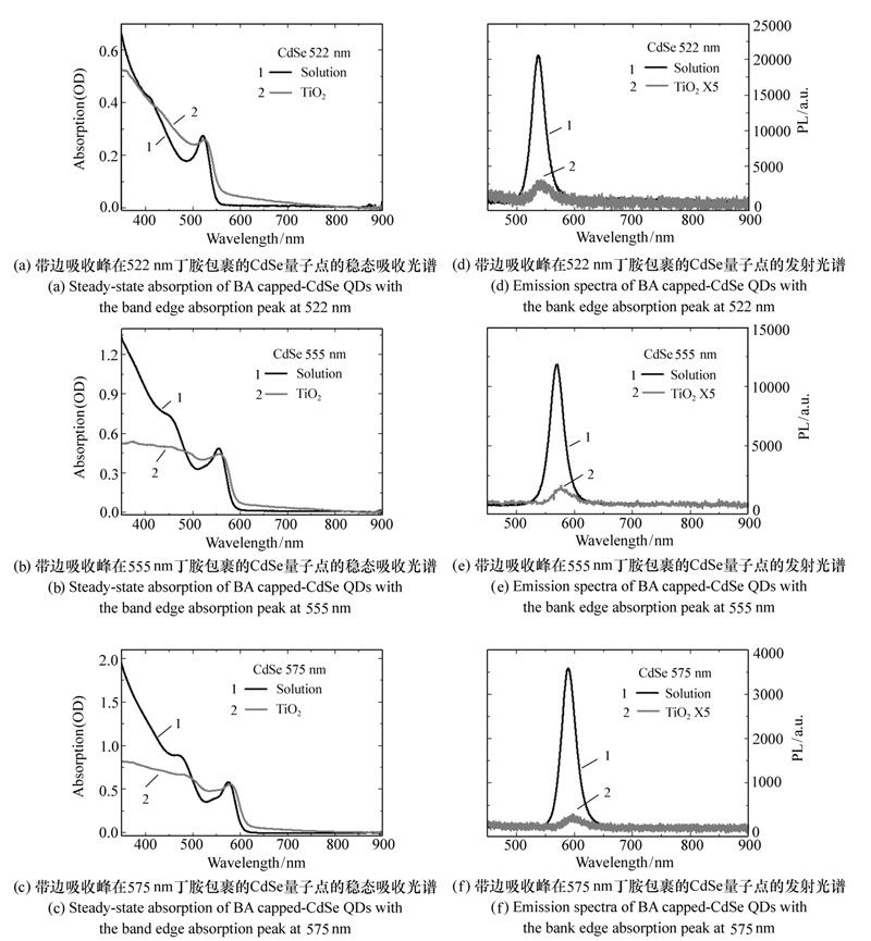
图 1 带边吸收峰分别在522 nm、555 nm和 575 nm处的3种丁胺包裹的CdSe量子点的稳态吸收光谱和相应的发射光谱。曲线1和曲线2分别代表在溶液中和敏化在TiO2纳米晶薄膜上的量子点
Figure 1. Steady-state absorption and emission spectra of three kinds of BA capped-CdSe QDs with the band edge absorption peak at 522 nm,555 nm,575 nm,respectively. The curve 1 represents the QDs in solution and the curve 2 represents the QDs sensitized on TiO2 nanocrystalline films
图 2 带边吸收峰在522 nm、555 nm和 575 nm处的3种丁胺包裹的CdSe量子点它们分别在溶液中(a)、(b)、(c)和敏化在TiO2纳米晶薄膜上(d)、(e)、(f)的瞬态吸收光谱
Figure 2. Transient absorption spectra of three kinds of BA capped-CdSe QDs with the band edge absorption peak at 522 nm,555 nm,575 nm in solution (a),(b),(c) and those sensitized on TiO2 nanocrystalline films (d),(e),(f)
图 3 (a)、(b)、(c)分别展示了带边吸收峰在522 nm、[JP]555 nm和 575 nm处的3种丁胺包裹的CdSe量子点在光激发后前2 ps基态态填充信号的归一化动力学。方块线和圆点线分别代表在溶液中和敏化在TiO2纳米晶薄膜上的量子点
Figure 3. Normalized kinetics of ground state state-filling signals of three kinds of BA capped-CdSe QDs with the band edge absorption peak at 522 nm,555 nm,575 nm during the first 2 ps following photoexcitation are shown in (a),(b),(c). The square lines represent the QDs in solution(black) and the round dot lines represent the QDs sensitized on TiO2 nanocrystalline films
图 4 (a)、(b)、(c)分别展示了带边吸收峰在522 nm、555 nm和 575 nm处的3种丁胺包裹的CdSe量子点在光激发之后前6 ps的基态态填充信号的归一化动力学,曲线1和曲线2分别代表在溶液中和旋涂在石英衬底上的量子点
Figure 4. Normalized kinetics of ground state state-filling signals of three kinds of BA capped-CdSe QDs with the band edge absorption peak at 522 nm,555 nm,575 nm during the first 6 ps following photoexcitation are shown in (a),(b),(c). The curve 1 represents the QDs in solution and the curve 2 represents the QDs spuncasted on quartz substrate
图 6 (a)、(b)、(c)分别展示了带边吸收峰在522 nm、555 nm和575 nm处的3种丁胺包裹的CdSe量子点敏化的TiO2纳米晶薄膜归一化的荧光发射衰减轨迹(圈1)。曲线2代表利用模型进行的动力学拟合
Figure 6. Normalized emission decay trace(circle 1) for three kinds of BA-capped CdSe QD with the band edge absorption peak at 522 nm,555 nm,575 nm sensitized TiO2 films are shown in (a),(b),(c). The curve 2 represents the kinetic fit by the model
表 1 瞬态吸收光谱测量下的基态动力学的多指数分析
Table 1. Multiple exponential analyses for ground state kinetics measured by transient absorption spectroscopy
表 2 驱动力和电子注入速率常数
Table 2. Driving force and electron jnjection rate constants
-
[1] [2] [3] [4] [5] [6] [7] [8] [9] [10] [11] [12] [13] [14] [15] [16] [17] [18] [19] [20] [21] [22] [23] [24] [25] [26] [27] [28] -


 下载:
下载:


