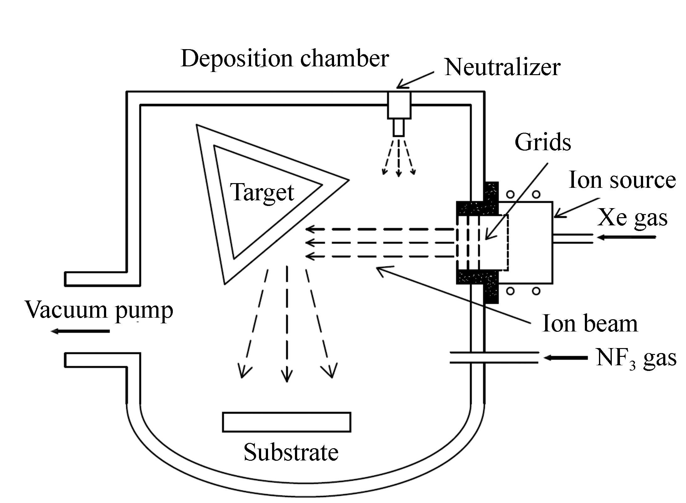
-
摘要: 采用离子束溅射制备了AlF3、GdF3单层膜及193 nm减反和高反膜系,分别使用分光光度计、原子力显微镜和应力仪研究了薄膜的光学特性、微观结构以及残余应力。在优选的沉积参数下制备出消光系数分别为1.1×10⁻⁴和3.0×10⁻⁴的低损耗AlF3和GdF3薄膜,对应的折射率分别为1.43和1.67,193 nm减反膜系的透过率为99.6%,剩余反射几乎为零,而高反膜系的反射率为99.2%,透过率为0.1%。应力测量结果表明,AlF3薄膜表现为张应力而GdF3薄膜具有压应力,与沉积条件相关的低生长应力是AlF3和GdF3薄膜残余应力较小的主要原因,采用这两种材料制备的减反及高反膜系应力均低于50 MPa。针对平面和曲率半径为240 mm的凸面元件,通过设计修正挡板,250 mm口径膜厚均匀性均优于97%。为亚纳米精度的平面元件镀制193 nm减反膜系,镀膜后RMS由0.177 nm变为0.219 nm。Abstract: AlF3, GdF3 single layers, AR and HR coatings at 193 nm were deposited by ion beam sputtering. The optical properties, microstructural properties and residual stress were investigated by spectral photometer, atomic force microscope and film stress measurement system, respectively. With proper deposition conditions, low loss AlF3, GdF3 films with the extinction coefficients of 1.1×10⁻⁴ and 3.0×10⁻⁴ can be fabricated. The corresponding refractive indexes are 1.43 and 1.67. At 193 nm, the transmittance of AR coating is 99.6% and the reflectance is almost zero. While the reflectance is 99.2% and the transmittance is 0.1% for HR coating. From the results of stress measurement, AlF3 film presents tensile stress, while GdF3 film has compressive stress. The low growing stress is the major reason for the small residual stress of AlF3 and GdF3 films. The stress of multilayer coatings consisting of these two materials is less than 50 MPa. By designing shadowing masks for a flat and a convex substrate with the radius of curvature of 240 mm, thickness uniformity of both substrates in diameter of 250 mm is better than 97%. AR coating at 193 nm was deposited on the flat substrate with sub-nanometer accuracy surface and the roughness varied from 0.177 nm RMS to 0.219 nm RMS after coating.
-
Key words:
- ion beam sputtering /
- stress /
- optical properties /
- thickness uniformity
-
图 4 (a)AlF3破裂和(d)GdF3起皱的显微镜图片,(b)和(e)对应(a)和(d)几秒后的演变,(c)和(f)是具有光滑表面的AlF3和GdF3薄膜。 (a)、(b)中标线长度为136.58 μm,(c)、(f)中标线长度为100 μm
Figure 4. Microscopic images of cracks in (a)AlF3 and wrinkles in (d)GdF3. (b) and (e) are the evolutions of (a) and (d) a few seconds later.(c) and (f) are AlF3 and GdF3 films with smooth surfaces. The label is 136.58 μm in (a) and (b),while it is 100μm in (c) and (f)
表 1 单层膜及多层膜的特征参数
Table 1. Parameters of AlF3, GdF3 films and multilayer coatings
样品 AlF3 GdF3 AR HR 厚度/nm 437.6 418.5 93.9 1565.8 光学损耗/% 0.8 1.3 0.4 0.7 表面粗糙度/nm 0.83 0.27 0.34 0.31 应力/MPa 23 -35 -20 -41 -
[1] LIU C C,LEE C C,KANEKO M,et al.. Microstructure-related properties at 193 nm of MgF2 and GdF3 films deposited by a resistive-heating boat[J]. Applied Optics,2006,45(7):1368-1374. doi: 10.1364/AO.45.001368 [2] 时光,梅林,张立超.球面元件表面AlF3薄膜的光学特性和微观结构表征[J].中国光学,2013,6(6):906-911. http://www.chineseoptics.net.cn/CN/abstract/abstract9088.shtmlSHI G,MEI L,ZHANG L CH. Characterization of optical and microstructural properties ofAlF3 thin films deposited on spherical element[J]. Chinese Optics,2013,6(6):906-911.(in Chinese) http://www.chineseoptics.net.cn/CN/abstract/abstract9088.shtml [3] ZHANG L C,CAI X K. High performance fluoride optical coatings for DUV optics[J]. SPIE,2014,9281:92810A. http://cn.bing.com/academic/profile?id=2061322383&encoded=0&v=paper_preview&mkt=zh-cn [4] LAUX S,BERNITZKI H,FASOLD D,et al.. Low-loss HR coatings on fused silica substrates for 193 nm micro-lithography applications[J]. SPIE,2008,7101:71010Y. http://cn.bing.com/academic/profile?id=1982047633&encoded=0&v=paper_preview&mkt=zh-cn [5] ULLMANN J,KERK H G,THIELSCH R,et al.. Mechanical stress in fluoride coatings[J]. SPIE,1999,3738:136-147. http://cn.bing.com/academic/profile?id=2123323099&encoded=0&v=paper_preview&mkt=zh-cn [6] GUNSTER S,DIECKMANN M,EHLERS H,et al.. Stress compensation in fluoride coatings for the VUV spectral range[J]. Optical Interference Coatings,2007,TuB5. http://cn.bing.com/academic/profile?id=2326024092&encoded=0&v=paper_preview&mkt=zh-cn [7] YOSHIDA T,NISHIMOTO K,SEKINE K,et al.. Fluoride antireflection coatings for deep ultraviolet optics deposited by ion-beam sputtering[J]. Applied Optics,2006,45(7):1375-1379. doi: 10.1364/AO.45.001375 [8] 才玺坤,张立超,梅林,等.热蒸发与离子束溅射制备LaF3薄膜的光学特性[J].中国光学,2014,7(5):808-815. http://www.chineseoptics.net.cn/CN/abstract/abstract9171.shtmlCAI X K,ZHANG L CH,MEI L,et al.. Optical properties of LaF3 thin films prepared by thermal evaporation and ion beam sputtering[J]. Chinese Optics,2014,7(5):808-815.(in Chinese) http://www.chineseoptics.net.cn/CN/abstract/abstract9171.shtml [9] ODE A. Ion beam sputtering of fluoride thin films for 193 nm applications[J]. Applied Optics,2014,53(4):A330-A333. doi: 10.1364/AO.53.00A330 [10] 张立超,高劲松.长春光机所深紫外光学薄膜技术研究进展[J].光学精密工程,2012,20(11):2395-2401. doi: 10.3788/OPE.ZHANG L C,GAO J S. Developments of DUV coating technologies in CIOMP[J]. Opt. Precision Eng.,2012,20(11):2395-2401.(in Chinese) doi: 10.3788/OPE. [11] 张金胜,张金龙,宁永强.离子辅助沉积法制备SiO2介质薄膜的应力研究[J].发光学报,2012,33(12):1304-1308. doi: 10.3788/fgxbZHANG J SH,ZHANG J L,NING Y Q. Study of SiO2 dielectric film stress grown by the method of ion assisted deposition[J]. Chinese J. Luminescence,2012,33(12):1304-1308.(in Chinese) doi: 10.3788/fgxb [12] 刘华松,王利栓,姜玉刚,等.离子束溅射制备SiO2薄膜折射率与应力调整[J].光学精密工程,2013,21(9):2238-2243. doi: 10.3788/OPE.LIU H S,WANG L S,JIANG Y G,et al.. Adjustments of refractive index and stress of SiO2 films prepared by IBS technology[J]. Opt. Precision Eng.,2013,21(9):2238-2243.(in Chinese) doi: 10.3788/OPE. [13] 刘华松,姜承慧,王利栓,等.热处理对离子束溅射Ta2O5薄膜特性的影响[J].光学精密工程,2014,22(10):2645-2651. doi: 10.3788/OPE.LIU H S,JIANG CH H,WANG L SH,et al.. Effects of annealing on properties of Ta2O5 thin films deposited by ion beam sputtering[J]. Opt. Precision Eng.,2014,22(10):2645-2651.(in Chinese) doi: 10.3788/OPE. [14] OHRING M. Materials Science of Thin Films(Second Edition)[M]. Heidelbery:Academic Press,2001. [15] LYNGNES O,KRAUS K,ODE A,et al.. Method for designing coating thickness uniformity shadow masks for deposition systems with a planetary fixture[C]. Society of Vacuum Coaters,2014 Technical Conference Proceedings,optical coating,2014:1817. -


 下载:
下载:


