


-
摘要: 硅基紫外成像探测技术具有可靠性好、集成度高、容易大面阵化、成本低等优势,成为探测领域的重要研究方向。随着硅半导体工艺的持续进步以及纳米科学的发展,利用半导体技术、荧光转换材料或者低维纳米结构来增强硅基探测器的紫外响应取得了长足的进步。本文综述了国内外硅基紫外增强成像探测器件、系统应用的进展,通过回顾器件发展的历史和对研究现状的分析,并结合紫外探测技术在天文物理、生化分析、电晕检测等领域的应用进展,探讨了硅基紫外成像探测技术发展的趋势和挑战。Abstract: Silicon-based photodetectors are beneficial for their reliability, integration, scalability and low cost. However, due to their shallow penetration depth for UV radiation, conventional silicon devices have very limited ultraviolet responses. Motivated by the progress of silicon-based semiconductor processing techniques and nanoscience, UV-enhanced silicon-based photodetectors have been well developed and broadly applied. In this paper, we review the progress of this technology, its materials, its processing techniques and its applications in astrophysics, biochemical analysis and corona detection, and discuss the challenges and future prospects of silicon-based UV detection in sensitive imaging technologies.
-
Key words:
- silicon /
- ultraviolet /
- image sensor /
- imaging detection
-


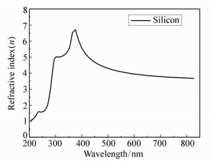
图 2 硅材料的折射率
Figure 2. Refractive index of silicon at wavelength ranging from 210~830 nm

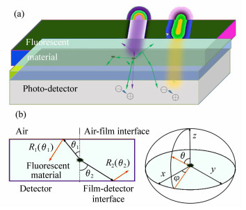
图 3 (a) 荧光转换紫外增强原理;(b)发光角度示意图
Figure 3. (a)Ultraviolet enhancement principle based on light conversion. (b)Schematic diagram to show light emission angle

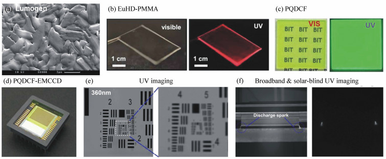
图 4 (a) PVD制备的Lumogen膜TEM图[49];(b)EuHD-PMMA膜在可见光和紫外光照射下的图像[58];(c)旋涂在石英基底上的钙钛矿量子点膜在日光和紫外光照射下的图像;(d)钙钛矿量子点薄膜增强的EMCCD;(e)360 nm紫外光成像(左),右图为中心区域的放大图像;(f)电晕放电宽光谱成像和日盲紫外成像
Figure 4. (a)SEM image of an Lumogen coating by PVD[49]; (b)Photographs of a quartz substrate coated with EuDH doped PMMA under ambient visible light and UV illuminations[58]; (c)Photographs of quartz substrate coated PQDCF under ambient daylight, and under a UV 365 nm lamp; (d)PQDCF coated EMCCD; (e)Digital output image of the EMCCD camera when the resolution test chart is illuminated by a 360 nm monochrome light. The right image is the enlarged central part of the left picture size in 100×100 pixels; (f)The broadband image of corona discharge equipment in operation, and the solar-blind UV image of the discharge spark

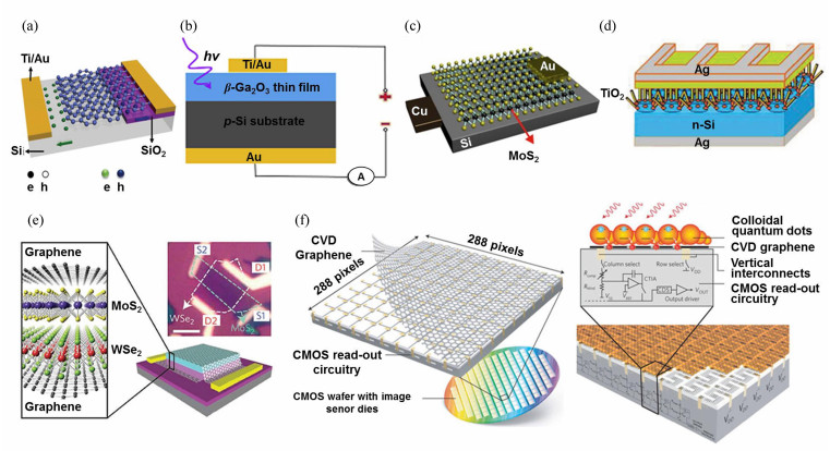
图 5 硅基低维材料探测器结构示意图。(a)硅基石墨烯探测器[76];(b)β-Ga2O3/p-Si异质结探测器[77];(c)MoS2/Si异质结探测器[79]; (d)TiO2纳米线/p-Si异质结探测器[80];(e)石墨烯MoS2/WSe2三明治结构光电器件[86];(f)硅基石墨烯/胶体量子点异质结388×288探测器阵列[87]
Figure 5. (a)Photodetector based on rGO/n-Si p-n vertical heterojunction[76]; (b)Schematic diagram of the fabricated b-Ga2O3/p-Si heterojunction structure[77]; (c)Schematic illustration of a MoS2/Si heterojunction device[79]; (d)Schematic illustration of a TiO2 nanorod arrays/n-Si heterojunction device[80]; (e)Schematic and optical image of MoS2/WSe2 junction sandwiched between top and bottom graphene electrodes[86]; (f)CMOS integration of CVD graphene with 388×288 pixel image sensor read-out circuit[87]

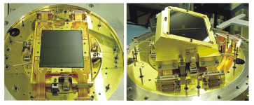
图 6 哈勃望远镜第三代广域照相机的背照射式紫外CCD探测器装配图
Figure 6. Assembly drawing of back-illuminated UV CCD detector for Hubble telescope third-generation camera

图 7 (a) 阿司匹林药物包衣均匀性分析,无包衣片剂(上)、包衣片剂(中)、包衣破损药物片剂(下)的可见图像(左)和365 nm紫外光照射下的吸收图像(右)[95];(b)降血糖药物盐酸二甲双胍(500 mg)在0.1 mL/mol盐酸溶液(含2 g/mL氯化钠和50 mM磷酸二氢钾)中的溶解过程,可见透射吸收图像(上),紫外透射吸收图像(下)[5]
Figure 7. (a)Image analysis of representative ASA tablets with either homogeneous or inhomogeneous coatings, photograhp and UV imaging of uncoated ASA tablet(top), coated ASA tablet(middle) and coated ASA tablet with coating defectes(bottom)[95]; (b)UV and visible absorbance maps obtained for Glucophage SR, 500 mg metformin HCl tablet in 0.1 M HCl containing 2.0 g/L NaCl and 50 mM KH2PO4[5]

图 8 紫外成像的电晕检测应用。(a)电晕探测仪器原理;(b)电晕放电图像:日盲图像(左上),可见图像(左下),融合图像(右);(c)太阳光谱与电晕放电光谱;(d)南非UViRCO公司的CoroCAM 8多光谱电晕成像仪;(e)以色列Ofil公司的Luminar手持紫外成像仪
Figure 8. Application of UV imaging in corona detection. (a)Schematic diagram of corona discharge detector; (b)Corona discharge image: solar blind image(upper left), visible image(lower left), fusion image(right); (c)Solar spectrum and corona discharge spectrum; (d)Multi-spectral corona imager CoroCAM 8 of UViRCO, South Africa; (e)Luminar hand held UV imager of Ofil, Israel

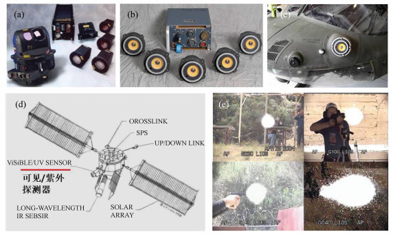
图 9 紫外成像的军事应用。(a)AN/AAR-54(V)紫外告警系统;(b)AN/AAR-57(V)紫外告警系统;(c)直升机上安装的AN/AAR-57(V);(d)美国太空跟踪与监视系统卫星示意图;(e)枪、炮口的可见紫外叠加图
Figure 9. Application of UV imaging in military. (a)The photograph of AN/AAR-54(V); (b)The photograph of AN/AAR-57(V); (c)AN/AAR-57(V) in helicopter; (d)The schematic of space tracking and surveillance system; (e)UV-visible fusion image of firing
表 1 硅基低维材料探测器的性能对比
Table 1. Comparison of the characteristic parameters of the photodetectors based on silicon and low dimension materials
探测器类型 波长/nm 光响应电流A/W 探测率(Jonmes) 响应时间 参考文献 rGO/n-Si 365~600 1.52 -- 0.002/0.0037 ms [76] β-Ga2O3/p-Si 254(solar-blind UV) 370 - 1.79 s [77] MoS2/Si 300~1 200 11.9 2.1×10¹⁰ 30.5/71.6 μs [78] MoS2/Si 250~1 200 23.1 1.63×10¹² 21.6/65.5 μs [79] TiO2/n-Si 300~600 0.3 - 18.5/19.1 ms [80] TiO2/p-Si 365~980 468 1.96×10¹⁴ 50/50 ms [81] ZnO/p-Si 365 101.2 - 0.44/0.59 s [82] Bi2Se3/Si 365~1 100 24.28 4.39×10¹² 2.5/5.5 μs [83] WS2/Si 370~1 064 0.7 2.7×10⁹ 4.1/4.4 s [84] In2Te3/Si 370~1 064 137 4.74×10¹⁰ 6/8 ms [85]  下载: 导出CSV
表 2 紫外增强硅基成像探测器的3种主要技术路线
Table 2. Three main technical routes for UV-enhanced silicon detectors
探测器类型 技术路线的特点 优点 缺点 发展方向 半导体工艺紫外增强CCD和CMOS 通过背照射、紫外窗口避免多晶、金属电极对紫外辐射的吸收,配合表面浅结处理增强器件紫外响应 面阵大、探测器内量子效率高、光谱响应宽 背照射和表面处理工艺复杂,成本高。紫外灵还敏需要特殊的增透处理,使可见和近红外波段效率降低 扩展EUV波段响应,发展高灵敏紫外EMCCD、sCMOS器件 荧光转换材料紫外增强硅探测器 利用荧光转换材料对紫外辐射吸收并发射与硅探测器工作光谱一致光子的特性,增强硅探测器紫外响应 工艺简单、成本低、面阵大、光谱响应宽 性能取决于荧光转换材料,EUV波段的光谱响应性能提升较少 发展光学性能好,荧光效率高的发光材料,突破荧光产率100%限制 低维材料硅基紫外探测器 在硅基底上制备低维材料,形成异质结突破硅材料带隙限制 单项性能指标优异,光谱响应超宽且可同窄波段日盲紫外响应 探测器外量子效率不高、以单元器件为主、综合性能偏低 发展多层高效率、高填充比面阵器件,优化材料制备和集成工艺
下载: 导出CSV
-
[1] MENDE S B, HEETDERKS H, FREY H U, et al.. Far ultraviolet imaging from the IMAGE spacecraft.2.wideband FUV imaging[J]. Space Science Reviews, 2000, 91(1-2):271-285. [2] LEITHERER C, VACCA W D, CONTI P S, et al.. Hubble space telescope ultraviolet imaging and spectroscopy of the bright starburst in the wolf-rayet galaxy NGC 4214[J]. Astrophysical Journal, 1996, 465(2):717-732. [3] HORINOUCHI T, KOUYAMA T, LEE Y J, et al.. Mean winds at the cloud top of Venus obtained from two-wavelength UV imaging by Akatsuki[J]. Earth Planets & Space, 2018, 70(1):10. [4] OKINO T, YAMAHIRA S, YAMADA S, et al.. A real-time ultraviolet radiation imaging system using an organic photoconductive image sensor[J]. Sensors, 2018, 18(1), doi: 10.3390/S1B010314. [5] STERGAARD J. UV imaging in pharmaceutical analysis[J]. Journal of Pharmaceutical & Biomedical Analysis, 2018, 147:140. [6] NOVIKOVA A, CARSTENSEN J M, ZEITLER J A, et al.. Multispectral UV imaging for determination of the tablet coating thickness[J]. Journal of Pharmaceutical Sciences, 2017, 106(6):1560-1569. doi: 10.1016/j.xphs.2017.02.016 [7] 周峰, 郑国宪, 闫锋, 等.天基紫外预警技术发展现状及思考[J].航天返回与遥感, 2012, 33(6):39-44. http://d.old.wanfangdata.com.cn/Periodical/htfhyyg201206007ZHOU F, ZHENG G X, YAN F, et al.. Development status and thoughts of space-based UV warning technology[J]. Spacecraft Recovery & Remote Sensing, 2012, 33(6):39-44.(in Chinese) http://d.old.wanfangdata.com.cn/Periodical/htfhyyg201206007 [8] DING J, LI X, ZHU X, et al.. Solar-irradiated leakage of UV camera for daytime corona inspection[C]. Electrical Insulation and Dielectric Phenomena, 2015: 298-301. [9] MCCLINTOCK W E, RUSCH D W, THOMAS G E, et al.. The cloud imaging and particle size experiment on the Aeronomy of ice in the mesosphere mission:instrument concept, design, calibration, and on-orbit performance[J]. Journal of Atmospheric and Solar-Terrestrial Physics, 2009, 71(3-4):340-355. doi: 10.1016/j.jastp.2008.10.011 [10] 毛小洁.高功率皮秒紫外激光器新进展[J].中国光学, 2015, 8(2):182-190. http://www.chineseoptics.net.cn/CN/abstract/abstract9255.shtmlMAO X J. New progress in high-power picosecond ultraviolet laser[J]. Chinese Optics, 2015, 8(2):182-190.(in Chinese) http://www.chineseoptics.net.cn/CN/abstract/abstract9255.shtml [11] 周影, 娄洪伟, 周跃, 等.微弱日盲紫外电晕自动实时检测方法[J].中国光学, 2015, 8(6):926-932. http://www.chineseoptics.net.cn/CN/abstract/abstract9364.shtmlZHOU Y, LOU H W, ZHOU Y, et al.. Automatic real-time detection method of faint solar-blind ultraviolet corona[J]. Chinese Optics, 2015, 8(6):926-932. http://www.chineseoptics.net.cn/CN/abstract/abstract9364.shtml [12] 程宏昌, 端木庆铎, 石峰, 等.双微通道板紫外像增强器工作特性研究[J].真空科学与技术学报, 2013, 33(6):524-527. doi: 10.3969/j.issn.1672-7126.2013.06.04CHENG H CH, DUANMU Q Z, SHI F, et al.. Characterization of solar blind double micro-channel plate ultraviolet image intensifier[J]. Chinese Journal of Vacuum Science & Technology, 2013, 33(6):524-527.(in Chinese) doi: 10.3969/j.issn.1672-7126.2013.06.04 [13] 黄钧良.MAMA紫外探测器系统与高增益MCP[J].红外技术, 1997(4):33-35. doi: 10.1038-nm0710-731a/HUANG J L. Evaluation of MAMA ultraviolet detectors and their applications[J]. Infrared Technology, 1997(4):33-35.(in Chinese) doi: 10.1038-nm0710-731a/ [14] YOSHIKAWA I. Ultraviolet detector with CMOS-coupled microchannel plates for future space missions[C]. Space Telescopes and Instrumentation 2016: Ultraviolet to Gamma Ray, 2016: 9905: 99053G. [15] JOSEPH C L, WOODGATE B E. UV imaging detectors:high-QE EBCMOS enabling new science missions[J]. American Astronomical Society, 2011, 43 [16] 尼启良.使用曲面微通道板和感应电荷位置灵敏阳极的软X射线-极紫外光子计数成像探测器研究[J].中国光学, 2015, 8(5):847-872. http://www.chineseoptics.net.cn/CN/abstract/abstract9354.shtmlNI Q L. Soft X-ray and extreme ultraviolet photon-counting imaging detector with curved surface micro-channel plate and induced charge position-sensitive anode[J]. Chinese Optics, 2015, 8(5):847-872.(in Chinese) http://www.chineseoptics.net.cn/CN/abstract/abstract9354.shtml [17] 卜绍芳, 尼启良, 何玲平, 等.极紫外波段微通道板光子计数探测器[J].中国光学, 2012, 5(3):302-309. doi: 10.3969/j.issn.2095-1531.2012.03.019BU SH F, NI Q L, HE L P, et al.. Microchannel plate photon counting detector in UV range[J]. Chinese Optics, 2012, 5(3):302-309.(in Chinese) doi: 10.3969/j.issn.2095-1531.2012.03.019 [18] MONROY E, OMN S F, CALLE F. Topical review:wide-bandgap semiconductor ultraviolet photodetectors[J]. Semiconductor Science & Technology, 2003, 18(4):R33. [19] ALAIE Z, NEJAD S M, YOUSEFI M H. Recent advances in ultraviolet photodetectors[J]. Materials Science in Semiconductor Processing, 2015, 29:16-55. doi: 10.1016/j.mssp.2014.02.054 [20] GAMBINI S, SKUCHA K, LIU P, et al.. A CMOS 10kpixel baseline-free magnetic bead detector with column-parallel readout for miniaturized immunoassays[C]. Solid-State Circuits Conference Digest of Technical Papers, 2012: 126-128. [21] MA B, SHANG Z, HU Y, et al.. Atmospheric seeing measurement from bright star trails with frame transfer CCDs[C]. SPIE Astronomical Telescopes & Instrumentation, 2016: 99060A. [22] MA B, WANG L, BOGGS K, et al.. The test of the 10k×10k CCD for Antarctic Survey Telescopes(AST3)[J]. Ground-based and Airborne Instrumentation for Astronomy IV.Proceedings of the SPIE, 2012, 8446(8446):572-577. [23] NIKZAD S, HOENK M, JEWELL A D, et al.. Single photon counting uv solar-blind detectors using silicon and Ⅲ-nitride materials[J]. Sensors, 2016, 16(6):927. doi: 10.3390/s16060927 [24] PALIK E D. Handbook of Optical Constants of Solids Ⅱ[M]. Academic Press, 1985. [25] ASPNES D E, STUDNA A A. Dielectric functions and optical parameters of Si, Ge, GaP, GaAs, GaSb, InP, InAs, and InSb from 1.5 to 6.0 eV[J]. Physical Review B, 1983, 27(2):985-1009. doi: 10.1103/PhysRevB.27.985 [26] TALMI Y, SIMPSON R W. Self-scanned photodiode array:a multichannel spectrometric detector[J]. Applied Optics, 1980, 19(9):1401-1414. doi: 10.1364/AO.19.001401 [27] VOGT S S, TULL R G, KELTON P. Self-scanned photodiode array:high performance operation in high dispersion astronomical spectrophotometry[J]. Applied Optics, 1978, 17(4):574-592. doi: 10.1364/AO.17.000574 [28] STERN R A, CATURA R C, KIMBLE R, et al.. Ultraviolet and extreme ultraviolet response of charge-coupled-device detectors[J]. Optical Engineering, 1987, 26(9):875-883. [29] MASAHARU M, HIROSHI A, KATSUMI S, et al.. Greater-than-90% QE in visible spectrum perceptible from UV to near-IR Hamamatsu thinned back-illuminated CCDs[J]. Solid State Sensor Arrays:Development and Applications, 1997:2-9. [30] HOENK M E, GRUNTHANER P J, GRUNTHANER F J, et al.. Growth of a delta-doped silicon layer by molecular beam epitaxy on a charge-coupled device for reflection-limited ultraviolet quantum efficiency[J]. Applied Physics Letters, 1992, 61(9):1084-1086. doi: 10.1063/1.107675 [31] BLACKSBERG J, NIKZAD S, HOENK M E, et al.. Near-100% quantum efficiency of delta doped large-format UV-NIR silicon imagers[J]. IEEE Transactions on Electron Devices, 2008, 55(12):3402-3406. doi: 10.1109/TED.2008.2006779 [32] HYNECEK J. CCM-a new low-noise charge carrier multiplier suitable for detection of charge in small pixel CCD image sensors[J]. IEEE Transactions on Electron Devices, 1992, 39(8):1972-1975. doi: 10.1109/16.144694 [33] JACQUOT B, MARTIN C, SCHIMINOVICH D, et al.. Delta-doped electron-multiplied CCD with absolute quantum efficiency over 50% in the near to far ultraviolet range for single photon counting applications[J]. Applied Optics, 2012, 51(3):365-369. doi: 10.1364/AO.51.000365 [34] PRYDDERCH M L, WALTHAM N R, MORRISSEY Q, et al.. A large-area CMOS monolithic active pixel sensor for extreme ultraviolet spectroscopy and imaging[J]. Proc SPIE, 2004, 5301:175-185. doi: 10.1117/12.526401 [35] WALTHAM N R, PRYDDERCH M, MAPSON-MENARD H, et al.. Development of a thinned back-illuminated CMOS active pixel sensor for extreme ultraviolet spectroscopy and imaging in space science[J]. Nuclear Instruments & Methods in Physics Research, 2007, 573(1-2):250-252. [36] HALAIN J P, MAZZOLI A, ROCHUS P, et al.. EUV high resolution imager on-board sOLAR oRBITer: optical design and detector performances[C]. International Conference on Space Optics ICSO2012, 2012, 10564: 105643V. [37] HALAIN J P, HERMANS L, MEYNANTS G. The dual-gain 10μm back-thinned 3k×3k CMOS-APS detector of the solar orbiter extreme UV imager[J]. Proceedings of SPIE-The International Society for Optical Engineering, 2014, 9144:914431. [38] KURODA R, KAWADA S, NASUNO S, et al.. A CMOS image sensor with 200-1000 nm spectral response and high robustness to ultraviolet light exposure[J]. ITE Technical Report, 2013, 37:21-24. [39] NASUNO S, WAKASHIMA S, KUSUHARA F, et al.. A CMOS image sensor with 240μV/e-conversion gain, 200 ke-full well capacity, 190-1000 nm spectral response and high robustness to UV light[J]. ITE Transactions on Media Technology and Applications, 2016, 4(2):116-122. doi: 10.3169/mta.4.116 [40] HOENK M E, JONES T J, DICKIE M R, et al.. Delta-doped back-illuminated CMOS imaging arrays:progress and prospects[J]. Proceedings of SPIE-The International Society for Optical Engineering, 2009, 7419:74190T. http://d.old.wanfangdata.com.cn/NSTLHY/NSTL_HYCC0210142577/ [41] HAMDEN E T, GREER F, HOENK M E, et al.. Ultraviolet antireflection coatings for use in silicon detector design[J]. Applied Optics, 2011, 50(21):4180-4188. doi: 10.1364/AO.50.004180 [42] HAMDEN E T, JEWELL A D, SHAPIRO C A, et al.. Charge-coupled devices detectors with high quantum efficiency at UV wavelengths[J]. Journal of Astronomical Telescopes Instruments & Systems, 2016, 2(3):036003. [43] BLOUKE M M, COWENS M W, HALL J E, et al.. A UV sensitive CCD detector[C]. Electron Devices Meeting, 1979 Internationa, 1979: 141-143. [44] BLOUKE M M, COWENS M W, HALL J E, et al.. Ultraviolet downconverting phosphor for use with silicon CCD imagers[J]. Applied Optics, 1980, 19(19):3318-3321. doi: 10.1364/AO.19.003318 [45] COWENS M W, BLOUKE M M, FAIRCHILD T, et al.. Coronene and liumogen as VUV sensitive coatings for Si CCD imagers:a comparison[J]. Applied Optics, 1980, 19(22):3727-3728. doi: 10.1364/AO.19.003727 [46] VIEHMANN A W, BUTNER C L, COWENS M W. Ultraviolet/UV/sensitive phosphors for silicon imaging detectors[J]. Proceedings of SPIE-The International Society for Optical Engineering, 1981, 279(12):146-152. [47] MORRISSEY P F, MCCANDLISS S R, FELDMAN P D, et al. Ultraviolet performance of a lumigen-coated CCD[J]. Bulletin of the American Astronomical Society, 1991, 23:1316. [48] DAMENTO M A, BARCELLOS A A, SCHEMPP W V. Stability of lumogen films on CCDs[C]. IS&T/SPIE's Symposium on Electronic Imaging: Science & Technology, 1995: 204-210. [49] DESLANDES A, WEDDING A B, CLARKE S R, et al.. Characterization of PVD Lumogen films for wavelength conversion applications[C]. Smart Materials, Nano-, and Micro-Smart Systems, 2005: 616-626. [50] 张大伟, 田鑫, 黄元申, 等.CCD紫外敏感Lumogen薄膜制备与光谱表征[J].光谱学与光谱分析, 2010, 30(5):1171-1174. doi: 10.3964/j.issn.1000-0593(2010)05-1171-04ZHANG D W, TIAN X, HUANG Y SH, et al.. Preparation and spectral characterization of Lumogen coatings for UV-responsive CCD image sensors[J]. Spectroscopy & Spectral Analysis, 2010, 30(5):1171-1174.(in Chinese) doi: 10.3964/j.issn.1000-0593(2010)05-1171-04 [51] 杜晨光, 孙利群, 丁志田.利用晕苯增强CCD紫外响应的实验研究[J].光学技术, 2010, 36(5):753-757. http://d.old.wanfangdata.com.cn/Periodical/gxjs201005025DU CH G, SUN L Q, DING ZH T. Experiment study of enhancing CCD ultraviolet response using coronene[J]. Optical Technique, 2010, 36(5):753-757.(in Chinese) http://d.old.wanfangdata.com.cn/Periodical/gxjs201005025 [52] 何梁, 张大伟, 陶春先, 等.旋涂法和热蒸发制备紫外CCD用晕苯薄膜的性能对比[J].光谱学与光谱分析, 2014, 34(5):1319-1322. doi: 10.3964/j.issn.1000-0593(2014)05-1319-04HE L, ZHANG D W, TAO CH X, et al.. Performance comparison of coronene film for UV-CCD prepared by spin-coating and physical vapor deposition[J]. Spectroscopy & Spectral Analysis, 2014, 34(5):1319-1322.(in Chinese) doi: 10.3964/j.issn.1000-0593(2014)05-1319-04 [53] 姜霖, 张大伟, 陶春先, 等.紫外增强Lumogen薄膜旋涂法制备及其性能表征[J].光谱学与光谱分析, 2013, 33(2):468-470. doi: 10.3964/j.issn.1000-0593(2013)02-0468-03JIANG L, ZANG D W, TAO CH X, et al. Preparation by spin-coating technology and characterization of UV-enhanced Lumogen film[J]. Spectroscopy & Spectral Analysis, 2013, 33(2):468-470.(in Chinese) doi: 10.3964/j.issn.1000-0593(2013)02-0468-03 [54] 冯宇祥, 孟银霞, 张国玉, 等.CCD紫外增强薄膜旋涂法工艺优化[J].光谱学与光谱分析, 2017, 37(9):2826-2831. http://d.old.wanfangdata.com.cn/Periodical/gpxygpfx201709031FENG Y X, MENG Y X, ZHANG G Y, et al.. Process optimization of CCD UV-responsive sensitivity enhancement by spin-coating[J]. Spectroscopy & Spectral Analysis, 2017, 37(9):2826-2831.(in Chinese) http://d.old.wanfangdata.com.cn/Periodical/gpxygpfx201709031 [55] 刘琼, 马守宝, 钱晓晨, 等.CMOS传感器紫外敏化膜层的厚度优化及其光电性能测试[J].光子学报, 2017, 46(6):225-230. http://d.old.wanfangdata.com.cn/Periodical/gzxb201706031LIU Q, MA SH B, QIAN X CH, et al.. Thickness optimization and photoelectric performance test of UV sensitized film of CMOS sensor[J]. Acta Photonica Sinica, 2017, 46(6):225-230.(in Chinese) http://d.old.wanfangdata.com.cn/Periodical/gzxb201706031 [56] FRANKS W A R, KⅡK M J, NATHAN A. UV-responsive CCD image sensors with enhanced inorganic phosphor coatings[J]. IEEE Transactions on Electron Devices, 2003, 50(2):352-358. doi: 10.1109/TED.2003.809029 [57] 刘猛, 张大伟, 谢品, 等.增强光电图像传感器紫外探测薄膜的制备[J].仪表技术与传感器, 2009, 30(9):12-14. doi: 10.3969/j.issn.1002-1841.2009.09.005LIU M, ZHANG D W, XIE P, et al.. Investigation in UV-enhanced coatings based on Zn2SiO4:Mn for image sensors[J]. Instrument Technique & Sensor, 2009, 30(9):12-14.(in Chinese) doi: 10.3969/j.issn.1002-1841.2009.09.005 [58] SHENG X, YU C, MALYARCHUK V, et al.. Photodetectors:silicon-based visible-blind ultraviolet detection and imaging using down-shifting luminophores[J]. Advanced Optical Materials, 2014, 2(4):314-319. doi: 10.1002/adom.v2.4 [59] TAI Y, LI X, PAN B. Efficient near-infrared down conversion in Nd3+-Yb3+ co-doped transparent nanostructured glass ceramics for photovoltaic application[J]. Journal of Luminescence, 2018, 195:102-108. doi: 10.1016/j.jlumin.2017.10.051 [60] SONG Y, YOU H, HUANG Y, et al.. Highly uniform and monodisperse Gd(2)O(2)S:Ln(3+)(Ln=Eu, Tb) submicrospheres:solvothermal synthesis and luminescence properties[J]. Inorganic Chemistry, 2010, 49(24):11499-11504. doi: 10.1021/ic101608b [61] STRMPEL C, MCCANN M, BEAUCARNE G, et al.. Modifying the solar spectrum to enhance silicon solar cell efficiency-an overview of available materials[J]. Solar Energy Materials & Solar Cells, 2007, 91(4):238-249. [62] ARQUER FPGD, ARMIN A, MEREDITH P, et al. Corrigendum:solution-processed semiconductors for next-generation photodetectors[J]. Nature Reviews Materials, 2017, 2(3):16100. doi: 10.1038/natrevmats.2016.100 [63] HAN H V, LU A Y, LU L S, et al.. Photoluminescence enhancement and structure repairing of monolayer MoSe2 by hydrohalic acid treatment[J]. Acs Nano, 2016, 10(1):1454-1461. doi: 10.1021/acsnano.5b06960 [64] KAGAN C R, LIFSHITZ E, SARGENT E H, et al.. Building devices from colloidal quantum dots[J]. Science, 2016, 353(6302):885. http://d.old.wanfangdata.com.cn/NSTLQK/NSTL_QKJJ0227499384/ [65] GEYER S M, SCHERER J M, MOLOTO N, et al.. Efficient luminescent down-shifting detectors based on colloidal quantum dots for dual-band detection applications[J]. Acs Nano, 2011, 5(7):5566-5571. doi: 10.1021/nn2010238 [66] JIANG L, SUN H, XU B, et al.. The spectrum of quantum dots film for UV CCD[J]. Journal of Spectroscopy, 2013:1-5. [67] BHASKARAN S. First report on quantum dot coated CMOS CID arrays for the UV and VUV[J]. Proceedings of SPIE-The International Society for Optical Engineering, 2013, 8859(10):1877-1889. [68] KOVALENKO M V, PROTESESCU L, BODNARCHUK M I. Properties and potential optoelectronic applications of lead halide perovskite nanocrystals[J]. Science, 2017, 358(6364):745-750. doi: 10.1126/science.aam7093 [69] ZHOU Q C, BAI Z L, LU W G, et al.. In situ fabrication of halide perovskite nanocrystal-embedded polymer composite films with enhanced photoluminescence for display backlights[J]. Advanced Materials, 2016, 28(41):9163-9168. doi: 10.1002/adma.201602651 [70] ZHANG M, WANG L, MENG L, et al.. Perovskite quantum dots embedded composite films enhancing UV response of silicon photodetectors for broadband and solar-blind light detection[J]. Advanced Optical Materials, 2018:1800077. [71] LIU Y, WEISS NO, DUAN X, et al.. Van der Waals heterostructures and devices[J]. Nature Reviews Materials, 2016, 1(9):16042. doi: 10.1038/natrevmats.2016.42 [72] CHHOWALLA M, JENA D, ZHANG H. Two-dimensional semiconductors for transistors[J]. Nature Reviews Materials, 2016, 1(11):16052. doi: 10.1038/natrevmats.2016.52 [73] SUN Z, MARTINEZ A, WANG F. Optical modulators with 2D layered materials[J]. Nature Photonics, 2016, 10(4):227-238. doi: 10.1038/nphoton.2016.15 [74] ELKADY M F, SHAO Y, KANER R B. Graphene for batteries, supercapacitors and beyond[J]. Nature Reviews Materials, 2016, 1(7):16033. doi: 10.1038/natrevmats.2016.33 [75] WANG Y M, DING K, SUN B Q, et al.. Two-dimensional layered material/silicon heterojunctions for energy and optoelectronic applications[J]. Nano Research, 2016, 9(1):72-93. doi: 10.1007/s12274-016-1003-3 [76] LI G, LIU L, WU G, et al.. Self-powered UV-near infrared photodetector based on reduced graphene oxide/n-Si vertical heterojunction[J]. Small, 2016, 12(36):5019-5026. doi: 10.1002/smll.201600835 [77] GUO X C, HAO N H, GUO D Y, et al.. β -Ga2O3/p-Si heterojunction solar-blind ultraviolet photodetector with enhanced photoelectric responsivity[J]. Journal of Alloys & Compounds, 2016, 660:136-140. [78] ZHANG Y, YU Y, MI L, et al.. In situ fabrication of vertical multilayered MoS2/Si homotype heterojunction for high-speed visible-near-infrared photodetectors[J]. Small, 2016, 12(8):1062-1071. doi: 10.1002/smll.201502923 [79] LOU Z, ZENG L, WANG Y, et al.. High-performance MoS2/Si heterojunction broadband photodetectors from deep ultraviolet to near infrared[J]. Optics Letters, 2017, 42(17):3335-3338. doi: 10.1364/OL.42.003335 [80] JI T, LIU Q, ZOU R, et al.. An interface engineered multicolor photodetector based on n-Si(111)/TiO2 nanorod array heterojunction[J]. Advanced Functional Materials, 2016, 26(9):1400-1410. doi: 10.1002/adfm.201504464 [81] LING C C, GUO T C, LU W B, et al. Ultrahigh photosensitivity and detectivity of hydrogen-treated TiO2 nanorod array/SiO2/Si heterojunction broadband photodetectors and its mechanism[J]. Journal of Materials Chemistry C, 2018, 6(9):2319-2328. doi: 10.1039/C7TC05580C [82] FLEMBAN T H, HAQUE M A, AJIA I A, et al.. A photodetector based on p-Si/n-ZnO nanotube heterojunctions with high ultraviolet responsivity[J]. Acs Applied Materials & Interfaces, 2017, 9(42):37120-37127. [83] ZHANG H, ZHANG X, LIU C, et al.. High-responsivity, high-detectivity, ultrafast topological insulator Bi2Se3/silicon heterostructure broadband photodetectors[J]. Acs Nano, 2016, 10(5):5113-5122. doi: 10.1021/acsnano.6b00272 [84] YAO J D, ZHENG Z Q, SHAO J M, et al.. Stable, highly-responsive and broadband photodetection based on large-area multilayered WS2 films grown by pulsed-laser deposition[J]. Nanoscale, 2015, 7(36):14974-14981. doi: 10.1039/C5NR03361F [85] YAO J, SHAO J, WANG Y, et al.. Ultra-broadband and high response of the Bi2Te3-Si heterojunction and its application as a photodetector at room temperature in harsh working environments[J]. Nanoscale, 2015, 7(29):12535-12541. doi: 10.1039/C5NR02953H [86] LEE GH, CUI X, KIM P. Atomically thin p-n junctions with van der Waals heterointerfaces[J]. Nature Nanotechnology, 2014, 9(9):676-681. doi: 10.1038/nnano.2014.150 [87] GOOSSENS S, NAVICKAITE G, MONASTERIO C, et al.. Broadband image sensor array based on graphene CMOS integration[J]. Nature Photonics, 2017, 11(6):366-371. doi: 10.1038/nphoton.2017.75 [88] 阮宁娟, 苏云.国外紫外空间探测器发展综述[J].航天返回与遥感, 2008, 29(3):71-78. doi: 10.3969/j.issn.1009-8518.2008.03.013RUAN N J, SU Y. Summarization of overseas space ultraviolet instrument development[J]. Spacecraft Recovery & Remote Sensing, 2008, 29(3):71-78.(in Chinese) doi: 10.3969/j.issn.1009-8518.2008.03.013 [89] 张燕, 龚海梅, 白云, 等.空间用紫外探测及AlGaN探测器的研究进展[J].激光与红外, 2006, 36(11):1009-1012. doi: 10.3969/j.issn.1001-5078.2006.11.001ZHANG Y, GONG H M, BAI Y, et al. UV detection applied to space and the research development of AlGaN detector[J]. Laser & Infrared, 2006, 36(11):1009-1012.(in Chinese) doi: 10.3969/j.issn.1001-5078.2006.11.001 [90] GLADSTONE G R, PERSYN S C, ETERNO J S, et al.. The ultraviolet spectrograph on NASA's Juno mission[J]. Space Science Reviews, 2017, 213:1-27. doi: 10.1007/s11214-017-0430-0 [91] MENDE S B, FREY H U, RIDER K, et al. The far ultraviolet imager on the icon mission[J]. Space Science Reviews, 2017, 212:1-42. doi: 10.1007/s11214-016-0319-3 [92] MCMASTER M, AL E. Wide Field and Planetary Camera 2 Instrument Handbook v. 10.0[M]. Wide Field & Planetary Camera Hst Instrument Handbook, 2008. [93] DRESSEL L. Wide Field Camera 3 Instrument Handbook for Cycle 21 v. 5.0[M]. Wide Field Camera 3, HST Instrument Handbook, 2012. [94] KHAN A R, CHORDIA P, GANDORFER A M. The solar ultraviolet imaging telescope onboard aditya-L1[C]. SPIE Astronomical Telescopes and Instrumentation, 2016: 990504. [95] KLUKKERT M, WU J X, RANTANEN J, et al.. Rapid assessment of tablet film coating quality by multispectral UV imaging[J]. Aaps Pharmscitech, 2016, 17(4):958-967. doi: 10.1208/s12249-015-0414-x [96] 石峰, 程宏昌, 闫磊, 等.紫外探测技术[M].北京:国防工业出版社, 2017.SHI F, CHENG H CH, YAN L. UV Detection Tchnique[M]. Beijing:National Defense Industry Press, 2017.(in Chinese) [97] PRATT H, HASSANIN K, TROUGHTON L D, et al.. UV imaging reveals facial areas that are prone to skin cancer are disproportionately missed during sunscreen application[J]. Plos One, 2017, 12(10):e0185297. doi: 10.1371/journal.pone.0185297 [98] LI Y, WANG T, GUO L, et al.. Detection and analysis of high voltage electrical equipment corona discharge based on ultraviolet imaging technology[C]. Control and Decision Conference, 2017: 6928-6931. [99] 叶柏松, 袁永刚, 王继强, 等.一种便携式电晕检测紫外相机的设计[J].红外, 2013, 34(4):24-27. doi: 10.3969/j.issn.1672-8785.2013.04.005YE B S, YUAN Y G, WANG J Q, et al.. Design of a portable UV camera for corona detection[J]. Infrared, 2013, 34(4):24-27.(in Chinese) doi: 10.3969/j.issn.1672-8785.2013.04.005 [100] 刘建卓, 王学进, 黄剑波, 等.三波段电晕检测光学系统的设计[J].光学精密工程, 2011, 19(6):1228-1234. http://d.old.wanfangdata.com.cn/Periodical/gxjmgc201106008LIU J ZH, WANG X J, HUANG J B, et al.. Design of three-band optical system used in corona detection[J]. Opt. Precision Eng., 2011, 19(6):1228-1234.(in Chinese) http://d.old.wanfangdata.com.cn/Periodical/gxjmgc201106008 [101] 张洁.机载导弹逼近告警技术发展分析[J].舰船电子工程, 2014, 34(11):19-23. http://d.old.wanfangdata.com.cn/Periodical/jcdzgc201411006ZHANG J. Development and analysis of airborne missile warning technology[J]. Ship Electronic Engineering, 2014, 34(11):19-23.(in Chinese) http://d.old.wanfangdata.com.cn/Periodical/jcdzgc201411006 [102] THOMPSON N J, WILSON M W, CONGREVE D N, et al.. Energy harvesting of non-emissive triplet excitons in tetracene by emissive PbS nanocrystals[J]. Nature Materials, 2014, 13(11):1039-1043. doi: 10.1038/nmat4097 [103] SONI A, PUROHIT S, HEGDE R S. Multilayered aluminum plasmonic metasurfaces for ultraviolet bandpass filtering[J]. IEEE Photonics Technology Letters, 2017, 29(1):110-113. doi: 10.1109/LPT.2016.2629504 [104] MACKENTY J W. A near ultraviolet solar-blind telescope design using silicon CCD detectors[C]. Space Telescopes and Instrumentation 2016: Ultraviolet to Gamma Ray, 2016: 990538. [105] LI W D, CHOU S Y. Solar-blind deep-UV band-pass filter(250-350 nm) consisting of a metal nano-grid fabricated by nanoimprint lithography[J]. Optics Express, 2010, 18(2):931-937. doi: 10.1364/OE.18.000931 -

 下载:
下载:


计量
- 文章访问数: 6881
- HTML全文浏览量: 2725
- PDF下载量: 642
- 被引次数: 0
