


-
摘要: 传统的CMOS图像传感器一般采用基于LV-CMOS工艺的N阱/P型衬底制备的PN光电二极管或者PPD二极管作为光敏元。PIN光敏元具有结电容小、量子效率高的特点。采用HV-CMOS(高压CMOS)工艺可以实现CMOS电路与PIN光敏元的单片集成。本文研究了集成PIN光敏元的CMOS探测器的光电响应特性以及NEP随像素大小和复位电压的变化关系。研究表明,将光敏元从PN光电二极管改为PIN光电二极管后,像素电荷增益可以提高一个数量级左右;同时,像素的瞬态电荷增益要大于传统认为的1/Cpd,并与二极管的大小以及复位电压紧密相关。研究发现,小像素因其更高的电荷增益和更低的等效噪声,更加适合弱信号下的短积分时间快速探测。若配合微透镜的使用,小像素在微光探测方面可以获得更大的优势。Abstract: Traditional CMOS image sensors generally use PN photodiodes or PPDs as the photosensitive element, which are formed based on N-well/P-type substrates using the LV-CMOS process. The PIN photosensitive element has small junction capacitance and high quantum efficiency. By using High-Voltage CMOS(HV-CMOS), monolithic integration of CMOS circuits with PIN photodiodes can be achieved. In this paper, the relationship between the photo-response characteristics, NEP of CMOS detectors and pixel size and reset voltage are studied. The results show that the pixel charge gain can be increased by about one order of magnitude when the photosensitive element is changed from PN to PIN and the transient charge gain of the pixel is larger than 1/Cpd. This is closely related to the size of the diode and reset voltage. It is found that small pixels are more suitable for fast detection of short integration time under weak signals because of their higher charge gain and lower equivalent noise. If combined with microlenses, small pixels can be further advantageous in low light detection.
-
Key words:
- CMOS image sensor /
- HV-CMOS /
- PIN photodiodes /
- 3T pixel structure
-
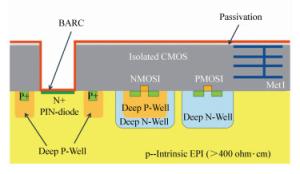
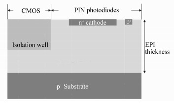
图 2 PIN光敏元与CMOS电路单片集成
Figure 2. Monolithic integration of PIN photosensitive element and CMOS circuit
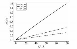
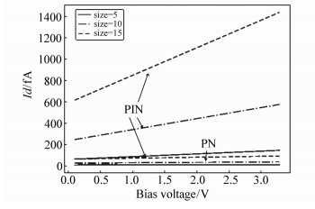
图 11 光信号电压变化与光电流关系
Figure 11. Relationship between photo signal voltage variation and photo current

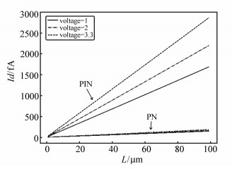
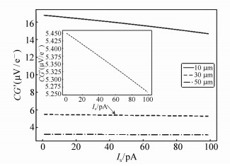
图 12 瞬态电荷转换增益随光电流变化关系
Figure 12. Relationship between transient charge conversion gain and photo current variance
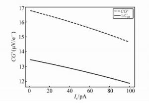
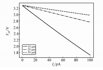
图 13 瞬态电荷增益与电容值倒数的比较
Figure 13. Comparison between transient charge gain and the reciprocal of capacitance value
表 1 公式参数
Table 1. Formula parameters
Parameter PN photodiode(LV-CMOS) PIN photodiode(HV-CMOS) Area junction capacitance for zero bias:CJ 97 pF/mm2 0.93 pF/mm2 Area capacitance grading coefficient:MJ 0.31 0.05 Area capacitance junction potentials:PB 0.42 V 0.31 V Perimeter junction capacitance for zero bias:CJSW 0.52 pF/mm 0.35 pF/mm Perimeter capacitance grading coefficient:MJSW 0.21 0.21 Perimeter capacitance junction potentials:PBSW 0.38 V 0.16 V Area leakage current density:JS 1.27 pA/mm2 2.07 pA/mm2 Perimeter leakage current density:JSSW 28.8 fA/mm 2.91 pA/mm Voltage dependent area leakage conductivity:GLEAK 0 pA/V/mm2 0 pA/V/mm2 Voltage dependent perimeter leakage conductivity:GLEAKSW 44 fA/V/mm 1.29 pA/V/mm  下载: 导出CSV
-
[1] 何家维, 何昕, 魏仲慧, 等.高灵敏度EMCCD导航相机的设计[J].光学 精密工程, 2018, 26(12):3019-3027. http://d.old.wanfangdata.com.cn/Periodical/gxjmgc201812019HE J W, HE X, WEI ZH H, et al.. Design of high-sensitivity EMCCD navigation camera[J]. Opt. Precision Eng., 2018, 26(12):3019-3027.(in Chinese) http://d.old.wanfangdata.com.cn/Periodical/gxjmgc201812019 [2] 何伟基, 司马博羽, 程耀进, 等.基于盖格-雪崩光电二极管的光子计数成像[J].光学 精密工程, 2012, 20(8):1831-1837. http://d.old.wanfangdata.com.cn/Periodical/gxjmgc201208025HE W J, SIMA B Y, CHENG Y J, et al.. Photon counting imaging based on GM-APD[J]. Opt. Precision Eng., 2012, 20(8):1831-1837.(in Chinese) http://d.old.wanfangdata.com.cn/Periodical/gxjmgc201208025 [3] 刘超, 张晓晖.超低照度下微光图像的深度卷积自编码网络复原[J].光学 精密工程, 2018, 26(4):951-961. http://d.old.wanfangdata.com.cn/Periodical/gxjmgc201804025LIU CH, ZHANG X H. Deep convolutional autoencoder networks approach to low-light level image restoration under extreme low-light illumination[J]. Opt. Precision Eng., 2018, 26(4):951-961.(in Chinese) http://d.old.wanfangdata.com.cn/Periodical/gxjmgc201804025 [4] 陈莹, 朱明, 刘剑, 等.高斯混合模型自适应微光图像增强[J].液晶与显示, 2015, 30(2):300-309. http://d.old.wanfangdata.com.cn/Periodical/yjyxs201502019CHEN Y, ZHU M, LIU J, et al.. Automatic low light level image enhancement using Gaussian mixture modeling[J]. Chinese Journal of Liquid Crystals and Displays, 2015, 30(2):300-309.(in Chinese) http://d.old.wanfangdata.com.cn/Periodical/yjyxs201502019 [5] 王田珲, 李豫东, 文林, 等.CMOS图像传感器在质子辐照下热像素的产生和变化规律[J].发光学报, 2018, 39(12):1697-1704. http://d.old.wanfangdata.com.cn/Periodical/fgxb201812008WANG T H, LI Y D, WEN L, et al.. Generation and annealing of hot pixels of CMOS image sensor induced by proton[J]. Chinese Journal of Luminescence, 2018, 39(12):1697-1704.(in Chinese) http://d.old.wanfangdata.com.cn/Periodical/fgxb201812008 [6] 玛丽娅, 李豫东, 郭旗, 等.CMOS有源像素图像传感器的电子辐照损伤效应研究[J].发光学报, 2017, 38(2):182-187. http://d.old.wanfangdata.com.cn/Periodical/fgxb201702009MA L Y, LI Y D, GUO Q, et al.. Electron beam radiation effects on CMOS active pixel sensor[J]. Chinese Journal of Luminescence, 2017, 38(2):182-187.(in Chinese) http://d.old.wanfangdata.com.cn/Periodical/fgxb201702009 [7] 徐守龙, 邹树梁, 黄有骏, 等.CCD与CMOS像素传感器γ射线电离辐射响应特性对比研究[J].发光学报, 2018, 39(6):815-822. http://d.old.wanfangdata.com.cn/Periodical/fgxb201806010XU SH L, ZOU SH L, HUANG Y J, et al.. Comparative study on γ-ray radiation response characteristics of CCD and CMOS pixel sensor[J]. Chinese Journal of Luminescence, 2018, 39(6):815-822.(in Chinese) http://d.old.wanfangdata.com.cn/Periodical/fgxb201806010 [8] 施敏, 伍国珏.半导体器件物理[M].耿莉, 张瑞智, 译.西安: 西安交通大学出版社, 2008.SHI M, WU G Y. Physics of Semiconductor[M]. GENG L, ZHANG R ZH, trans. Xi'an: Xi'an JiaoTong University Press, 2008.(in Chinese) [9] MARUYAMA T, MAEKITA K, LI G, et al.. High speed operation of SOI PIN photodiodes fabricated by CMOS compatible process[C]. Proceedings of 2014 OptoElectronics and Communication Conference and Australian Conference on Optical Fibre Technology, IEEE, 2014. [10] MITSUNO H, MARUYAMA T, IIYAMA K, et al.. Sub-μm electrode spacing SOI-PIN photodiode fabricated by CMOS compatible process[C]. Proceedings of the 21st Opto, Electronics and Communications Conference(OECC) held jointly with 2016 International Conference on Photonics in Switching, IEEE, 2016. [11] JONAK-AUER I, TEVA J, PARK J M, et al.. New integration concept of PIN photodiodes in 0.35μm CMOS technologies[J]. Proceedings of SPIE, 2012, 8431:843115. doi: 10.1117/12.922268 [12] BIGAS M, CABRUJA E, FOREST J, et al.. Review of CMOS image sensors[J]. Microelectronics Journal, 2006, 37(5):433-451. doi: 10.1016/j.mejo.2005.07.002 [13] NAKAMURA J. Image Sensors and Signal Processing for Digital Still Cameras[M]. Boca Raton:CRC Press, 2006. [14] OHTA J. Smart CMOS Image Sensors and Applications[M]. Boca Raton:CRC Press, 2008. [15] RAZAVI B. Design of Analog CMOS Integrated Circuit[M]. 2nd ed. New York:McGraw-Hill Education, 2017. -

 下载:
下载:


计量
- 文章访问数: 2403
- HTML全文浏览量: 856
- PDF下载量: 109
- 被引次数: 0
