2019 Vol. 12, No. 5
2019, 12(5): 933-951.
doi: 10.3788/CO.20191205.0933
Abstract:
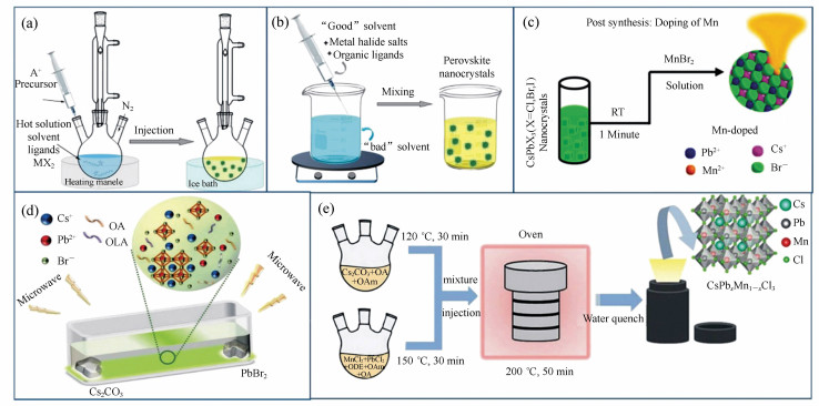
Colloidal Mn2+ doped CsPbX3(X=Cl, Br, I) nanocrystals(NCs) are being explored extensively as alternative emitting materials, wherein highly efficient optical and optoelectronic processes can be achieved. Mn2+ doping in perovskite NCs also reveals several new fundamental aspects of doping and new dopant-induced optical properties through different methods of synthesis. Mn2+ doping exists in wide-band-gap perovskite hosts where the excitation energy is transferred to an Mn d-state, resulting in short-range tunable yellow-orange d-d emissions. Enormous efforts have been expended on understanding the doping process and designing highly efficient doped NCs. The unique electronic and fluorescent properties endow these Mn2+ doped perovskite NCs with various optoelectronic applications in light-emitting diodes(LEDs) and solar cells. Combining all these facts, this review focuses on the recent progress in synthesis methods, emission mechanism, and potential applications of Mn2+ doped CsPbX3 perovskite NCs and provides an outline for plausible future studies.
Colloidal Mn2+ doped CsPbX3(X=Cl, Br, I) nanocrystals(NCs) are being explored extensively as alternative emitting materials, wherein highly efficient optical and optoelectronic processes can be achieved. Mn2+ doping in perovskite NCs also reveals several new fundamental aspects of doping and new dopant-induced optical properties through different methods of synthesis. Mn2+ doping exists in wide-band-gap perovskite hosts where the excitation energy is transferred to an Mn d-state, resulting in short-range tunable yellow-orange d-d emissions. Enormous efforts have been expended on understanding the doping process and designing highly efficient doped NCs. The unique electronic and fluorescent properties endow these Mn2+ doped perovskite NCs with various optoelectronic applications in light-emitting diodes(LEDs) and solar cells. Combining all these facts, this review focuses on the recent progress in synthesis methods, emission mechanism, and potential applications of Mn2+ doped CsPbX3 perovskite NCs and provides an outline for plausible future studies.
2019, 12(5): 952-963.
doi: 10.3788/CO.20191205.0952
Abstract:
The charge transfer(CT) process plays a key role in the operation of the optoelectronic device system so a better understanding of the interfacial CT property is greatly important. In this paper, Surface Enhanced Raman Scattering(SERS) was utilized to study the interfacial CT property between CuPc and perovskites(single crystal and polycrystalline). The Raman spectra of CuPc adsorbed on the perovskite surface was enhanced. The laser wavelength dependent SERS study indicates that this phenomenon is mainly arising from the CT from the VB band of perovskite to the LUMO band of the CuPc molecules. In comparison, the SERS signal of CuPc molecules adsorbed on a single crystal is much stronger than that on the polycrystalline perovskite. This result indicates that the defect status affects the enhancement ability of the materials. Further study shows that, after the decoration of a thin silver film, the SERS spectra of CuPc on both single crystal and polycrystalline perovskites are further enhanced. The extreme enhancement is not only due to the electromagnetic property of the silver film but also the fact that the SPR of the silver enhances the charge separation of the perovskite, which further promotes the CT process between the substrate and adsorbed molecules. The CT based SERS study shows great potential application value in the field of optoelectronic research.
The charge transfer(CT) process plays a key role in the operation of the optoelectronic device system so a better understanding of the interfacial CT property is greatly important. In this paper, Surface Enhanced Raman Scattering(SERS) was utilized to study the interfacial CT property between CuPc and perovskites(single crystal and polycrystalline). The Raman spectra of CuPc adsorbed on the perovskite surface was enhanced. The laser wavelength dependent SERS study indicates that this phenomenon is mainly arising from the CT from the VB band of perovskite to the LUMO band of the CuPc molecules. In comparison, the SERS signal of CuPc molecules adsorbed on a single crystal is much stronger than that on the polycrystalline perovskite. This result indicates that the defect status affects the enhancement ability of the materials. Further study shows that, after the decoration of a thin silver film, the SERS spectra of CuPc on both single crystal and polycrystalline perovskites are further enhanced. The extreme enhancement is not only due to the electromagnetic property of the silver film but also the fact that the SPR of the silver enhances the charge separation of the perovskite, which further promotes the CT process between the substrate and adsorbed molecules. The CT based SERS study shows great potential application value in the field of optoelectronic research.
2019, 12(5): 964-992.
doi: 10.3788/CO.20191205.0964
Abstract:
Organic-inorganic halide perovskite, as represented by CH3NH3PbI3, has been attracting increasing attention due to its advanced optoelectronic properties, such as suitable band gaps, high optical absorption, bipolar carrier conductivity, ultralong carrier diffusion length and appropriate exciton binding energy. At present, solar cells based on organic-inorganic halide perovskite have gained enormous significance and reached a power conversion efficiency exceeding 25%, which was less than 4% in 2009. In addition, combined with the low-cost solution spin-coating method for sample preparation, perovskite materials have become the focus of research in the field of novel solar cells. Researchers have been addressing the key challenges facing lead halide perovskites, including their stability and toxicity issues. In this paper, research progress on the optimal designs of halide perovskite photovoltaic materials is reviewed in detail, including single(AMX3), double(A2MM'X6), ordered-vacancy double(A2MX6), 2D(A'2An-1MnX3n+1) perovskites and perovskite-like(A3M2X9) materials. Through rational design, the material stability and toxicity of perovskites have been solved or improved to some extent but the photovoltaic performance has yet to be further optimized. In this research, the first-principles of high-throughput material simulation showed predictive ability in material design. The results of interactive feedback and mutual verification with experimental research were obtained. In addition, the problems introduced by new materials in rational designs are discussed and a powerful method for addressing these problems is proposed.
Organic-inorganic halide perovskite, as represented by CH3NH3PbI3, has been attracting increasing attention due to its advanced optoelectronic properties, such as suitable band gaps, high optical absorption, bipolar carrier conductivity, ultralong carrier diffusion length and appropriate exciton binding energy. At present, solar cells based on organic-inorganic halide perovskite have gained enormous significance and reached a power conversion efficiency exceeding 25%, which was less than 4% in 2009. In addition, combined with the low-cost solution spin-coating method for sample preparation, perovskite materials have become the focus of research in the field of novel solar cells. Researchers have been addressing the key challenges facing lead halide perovskites, including their stability and toxicity issues. In this paper, research progress on the optimal designs of halide perovskite photovoltaic materials is reviewed in detail, including single(AMX3), double(A2MM'X6), ordered-vacancy double(A2MX6), 2D(A'2An-1MnX3n+1) perovskites and perovskite-like(A3M2X9) materials. Through rational design, the material stability and toxicity of perovskites have been solved or improved to some extent but the photovoltaic performance has yet to be further optimized. In this research, the first-principles of high-throughput material simulation showed predictive ability in material design. The results of interactive feedback and mutual verification with experimental research were obtained. In addition, the problems introduced by new materials in rational designs are discussed and a powerful method for addressing these problems is proposed.
2019, 12(5): 993-1014.
doi: 10.3788/CO.20191205.0993
Abstract:
Perovskite has the advantages of high luminescence quantum yield and having a free carrier and a perfect crystal structure. It was first proposed for applications in the field of solar cells and has been rapidly developing in recent years. The direction of its research has gradually expanded to electroluminescence and lasers. In this paper, the research progress of perovskite materials in the laser field is introduced, which is mainly described from four perspectives:perovskite lasers with an adjustable wide wavelength range, perovskite lasers with high stability, perovskite lasers with ultraviolet light and new wavelength laser output potential, and perovskite lasers with nonlinear optical characteristics. Various preparation methods and optical properties of perovskite materials are listed. The structure characteristics and output mode of existing perovskite lasers are summarized and the existing barriers to the widespread application of perovskite materials in lasers are analyzed. This paper provides reference for further research on perovskite materials in the field of lasers.
Perovskite has the advantages of high luminescence quantum yield and having a free carrier and a perfect crystal structure. It was first proposed for applications in the field of solar cells and has been rapidly developing in recent years. The direction of its research has gradually expanded to electroluminescence and lasers. In this paper, the research progress of perovskite materials in the laser field is introduced, which is mainly described from four perspectives:perovskite lasers with an adjustable wide wavelength range, perovskite lasers with high stability, perovskite lasers with ultraviolet light and new wavelength laser output potential, and perovskite lasers with nonlinear optical characteristics. Various preparation methods and optical properties of perovskite materials are listed. The structure characteristics and output mode of existing perovskite lasers are summarized and the existing barriers to the widespread application of perovskite materials in lasers are analyzed. This paper provides reference for further research on perovskite materials in the field of lasers.
2019, 12(5): 1015-1027.
doi: 10.3788/CO.20191205.1015
Abstract:
Perovskite materials have the advantages of long carrier diffusion length, tunable band gap and high light absorption efficiency. Additionally, the storage of raw materials used in the production of perovskite solar cells is very rich and the formation energy required for the deposition process is low. Meanwhile, the production process is compatible with large-area manufacturing techniques. Low production cost, high conversion efficiency and wide application fields make the perovskite solar cells comparable to silicon-based solar cells. In today's perovskite research, high stability and large-area production are the research hotspots of photovoltaic technology. The research progress of the ink composition and process control of recent printing techniques are reviewed in this paper. The advantages and limitations of these methods are briefly described and compared. We focus on the factors that need to be considered in the production of perovskite solar cells, different preparation methods that can improve perovskite film quality and strategies for improving stability and applicability in industrial production.
Perovskite materials have the advantages of long carrier diffusion length, tunable band gap and high light absorption efficiency. Additionally, the storage of raw materials used in the production of perovskite solar cells is very rich and the formation energy required for the deposition process is low. Meanwhile, the production process is compatible with large-area manufacturing techniques. Low production cost, high conversion efficiency and wide application fields make the perovskite solar cells comparable to silicon-based solar cells. In today's perovskite research, high stability and large-area production are the research hotspots of photovoltaic technology. The research progress of the ink composition and process control of recent printing techniques are reviewed in this paper. The advantages and limitations of these methods are briefly described and compared. We focus on the factors that need to be considered in the production of perovskite solar cells, different preparation methods that can improve perovskite film quality and strategies for improving stability and applicability in industrial production.
2019, 12(5): 1028-1039.
doi: 10.3788/CO.20191205.1028
Abstract:
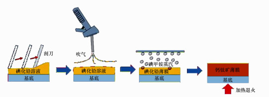
Perovskite solar cells(PSCs) have attracted widespread attention due to their high efficiency and easy preparation with solution method. Normally, perovskite thin films are prepared via spin coating. Spin coating is not suitable for large-area preparation due to its drawbacks, including nonuniformity of film thickness and excessive waste of materials. Large-area preparation of uniform perovskite solar cells is still a big challenge today. Therefore, a vapor-assisted doctor blading(VADB) process is demonstrated here to prepare large-area and highly crystallized perovskite thin films. In addition, by changing the concentration of the precursor solution, perovskite films of different thicknesses are produced. Furthermore, we find that the performance of PSCs with a precursor concentration of 1.0 M is the best. The devices show the highest efficiencies of 17.76%(average 16.9%) and 16.3% under simulated AM1.5G(100 mW/cm2) solar light on an active area of 0.112 5 cm2 and 1.0 cm2, respectively. This provides a new possible way for the large-area preparation of PSCs.
Perovskite solar cells(PSCs) have attracted widespread attention due to their high efficiency and easy preparation with solution method. Normally, perovskite thin films are prepared via spin coating. Spin coating is not suitable for large-area preparation due to its drawbacks, including nonuniformity of film thickness and excessive waste of materials. Large-area preparation of uniform perovskite solar cells is still a big challenge today. Therefore, a vapor-assisted doctor blading(VADB) process is demonstrated here to prepare large-area and highly crystallized perovskite thin films. In addition, by changing the concentration of the precursor solution, perovskite films of different thicknesses are produced. Furthermore, we find that the performance of PSCs with a precursor concentration of 1.0 M is the best. The devices show the highest efficiencies of 17.76%(average 16.9%) and 16.3% under simulated AM1.5G(100 mW/cm2) solar light on an active area of 0.112 5 cm2 and 1.0 cm2, respectively. This provides a new possible way for the large-area preparation of PSCs.
2019, 12(5): 1040-1047.
doi: 10.3788/CO.20191205.1040
Abstract:
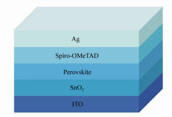
The electron transport layer(ETL) plays a crucial role in carrier extraction and transportation in perovskite solar cells. Tin(Ⅳ) oxide is widely used as ETL-material in planar perovskite solar cells due to its excellent properties. However, current processes for tin oxide film preparation can hardly meet industrial requirements, such as large-scale and automatic fabrication. Therefore, developing a new fabrication method suitable for industrialization is in urgent demanded. To solve this problem, a high-quality tin oxide film was successfully created using the spray coating method. Experimental results show that the performance of the perovskite solar cells is highly dependent on the thickness of the spray-coated tin oxide film. By optimizing film thickness, power conversion efficiency(PCE) can be improved to 15.72%. The film exhibits a coffee ring phenomenon, which increases the series resistance and limits the PCE. That can be solved by further decreasing the size of the droplets. This paper demonstrates a new method for the fabrication of high-quality, highly adaptable tin oxide films for the industrialization of perovskite solar cells.
The electron transport layer(ETL) plays a crucial role in carrier extraction and transportation in perovskite solar cells. Tin(Ⅳ) oxide is widely used as ETL-material in planar perovskite solar cells due to its excellent properties. However, current processes for tin oxide film preparation can hardly meet industrial requirements, such as large-scale and automatic fabrication. Therefore, developing a new fabrication method suitable for industrialization is in urgent demanded. To solve this problem, a high-quality tin oxide film was successfully created using the spray coating method. Experimental results show that the performance of the perovskite solar cells is highly dependent on the thickness of the spray-coated tin oxide film. By optimizing film thickness, power conversion efficiency(PCE) can be improved to 15.72%. The film exhibits a coffee ring phenomenon, which increases the series resistance and limits the PCE. That can be solved by further decreasing the size of the droplets. This paper demonstrates a new method for the fabrication of high-quality, highly adaptable tin oxide films for the industrialization of perovskite solar cells.
2019, 12(5): 1048-1056.
doi: 10.3788/CO.20191205.1048
Abstract:
In order to obtain excellent perovskite materials, we systematically investigate the structural, electronic and optical properties of perovskites and the influence of vacancy defects on their optical properties. First, we explore the structural properties of intrinsic perovskites via Materials Studio and use the Generalized Gradient Approximation(GGA) with the Perdew-Burke-Ernzerhof(PBE) function to optimize the crystal structure and calculate the electronic or optical properties. To obtain accurate bandgap, we use Density Functional Theory-Vander Waals Force(DFT-VDW) correlations to explain the underestimated bandgap. The investigations of the different vacancy defects in perovskites are then carried out and the band structure, density of states and optical properties are measured. Finally, the properties of self-doped perovskites with vacancy defects are further investigated with comparison to the properties of intrinsic perovskites. Our results indicate that the obtained bandgap of intrinsic perovskites was 1.52 eV, which is consistent with the experimental value. The perovskites with Pb vacancy defects belong to P-type materials and those with I vacancy defects belong to N-type materials. The dielectric virtual function and absorption spectrum exhibit substantial change, which has important theoretical value for the physical properties of perovskites and their applications in the fields of optoelectronic devices.
In order to obtain excellent perovskite materials, we systematically investigate the structural, electronic and optical properties of perovskites and the influence of vacancy defects on their optical properties. First, we explore the structural properties of intrinsic perovskites via Materials Studio and use the Generalized Gradient Approximation(GGA) with the Perdew-Burke-Ernzerhof(PBE) function to optimize the crystal structure and calculate the electronic or optical properties. To obtain accurate bandgap, we use Density Functional Theory-Vander Waals Force(DFT-VDW) correlations to explain the underestimated bandgap. The investigations of the different vacancy defects in perovskites are then carried out and the band structure, density of states and optical properties are measured. Finally, the properties of self-doped perovskites with vacancy defects are further investigated with comparison to the properties of intrinsic perovskites. Our results indicate that the obtained bandgap of intrinsic perovskites was 1.52 eV, which is consistent with the experimental value. The perovskites with Pb vacancy defects belong to P-type materials and those with I vacancy defects belong to N-type materials. The dielectric virtual function and absorption spectrum exhibit substantial change, which has important theoretical value for the physical properties of perovskites and their applications in the fields of optoelectronic devices.
2019, 12(5): 1057-1063.
doi: 10.3788/CO.20191205.1057
Abstract:
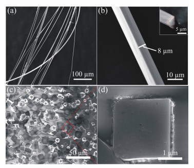
Efficient and stable p-type doping is difficult to achieve. To solve this problem, high-quality p-type Se microwires were fabricated using chemical vapor deposition. A photodetector based on a single Se microtube shows broadband photoresponses with a peak responsivity of 2.8 mA/W at 600 nm under 5 V bias. The cutoff wavelength is estimated to be 675 nm. A p-n heterojunction photodetector using a p-type Se microwire and n-type CH3NH3PbCl3 was also fabricated. Compared to the single Se microtube, the p-n heterojunction photodetector shows obvious reduction in response time and 850% improvement in responsivity. The experimental results indicate that p-n junctions have promising applications in high-performance photodetectors.
Efficient and stable p-type doping is difficult to achieve. To solve this problem, high-quality p-type Se microwires were fabricated using chemical vapor deposition. A photodetector based on a single Se microtube shows broadband photoresponses with a peak responsivity of 2.8 mA/W at 600 nm under 5 V bias. The cutoff wavelength is estimated to be 675 nm. A p-n heterojunction photodetector using a p-type Se microwire and n-type CH3NH3PbCl3 was also fabricated. Compared to the single Se microtube, the p-n heterojunction photodetector shows obvious reduction in response time and 850% improvement in responsivity. The experimental results indicate that p-n junctions have promising applications in high-performance photodetectors.
2019, 12(5): 1064-1075.
doi: 10.3788/CO.20191205.1064
Abstract:
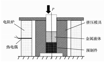
Compared to traditional alloys, medium/high volume fraction SiCp/Al composites offer tailorable mechanical and thermophysical properties that could be beneficial for a variety of applications. In this paper, the main fabrication methods and applications of medium/high volume fraction SiCp/Al composites in precision instruments, optical systems, electronic packaging and thermal control are reviewed and summarized. Finally, the future development strategy of medium/high volume fraction SiCp/Al is proposed.
Compared to traditional alloys, medium/high volume fraction SiCp/Al composites offer tailorable mechanical and thermophysical properties that could be beneficial for a variety of applications. In this paper, the main fabrication methods and applications of medium/high volume fraction SiCp/Al composites in precision instruments, optical systems, electronic packaging and thermal control are reviewed and summarized. Finally, the future development strategy of medium/high volume fraction SiCp/Al is proposed.
2019, 12(5): 1076-1089.
doi: 10.3788/CO.20191205.1076
Abstract:
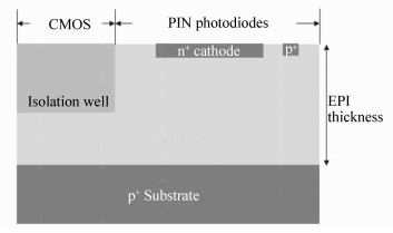
Traditional CMOS image sensors generally use PN photodiodes or PPDs as the photosensitive element, which are formed based on N-well/P-type substrates using the LV-CMOS process. The PIN photosensitive element has small junction capacitance and high quantum efficiency. By using High-Voltage CMOS(HV-CMOS), monolithic integration of CMOS circuits with PIN photodiodes can be achieved. In this paper, the relationship between the photo-response characteristics, NEP of CMOS detectors and pixel size and reset voltage are studied. The results show that the pixel charge gain can be increased by about one order of magnitude when the photosensitive element is changed from PN to PIN and the transient charge gain of the pixel is larger than 1/Cpd. This is closely related to the size of the diode and reset voltage. It is found that small pixels are more suitable for fast detection of short integration time under weak signals because of their higher charge gain and lower equivalent noise. If combined with microlenses, small pixels can be further advantageous in low light detection.
Traditional CMOS image sensors generally use PN photodiodes or PPDs as the photosensitive element, which are formed based on N-well/P-type substrates using the LV-CMOS process. The PIN photosensitive element has small junction capacitance and high quantum efficiency. By using High-Voltage CMOS(HV-CMOS), monolithic integration of CMOS circuits with PIN photodiodes can be achieved. In this paper, the relationship between the photo-response characteristics, NEP of CMOS detectors and pixel size and reset voltage are studied. The results show that the pixel charge gain can be increased by about one order of magnitude when the photosensitive element is changed from PN to PIN and the transient charge gain of the pixel is larger than 1/Cpd. This is closely related to the size of the diode and reset voltage. It is found that small pixels are more suitable for fast detection of short integration time under weak signals because of their higher charge gain and lower equivalent noise. If combined with microlenses, small pixels can be further advantageous in low light detection.
2019, 12(5): 1090-1099.
doi: 10.3788/CO.20191205.1090
Abstract:
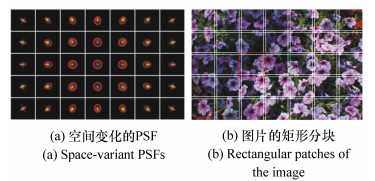
In order to meet requirements of the low cost and miniaturization of high-quality cameras, an optical/algorithmic co-design method for a large-field simple optical system is proposed. The residual aberrations of this simple optical system are corrected using an image restoration algorithm. Firstly, spatially varying cross-channel deconvolution is improved for large-field optical systems, wherein correction of lateral chromatic aberrations is introduced so that they can be significantly removed through the image restoration algorithm. Then, when designing the optical system, the constraints of chromatic aberrations are removed and we concentrate on optimizing the quality of the green channel to make the image sharp, which will help the restoration of images in the red and the blue channels in later cross-channel deconvolution. Using this method, a large-field simple optical system with two lenses of the same material is designed. The focal length of the system is 50 mm, the full field is 46 degrees, the F number is 5.6 and the resolution of the sensor is 10 mega pixels. Experimental results indicate that the image quality of the proposed simple large-field optical system is comparable to that when using a Cooke triplet lens and is better than that when using pure image restoration algorithms. Our proposed method succeeds as a simple large-field optical system and can obtain high-resolution and high-quality images.
In order to meet requirements of the low cost and miniaturization of high-quality cameras, an optical/algorithmic co-design method for a large-field simple optical system is proposed. The residual aberrations of this simple optical system are corrected using an image restoration algorithm. Firstly, spatially varying cross-channel deconvolution is improved for large-field optical systems, wherein correction of lateral chromatic aberrations is introduced so that they can be significantly removed through the image restoration algorithm. Then, when designing the optical system, the constraints of chromatic aberrations are removed and we concentrate on optimizing the quality of the green channel to make the image sharp, which will help the restoration of images in the red and the blue channels in later cross-channel deconvolution. Using this method, a large-field simple optical system with two lenses of the same material is designed. The focal length of the system is 50 mm, the full field is 46 degrees, the F number is 5.6 and the resolution of the sensor is 10 mega pixels. Experimental results indicate that the image quality of the proposed simple large-field optical system is comparable to that when using a Cooke triplet lens and is better than that when using pure image restoration algorithms. Our proposed method succeeds as a simple large-field optical system and can obtain high-resolution and high-quality images.
2019, 12(5): 1100-1108.
doi: 10.3788/CO.20191205.1100
Abstract:
To prove the reciprocity of an atmospheric turbulent channel in bidirectional optical transmission systems, we propose a method for measuring the correlation between the fading of instantaneously received signals and establish a mathematical model for analyzing the measurement data. Experiments of bidirectional optical transmission measurements were carried out between two tall buildings separated by 883 m. According to the measured speckle image data, we verified the instantaneous-fading correlation of the channel and analyzed the effect of the normalized received signal fluctuation variance on the correlation coefficient in practical scenarios. It was shown that most of the instantaneous-fading correlation coefficients of optical channels in the two counter-directions were above 0.85 and even up to 0.95, which proves that reciprocity can be well maintained for a bidirectional turbulent optical channel. With an increasing fluctuation variance of the normalized received optical signal, the correlation coefficient is slightly descending.
To prove the reciprocity of an atmospheric turbulent channel in bidirectional optical transmission systems, we propose a method for measuring the correlation between the fading of instantaneously received signals and establish a mathematical model for analyzing the measurement data. Experiments of bidirectional optical transmission measurements were carried out between two tall buildings separated by 883 m. According to the measured speckle image data, we verified the instantaneous-fading correlation of the channel and analyzed the effect of the normalized received signal fluctuation variance on the correlation coefficient in practical scenarios. It was shown that most of the instantaneous-fading correlation coefficients of optical channels in the two counter-directions were above 0.85 and even up to 0.95, which proves that reciprocity can be well maintained for a bidirectional turbulent optical channel. With an increasing fluctuation variance of the normalized received optical signal, the correlation coefficient is slightly descending.
2019, 12(5): 1109-1117.
doi: 10.3788/CO.20191205.1109
Abstract:
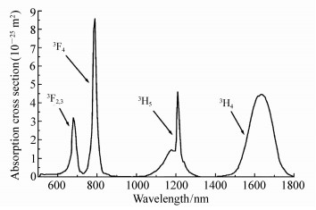
The optical fibers and devices used in thulium-doped fiber lasers(TDFL) are mostly produced by foreign companies. Therefore, it is necessary to develop TDFL based on homemade materials and devices. In this paper, the performance of continuous-wave thulium-doped fiber oscillators using a homemade gain fiber is reported. During the experiment, using a domestic thulium-doped fiber with a core diameter of 10 μm, homemade LD(laser diode) pump sources and fiber gratings, three oscillators were developed to generate laser output with central wavelengths of 1 918 nm, 1 941 nm and 2 013 nm, respectively. In addition, the laser output characteristics of the homemade and imported thulium-doped gain fibers were compared. The experimental results indicate that the output efficiency of the homemade thulium-doped fiber(TDF) is 6-11% lower than the imported TDF, but the homemade TDF has a similar spectral linewidth(about 0.1 nm) and a better near-field spot.
The optical fibers and devices used in thulium-doped fiber lasers(TDFL) are mostly produced by foreign companies. Therefore, it is necessary to develop TDFL based on homemade materials and devices. In this paper, the performance of continuous-wave thulium-doped fiber oscillators using a homemade gain fiber is reported. During the experiment, using a domestic thulium-doped fiber with a core diameter of 10 μm, homemade LD(laser diode) pump sources and fiber gratings, three oscillators were developed to generate laser output with central wavelengths of 1 918 nm, 1 941 nm and 2 013 nm, respectively. In addition, the laser output characteristics of the homemade and imported thulium-doped gain fibers were compared. The experimental results indicate that the output efficiency of the homemade thulium-doped fiber(TDF) is 6-11% lower than the imported TDF, but the homemade TDF has a similar spectral linewidth(about 0.1 nm) and a better near-field spot.
2019, 12(5): 1118-1123.
doi: 10.3788/CO.20191205.1118
Abstract:
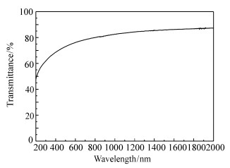
In order to determine the latent function of an Na5[B2P3O13] crystal, its ultraviolet-far-infrared spectra and Raman spectra are studied. The ultraviolet-visible-infrared and far-infrared spectra and Raman spectra of an Na5[B2P3O13] crystal were measured at room temperature in the range of 200 to 2 000 nm and in the range of 50 to 4 000 cm-1. The results show that the maximum absorption coefficient is 3.1 cm-1, the extinction coefficient is in the order of 10-6 and the refractive index is 1.56 to 1.80. Its Sellmeier equation is then obtained. In the frequency ranges of 105 to 120 THz and 150 to 375 THz, the transmittance is more than 80%, but in the frequency range of 1.5 to 71 THz, the transmittance is nearly zero. It is possible that the Na5[B2P3O13] crystal can be used as an optical window material or filter in some frequency ranges.
In order to determine the latent function of an Na5[B2P3O13] crystal, its ultraviolet-far-infrared spectra and Raman spectra are studied. The ultraviolet-visible-infrared and far-infrared spectra and Raman spectra of an Na5[B2P3O13] crystal were measured at room temperature in the range of 200 to 2 000 nm and in the range of 50 to 4 000 cm-1. The results show that the maximum absorption coefficient is 3.1 cm-1, the extinction coefficient is in the order of 10-6 and the refractive index is 1.56 to 1.80. Its Sellmeier equation is then obtained. In the frequency ranges of 105 to 120 THz and 150 to 375 THz, the transmittance is more than 80%, but in the frequency range of 1.5 to 71 THz, the transmittance is nearly zero. It is possible that the Na5[B2P3O13] crystal can be used as an optical window material or filter in some frequency ranges.
2019, 12(5): 1124-1130.
doi: 10.3788/CO.20191205.1124
Abstract:
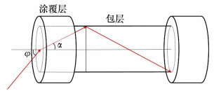
In fiber lasers, there are cladding lights with different transmission angles. In order to study the stripping effects of corroded cladding light strippers(CLS) on cladding light at various angles, we measured the scattering coefficient of the corroded section of the fiber. Meanwhile, we also simulated the relationship between the attenuation and the corrosion length of the cladding light at different transmission angles. To produce cladding light at different angles, we built two sets of stripper test systems:one to test the CLS made of double-clad fiber and one to test the coreless fiber. In the double-clad fiber experiment, the maximum transmission angle of the two-system cladding light was changed from 10° to 3°12' and from 8° to 3°1'. These angles deviate from the maximum transmission angle of light in the core by 2°27'. In the coreless fiber experiment, the maximum transmission angle of the two-system cladding light was changed from 11° to 2°9' and from 8° to 2°12'. The maximum transmission angle approaches 0° as the cladding light attenuation increases. Finally, we tested the corroded cladding light stripper made of double-clad fiber on the tandem-pumped laser with a wavelength of 1 018 nm. The cladding light attenuation was 18.3 dB at an input power of 1 136 W.
In fiber lasers, there are cladding lights with different transmission angles. In order to study the stripping effects of corroded cladding light strippers(CLS) on cladding light at various angles, we measured the scattering coefficient of the corroded section of the fiber. Meanwhile, we also simulated the relationship between the attenuation and the corrosion length of the cladding light at different transmission angles. To produce cladding light at different angles, we built two sets of stripper test systems:one to test the CLS made of double-clad fiber and one to test the coreless fiber. In the double-clad fiber experiment, the maximum transmission angle of the two-system cladding light was changed from 10° to 3°12' and from 8° to 3°1'. These angles deviate from the maximum transmission angle of light in the core by 2°27'. In the coreless fiber experiment, the maximum transmission angle of the two-system cladding light was changed from 11° to 2°9' and from 8° to 2°12'. The maximum transmission angle approaches 0° as the cladding light attenuation increases. Finally, we tested the corroded cladding light stripper made of double-clad fiber on the tandem-pumped laser with a wavelength of 1 018 nm. The cladding light attenuation was 18.3 dB at an input power of 1 136 W.
2019, 12(5): 1131-1138.
doi: 10.3788/CO.20191205.1131
Abstract:
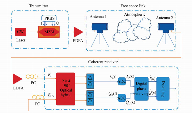
In recent years, the dilemma regarding the limited performance of coherent free-space optical(CFSO) communication with phase modulation caused by the phase fluctuations and intensity scintillations associated with atmospheric turbulence has gradually become the focus of research. In order to improve system performance, a CFSO communication system with quadrature phase-shift keying modulation(QPSK) is studied in this paper. With consideration of log-normal amplitude fluctuations and Gaussian distribution conditions, a two-stage joint carrier phase recovery(CPR) algorithm is proposed. With this scheme, the simulation results show that the phase noise of the system can be greatly reduced and its symbol error rate is three orders lower than that of the single-stage M-th power CPR algorithm. Therefore, the two-stage joint CPR algorithm holds significant improvement in CFSO communication systems.
In recent years, the dilemma regarding the limited performance of coherent free-space optical(CFSO) communication with phase modulation caused by the phase fluctuations and intensity scintillations associated with atmospheric turbulence has gradually become the focus of research. In order to improve system performance, a CFSO communication system with quadrature phase-shift keying modulation(QPSK) is studied in this paper. With consideration of log-normal amplitude fluctuations and Gaussian distribution conditions, a two-stage joint carrier phase recovery(CPR) algorithm is proposed. With this scheme, the simulation results show that the phase noise of the system can be greatly reduced and its symbol error rate is three orders lower than that of the single-stage M-th power CPR algorithm. Therefore, the two-stage joint CPR algorithm holds significant improvement in CFSO communication systems.
2019, 12(5): 1139-1146.
doi: 10.3788/CO.20191205.1139
Abstract:
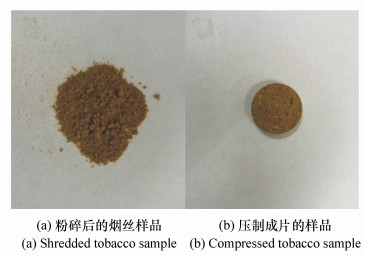
Different types of tobacco differ in element type and content. Based on Laser-Induced Breakdown Spectroscopy(LIBS), the atomic spectra were collected to realize fast classification and identification of different tobacco species combined with a support vector machine. In this paper, 9 kinds of cigarettes of different brands were selected and all characteristic peaks of spectral lines were extracted separately. Before classification, all feature peaks need to be preprocessed through multiple methods, including window smoothing to remove background and peak shift correction. After this, principal component analysis was used to reduce the dimension and the support vector machine method(SVM) was used to establish the classification model. Finally, classification results of 9 brands of cigarettes were obtained, with an average accuracy of 97.47%. It was proven that LIBS has great potential for applications in tobacco rapid identification, anti-counterfeiting identification and on-site rapid classification.
Different types of tobacco differ in element type and content. Based on Laser-Induced Breakdown Spectroscopy(LIBS), the atomic spectra were collected to realize fast classification and identification of different tobacco species combined with a support vector machine. In this paper, 9 kinds of cigarettes of different brands were selected and all characteristic peaks of spectral lines were extracted separately. Before classification, all feature peaks need to be preprocessed through multiple methods, including window smoothing to remove background and peak shift correction. After this, principal component analysis was used to reduce the dimension and the support vector machine method(SVM) was used to establish the classification model. Finally, classification results of 9 brands of cigarettes were obtained, with an average accuracy of 97.47%. It was proven that LIBS has great potential for applications in tobacco rapid identification, anti-counterfeiting identification and on-site rapid classification.
2019, 12(5): 1147-1154.
doi: 10.3788/CO.20191205.1147
Abstract:
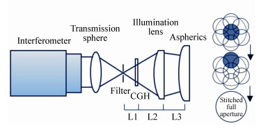
In order to achieve high-accuracy measurements of ultra-large aperture convex aspheric mirrors, a modified surface testing method is proposed. This method combines a Computer-Generated Hologram(CGH) and an illumination lens to create highly accurate and efficient measurements for ultra-large convex aspheres. Firstly, the basic principles of the method are researched. Then, a simulation is performed for an aspheric mirror with an aperture of 800 mm and a subaperture plan and CGH are designed. Finally, the sensitivity of this configuration is analyzed. Simulation results indicate that the residual aberrations are less than 0.001 3 nm RMS and that the accuracy of this testing method can be greater than 6 nm RMS. This method can satisfy the requirements for high accuracy surface testing in ultra-large convex aspheric surfaces.
In order to achieve high-accuracy measurements of ultra-large aperture convex aspheric mirrors, a modified surface testing method is proposed. This method combines a Computer-Generated Hologram(CGH) and an illumination lens to create highly accurate and efficient measurements for ultra-large convex aspheres. Firstly, the basic principles of the method are researched. Then, a simulation is performed for an aspheric mirror with an aperture of 800 mm and a subaperture plan and CGH are designed. Finally, the sensitivity of this configuration is analyzed. Simulation results indicate that the residual aberrations are less than 0.001 3 nm RMS and that the accuracy of this testing method can be greater than 6 nm RMS. This method can satisfy the requirements for high accuracy surface testing in ultra-large convex aspheric surfaces.


 Abstract
 FullText HTML
 PDF 5460KB