2021 Vol. 14, No. 1

 Abstract
 FullText HTML
 PDF 225KB
2021, 14(1): 1-17.
doi: 10.37188/CO.2020-0176
cstr: 32171.14.CO.2020-0176
Abstract:
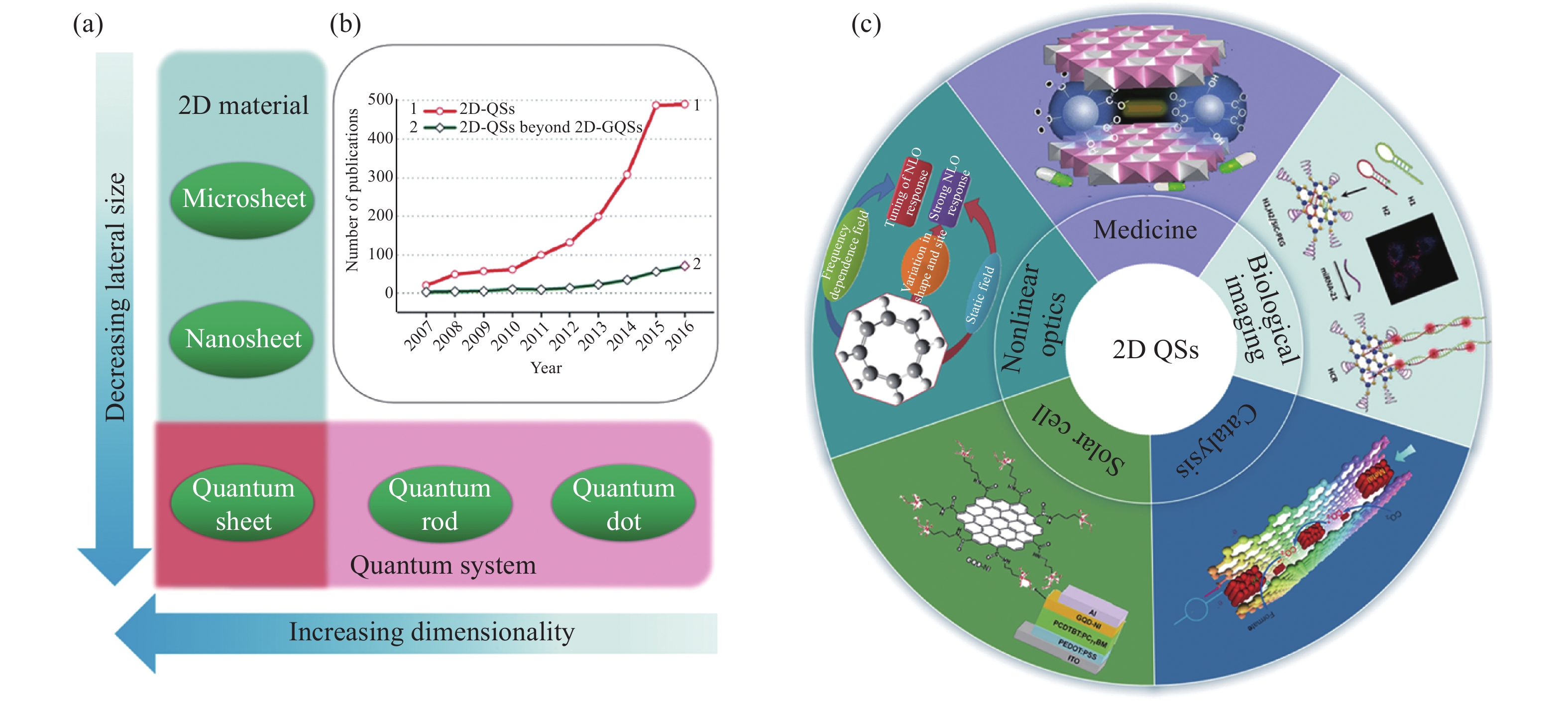
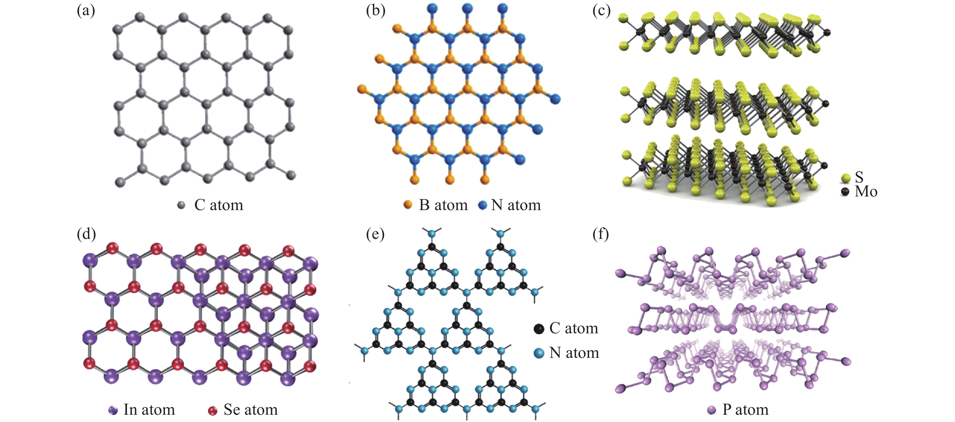
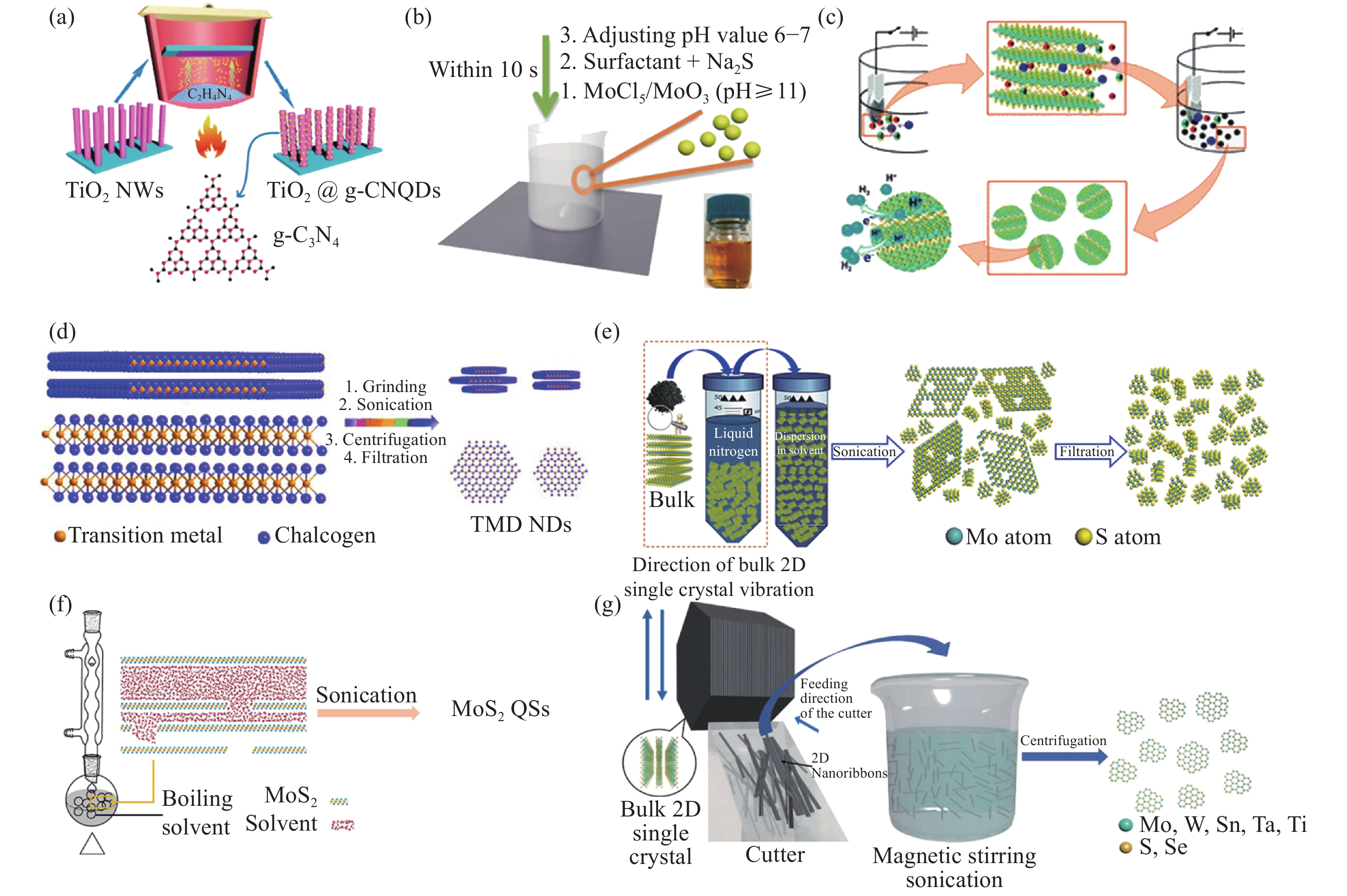
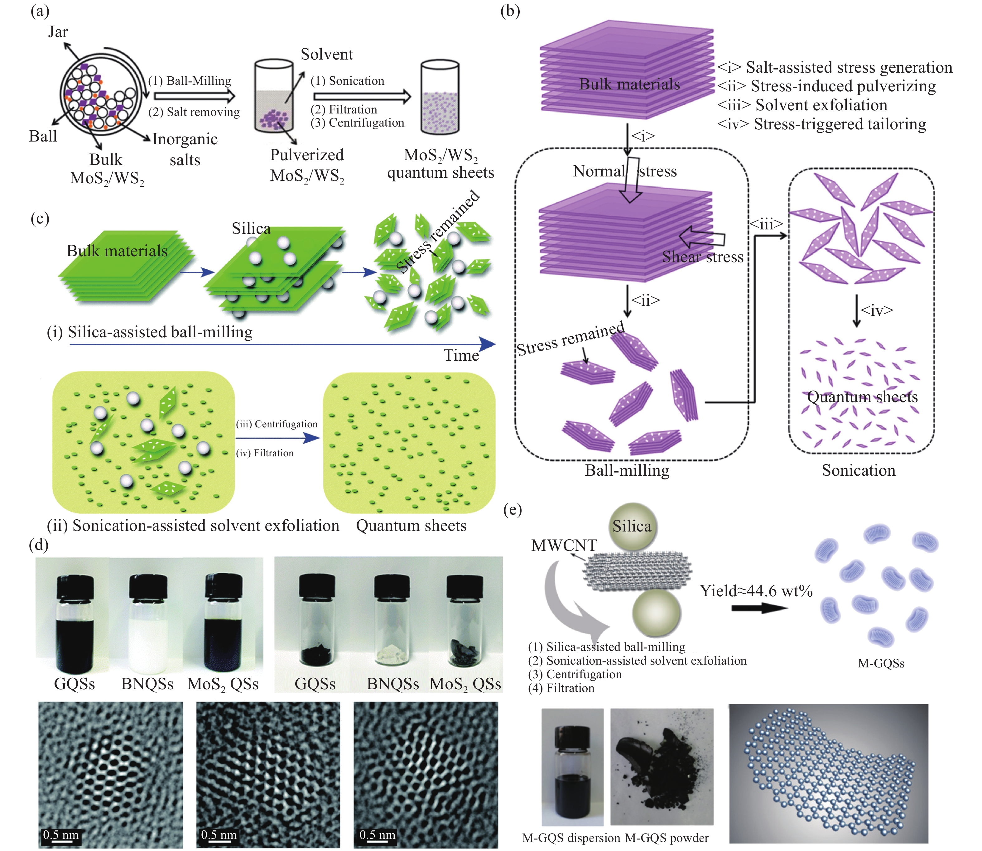
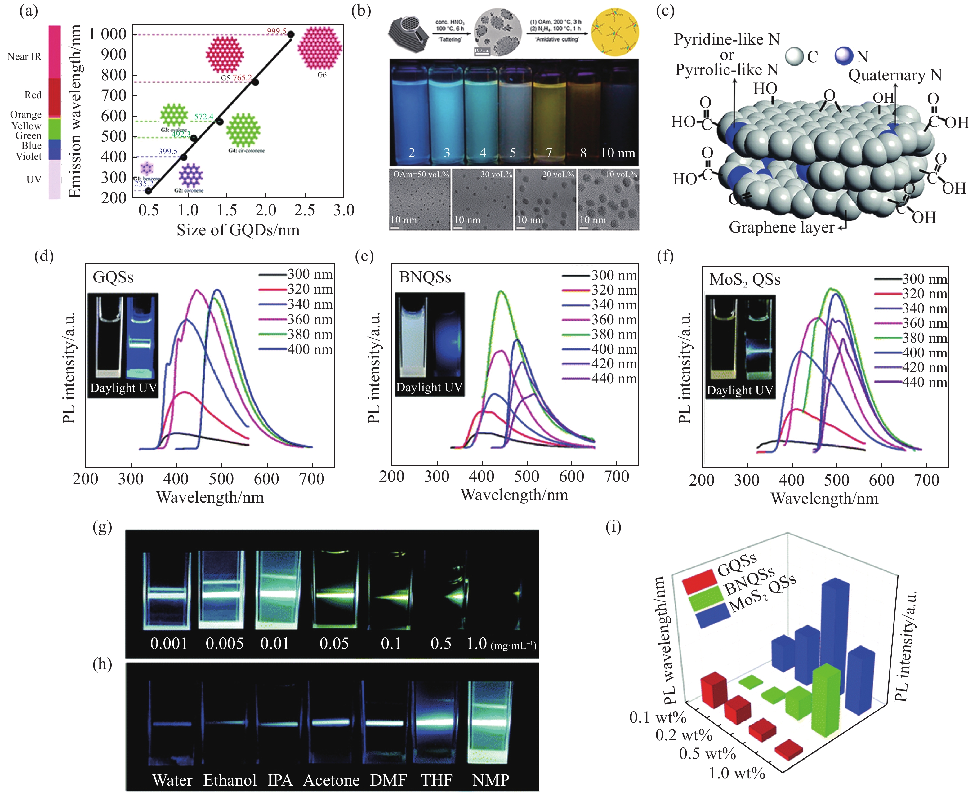
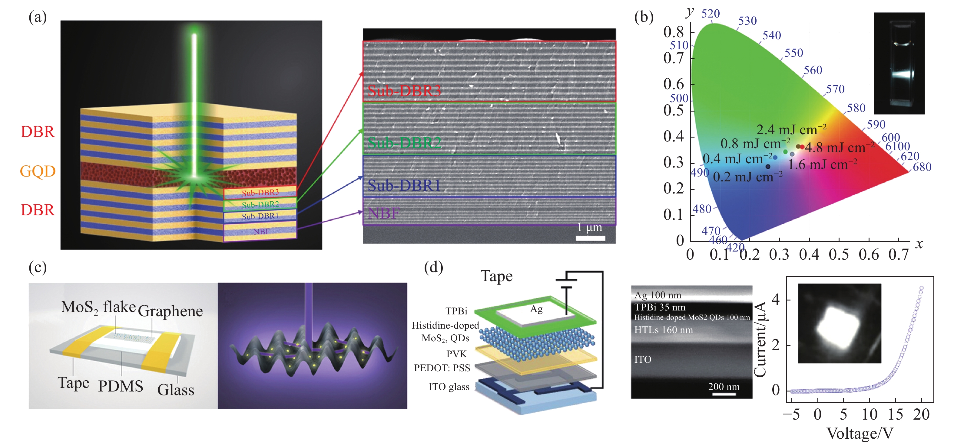
Two-dimensional (2D) materials like graphene have attracted much attention due to their unique structures and exotic properties. With significantly reduced lateral sizes, 2D quantum sheets (2D QSs) are attracting an increasing level of interest. 2D QSs have opportunities for new applications because of their intrinsic characteristics of being 2D materials and having emerging quantum confinement and prominent edge effects. This review focuses on the conceptual interpretation of 2D QSs and the recent progress on their preparation and optical properties. Particular focus is given to the realization and significance of the universal and scalable production of intrinsic 2D QSs. In addition, the photoluminescence of 2D QSs and their applications in nonlinear optics and solid-state light-emitting devices are reviewed. At the end, the perspectives and challenges towards the future development of 2D QSs are discussed.
Two-dimensional (2D) materials like graphene have attracted much attention due to their unique structures and exotic properties. With significantly reduced lateral sizes, 2D quantum sheets (2D QSs) are attracting an increasing level of interest. 2D QSs have opportunities for new applications because of their intrinsic characteristics of being 2D materials and having emerging quantum confinement and prominent edge effects. This review focuses on the conceptual interpretation of 2D QSs and the recent progress on their preparation and optical properties. Particular focus is given to the realization and significance of the universal and scalable production of intrinsic 2D QSs. In addition, the photoluminescence of 2D QSs and their applications in nonlinear optics and solid-state light-emitting devices are reviewed. At the end, the perspectives and challenges towards the future development of 2D QSs are discussed.

2021, 14(1): 18-42.
doi: 10.37188/CO.2020-0106
cstr: 32171.14.CO.2020-0106
Abstract:
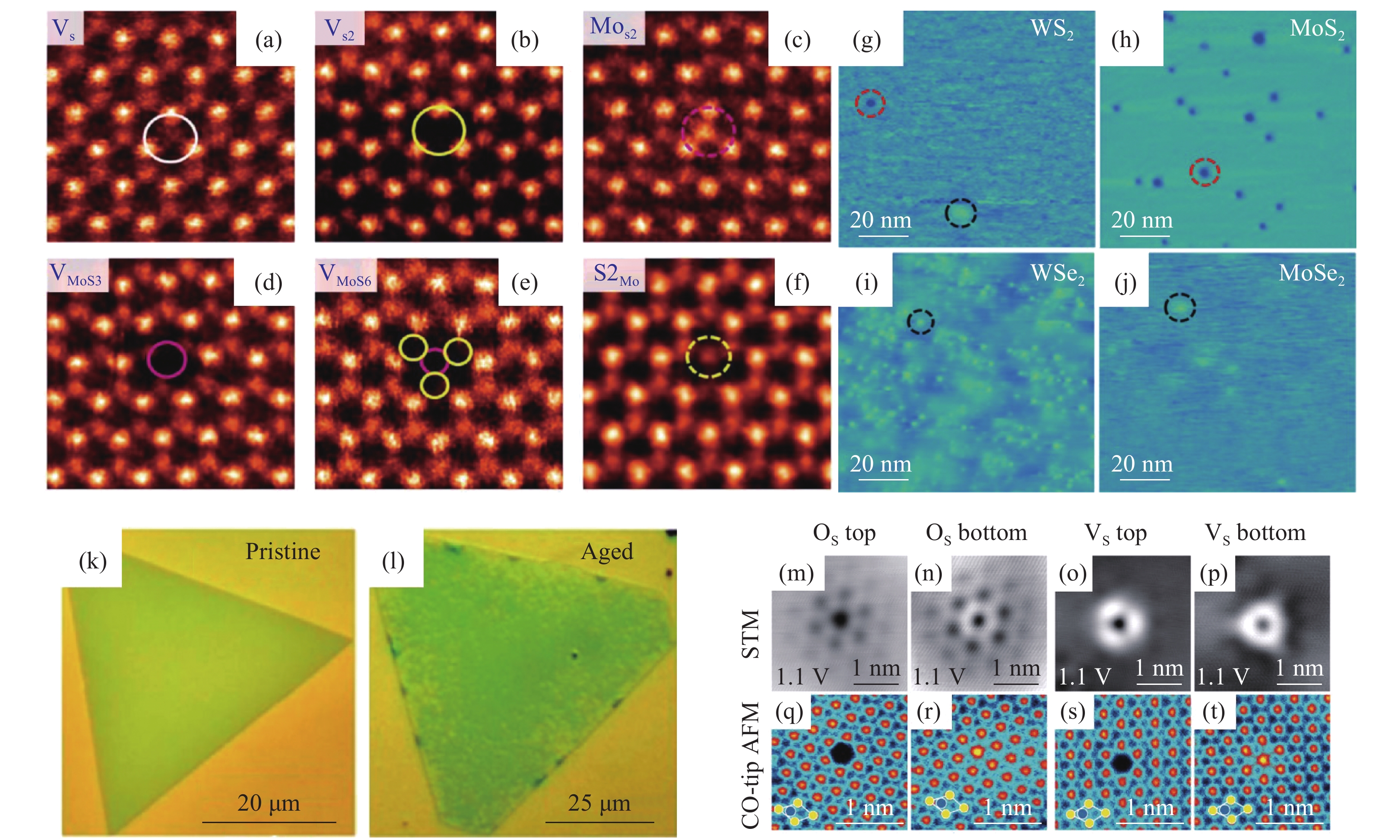
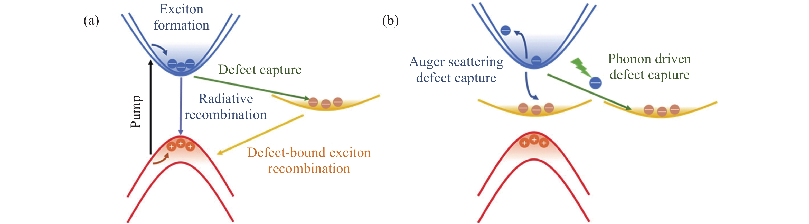
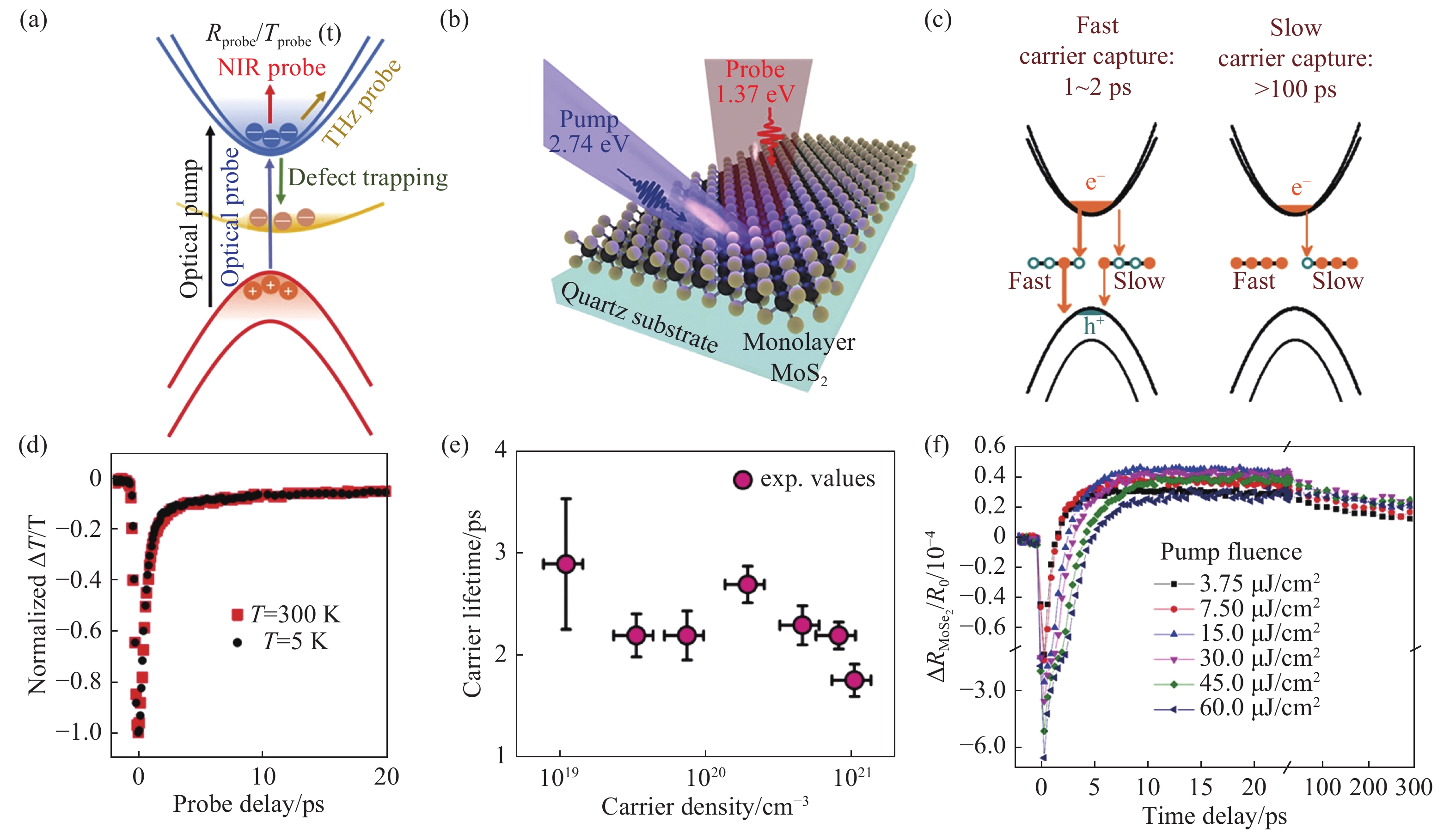
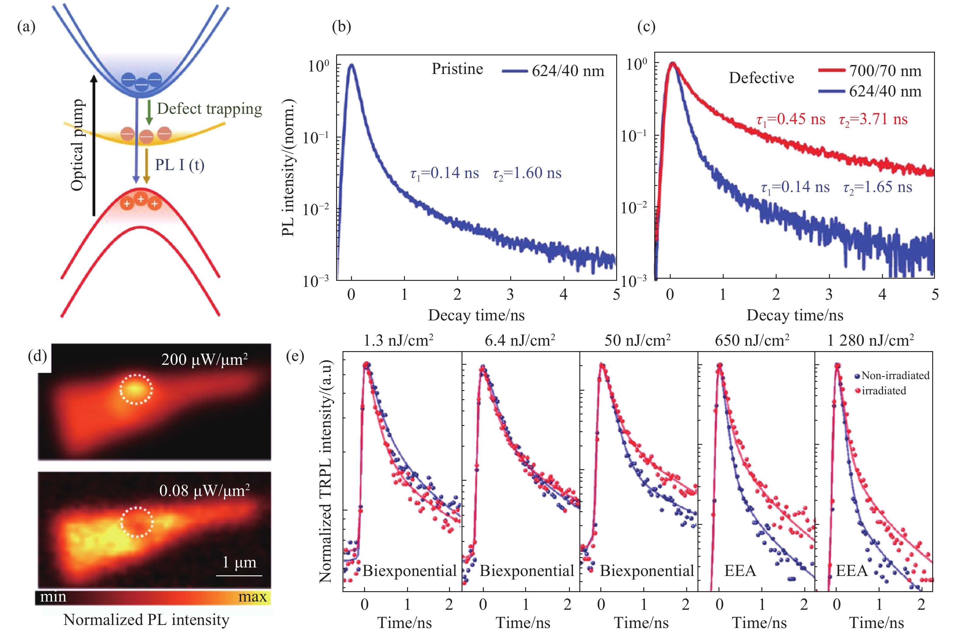
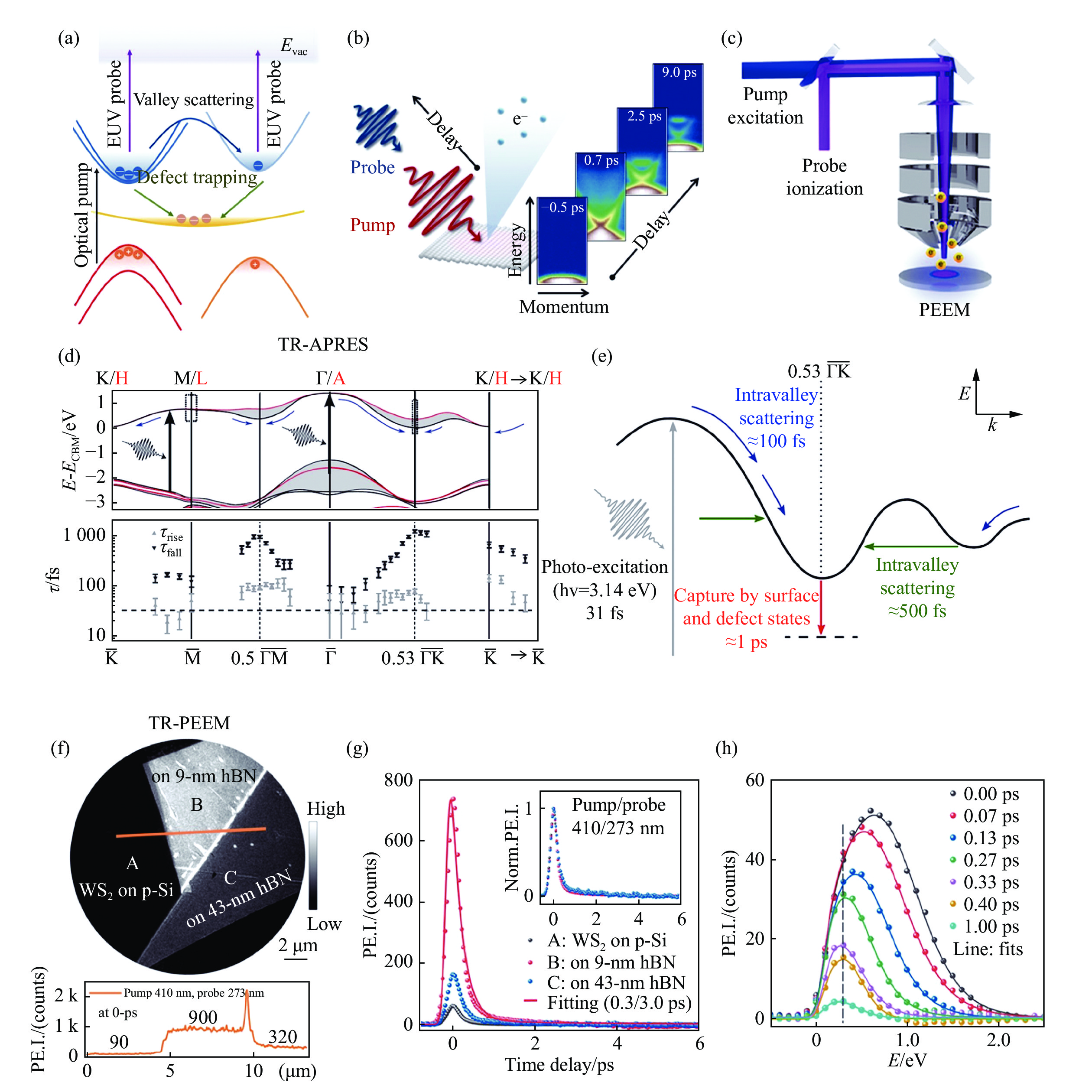
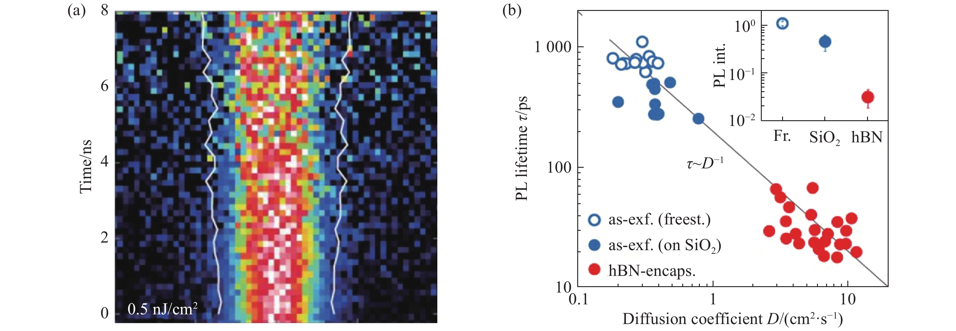
Because of their unique physical properties, the monolayer and few-layer two-dimensional transition metal chalcogenides with atomic-level thickness are expected to play an important role in the next generation of optoelectronic devices. However, defects in two-dimensional materials affect their properties to a great extent. On one hand, defects reduce the fluorescence quantum efficiency, carrier mobility and other important device parameters. On the other hand, the control and utilization of defects have given birth to new techniques such as using single-photon sources. Therefore, it is very important to characterize, understand, handle and control the defects in two-dimensional materials. In this review, the research progress on defects and its related carrier dynamics in two-dimensional transition metal chalcogenides is summarized. This paper aims to sort out the great influence of defects and their related ultrafast dynamics on material performance in two-dimensional transition metal chalcogenides, and to support studies on fundamental physical properties and high-performance optoelectronic devices.
Because of their unique physical properties, the monolayer and few-layer two-dimensional transition metal chalcogenides with atomic-level thickness are expected to play an important role in the next generation of optoelectronic devices. However, defects in two-dimensional materials affect their properties to a great extent. On one hand, defects reduce the fluorescence quantum efficiency, carrier mobility and other important device parameters. On the other hand, the control and utilization of defects have given birth to new techniques such as using single-photon sources. Therefore, it is very important to characterize, understand, handle and control the defects in two-dimensional materials. In this review, the research progress on defects and its related carrier dynamics in two-dimensional transition metal chalcogenides is summarized. This paper aims to sort out the great influence of defects and their related ultrafast dynamics on material performance in two-dimensional transition metal chalcogenides, and to support studies on fundamental physical properties and high-performance optoelectronic devices.


2021, 14(1): 43-65.
doi: 10.37188/CO.2020-0096
cstr: 32171.14.CO.2020-0096
Abstract:
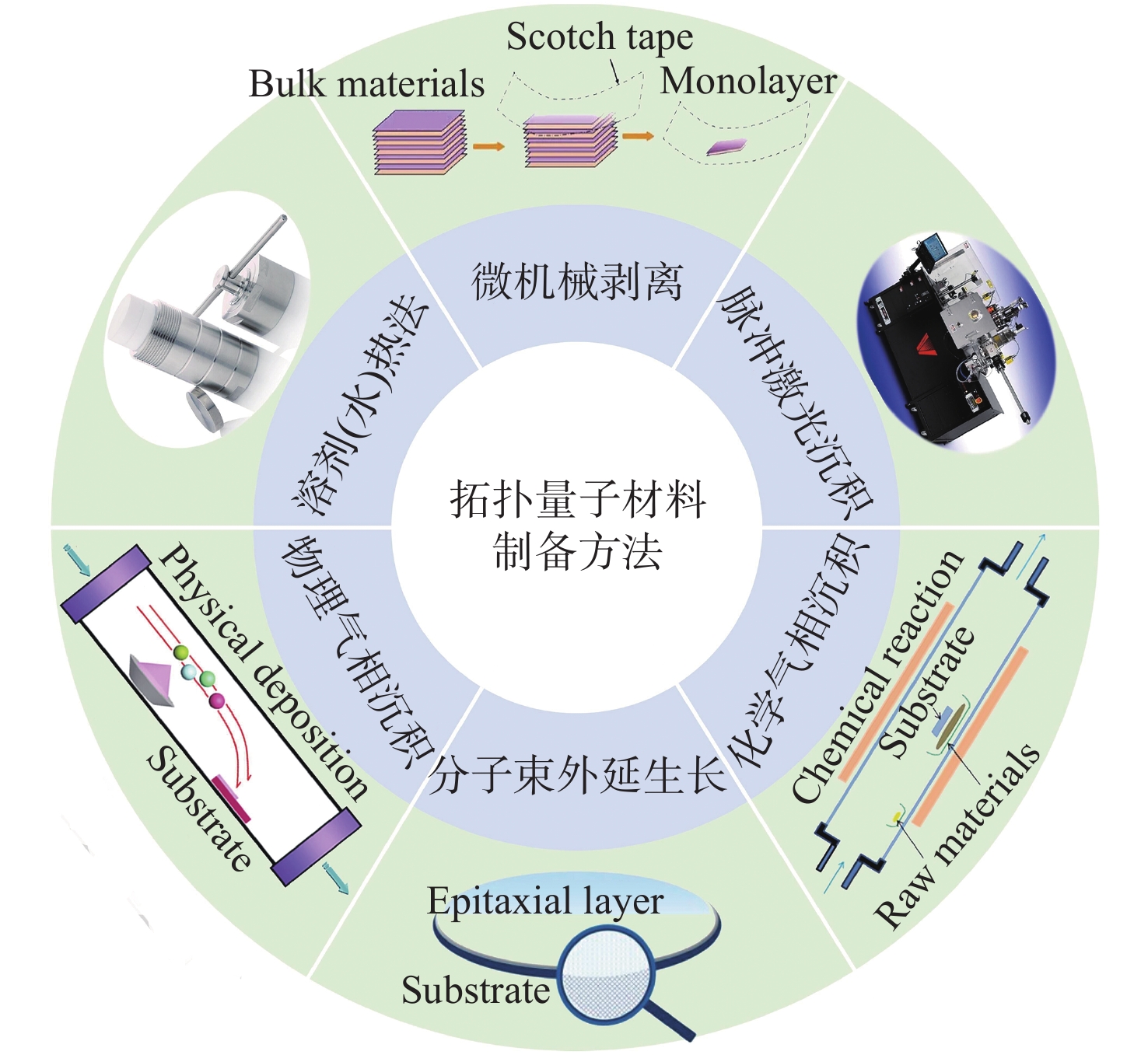
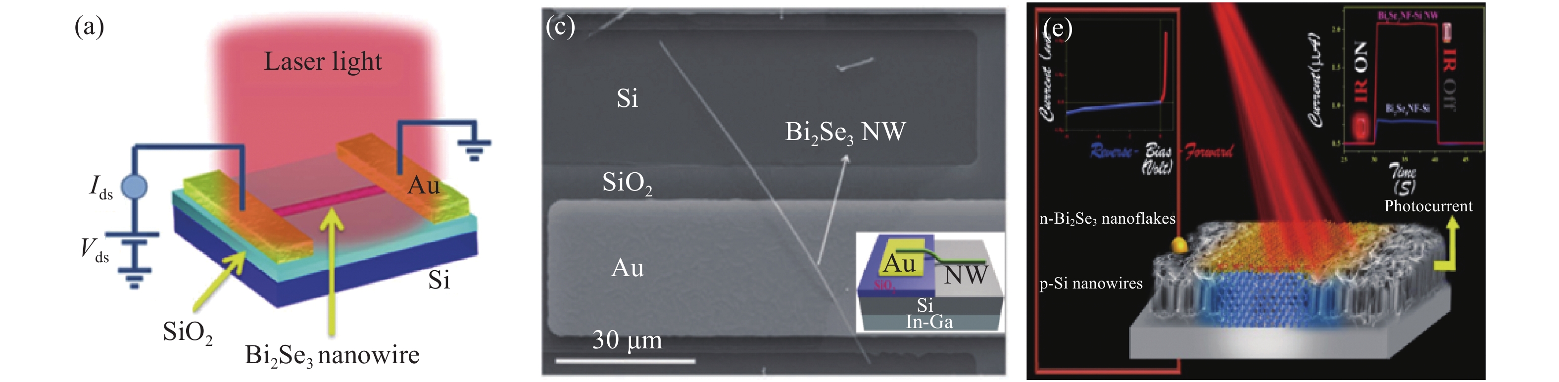
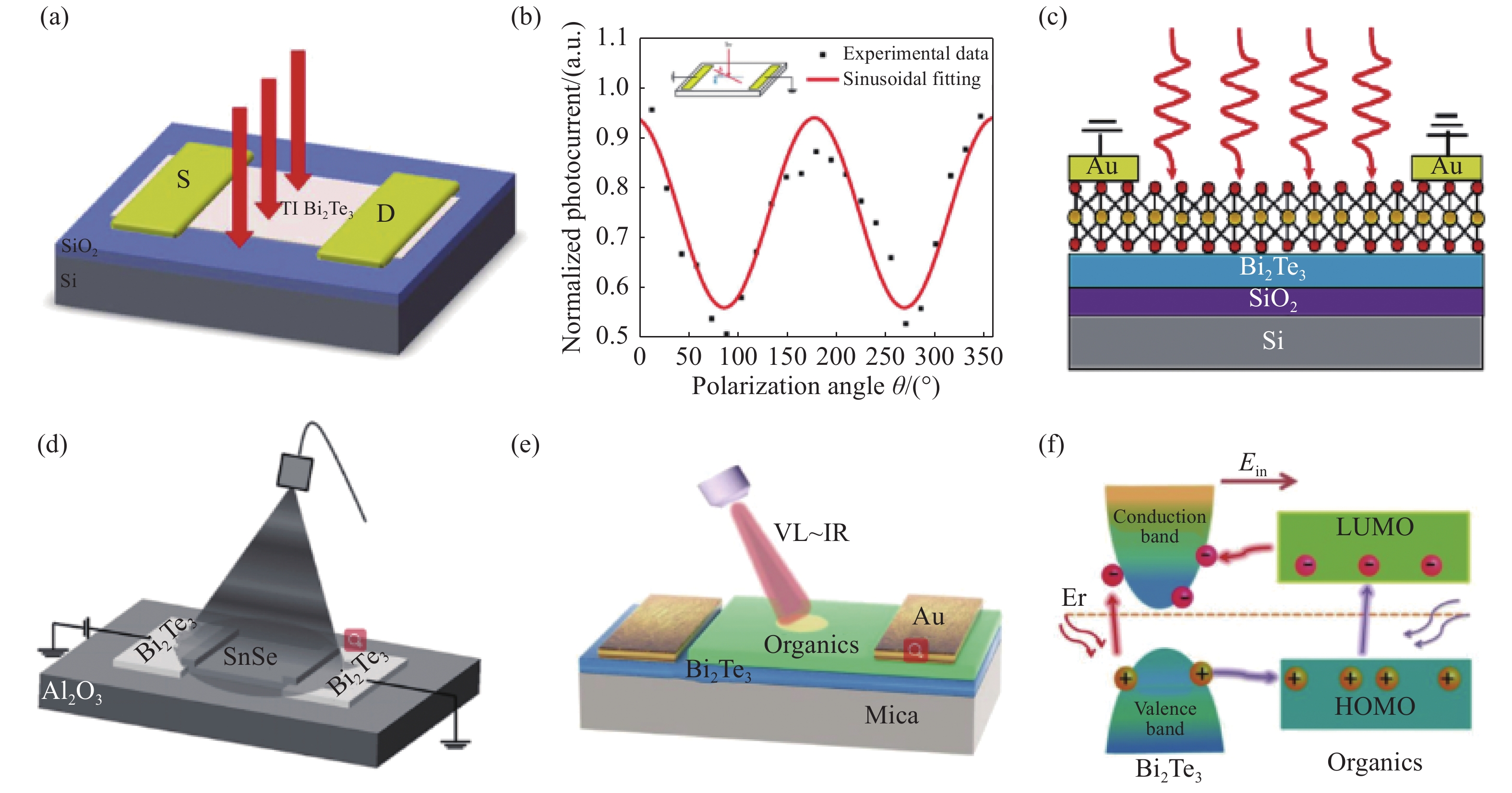
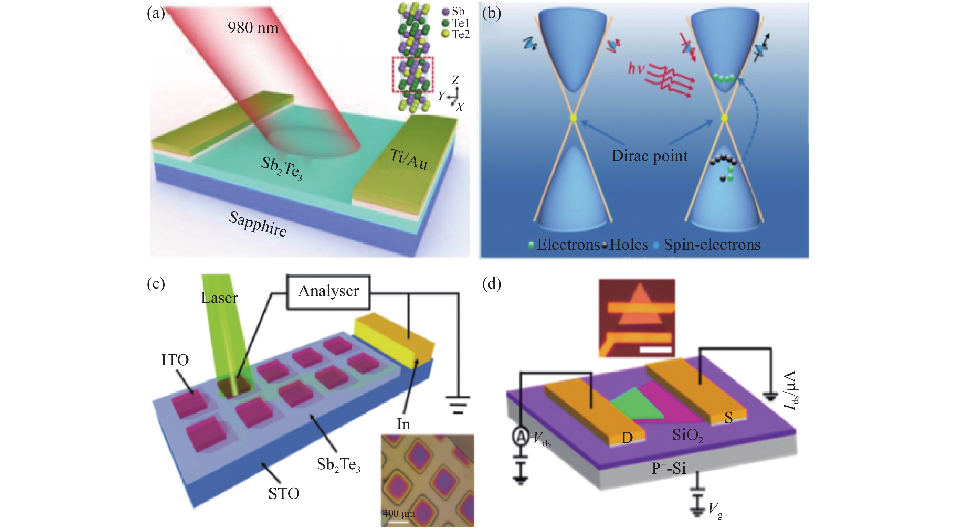
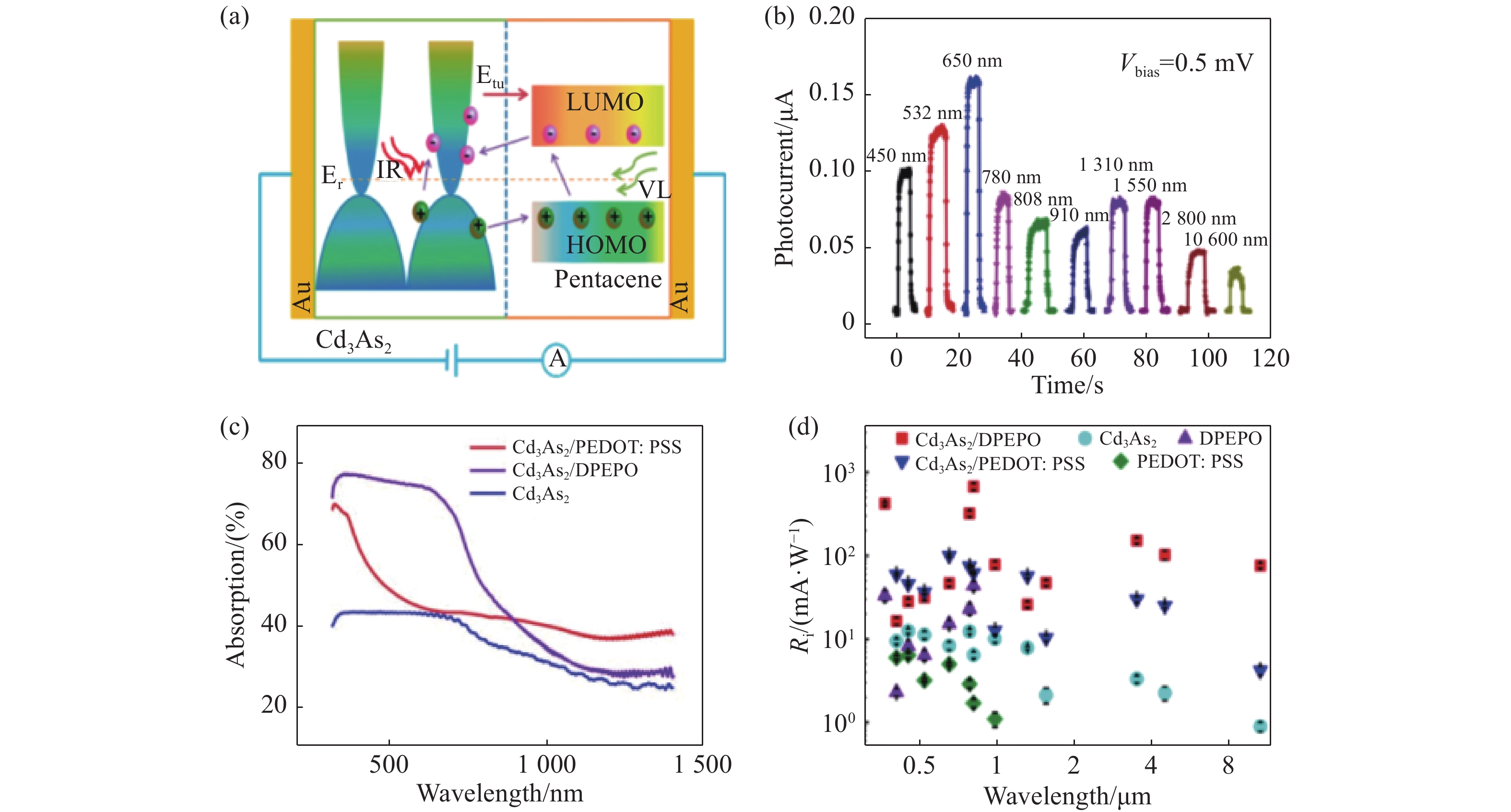
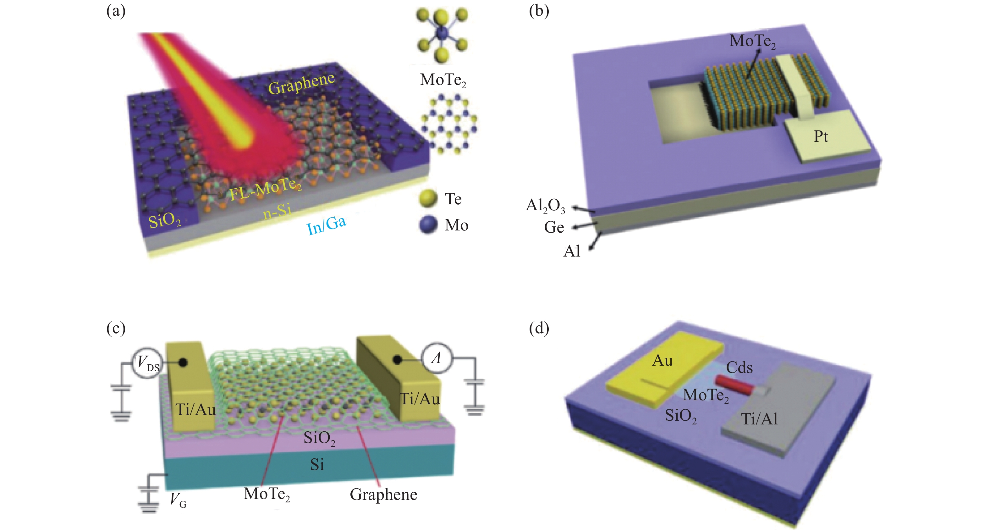
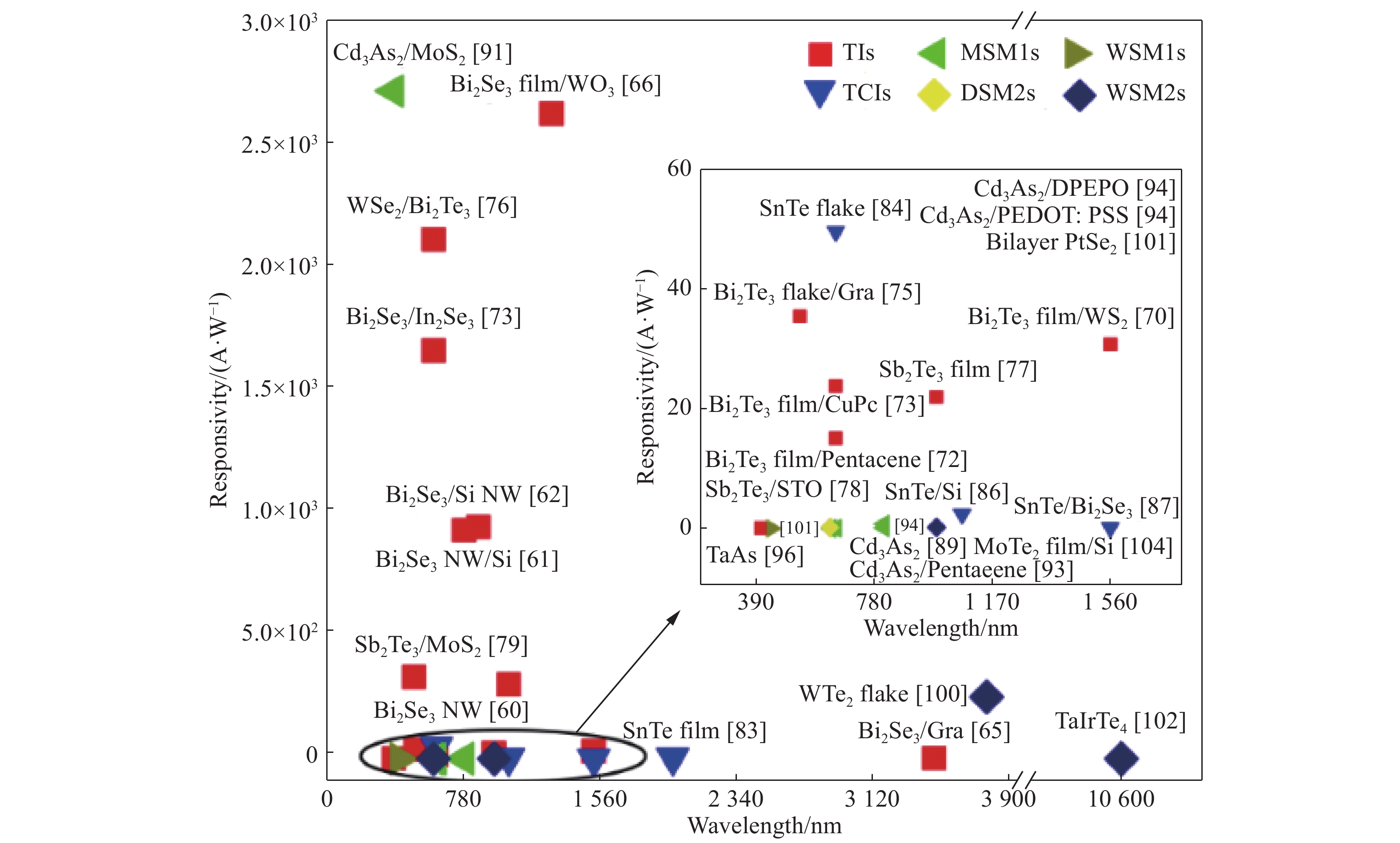
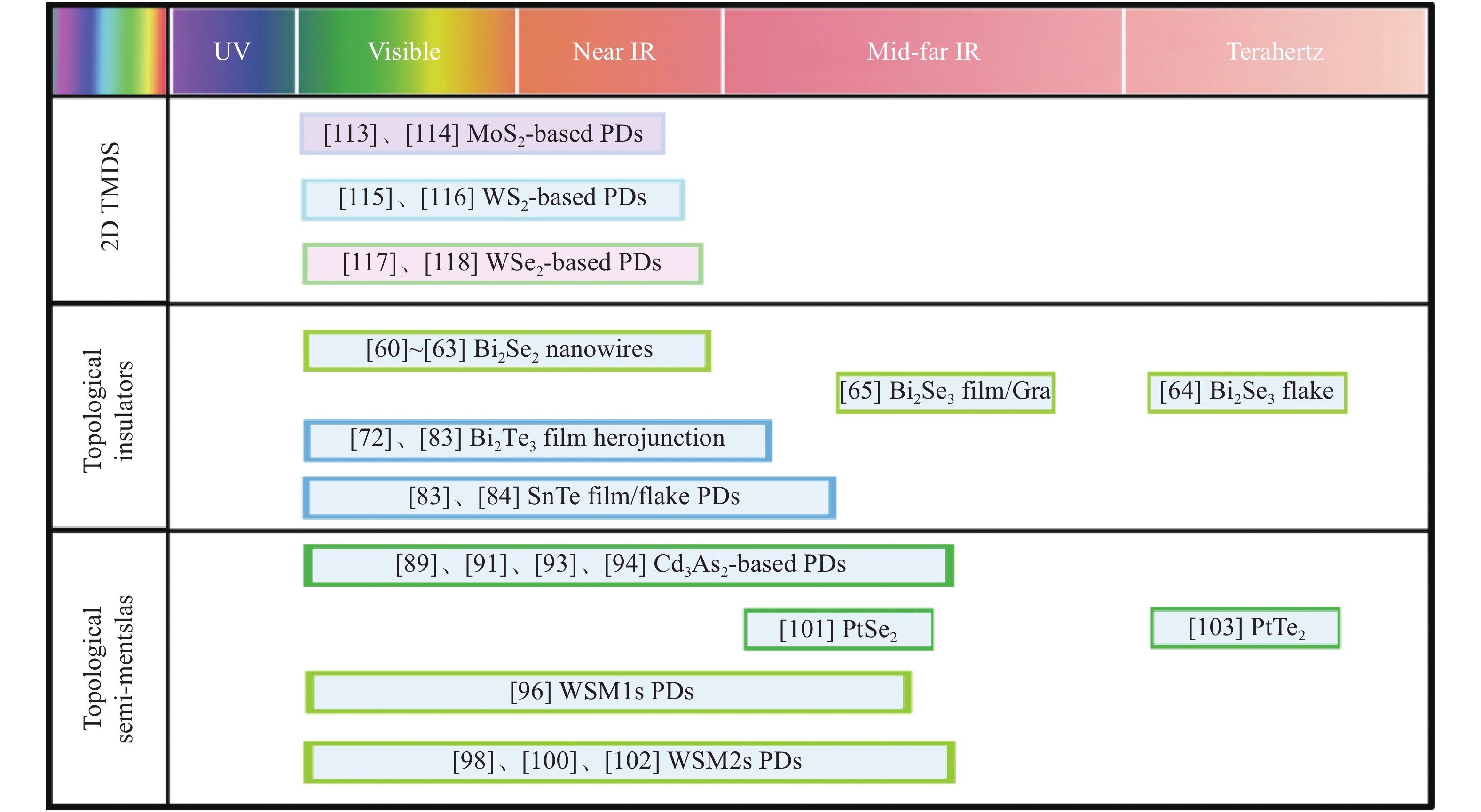
The discovery of the topological quantum states of matter is a major milestone in condensed matter physics and material science. Due to the existence of special surface states (e.g. Dirac fermions, Weyl fermions, Majorana fermions), topological quantum materials can usually exhibit some novel physical properties (such as the quantum anomalous Hall effect, 3D quantum Hall effect, Zero-band gap caused by topological states, ultra-high carrier mobility, etc.), which are different from conventional semiconductors. Because of this, there is an abundance of prospects for applications in low-power electronic and optoelectronic devices, especially in broad-spectrum detection. However, the application of topological quantum materials in the field of photoelectric detection is still in the exploratory stage at present. This article reviews the characteristics and preparation methods of topological quantum materials and the development status with respect to optical-sensing materials in photodetectors. The structure and performance of the devices based on topological quantum materials are also mentioned as the development prospects in the field of broad-spectrum detection.
The discovery of the topological quantum states of matter is a major milestone in condensed matter physics and material science. Due to the existence of special surface states (e.g. Dirac fermions, Weyl fermions, Majorana fermions), topological quantum materials can usually exhibit some novel physical properties (such as the quantum anomalous Hall effect, 3D quantum Hall effect, Zero-band gap caused by topological states, ultra-high carrier mobility, etc.), which are different from conventional semiconductors. Because of this, there is an abundance of prospects for applications in low-power electronic and optoelectronic devices, especially in broad-spectrum detection. However, the application of topological quantum materials in the field of photoelectric detection is still in the exploratory stage at present. This article reviews the characteristics and preparation methods of topological quantum materials and the development status with respect to optical-sensing materials in photodetectors. The structure and performance of the devices based on topological quantum materials are also mentioned as the development prospects in the field of broad-spectrum detection.


2021, 14(1): 66-76.
doi: 10.37188/CO.2020-0192
cstr: 32171.14.CO.2020-0192
Abstract:
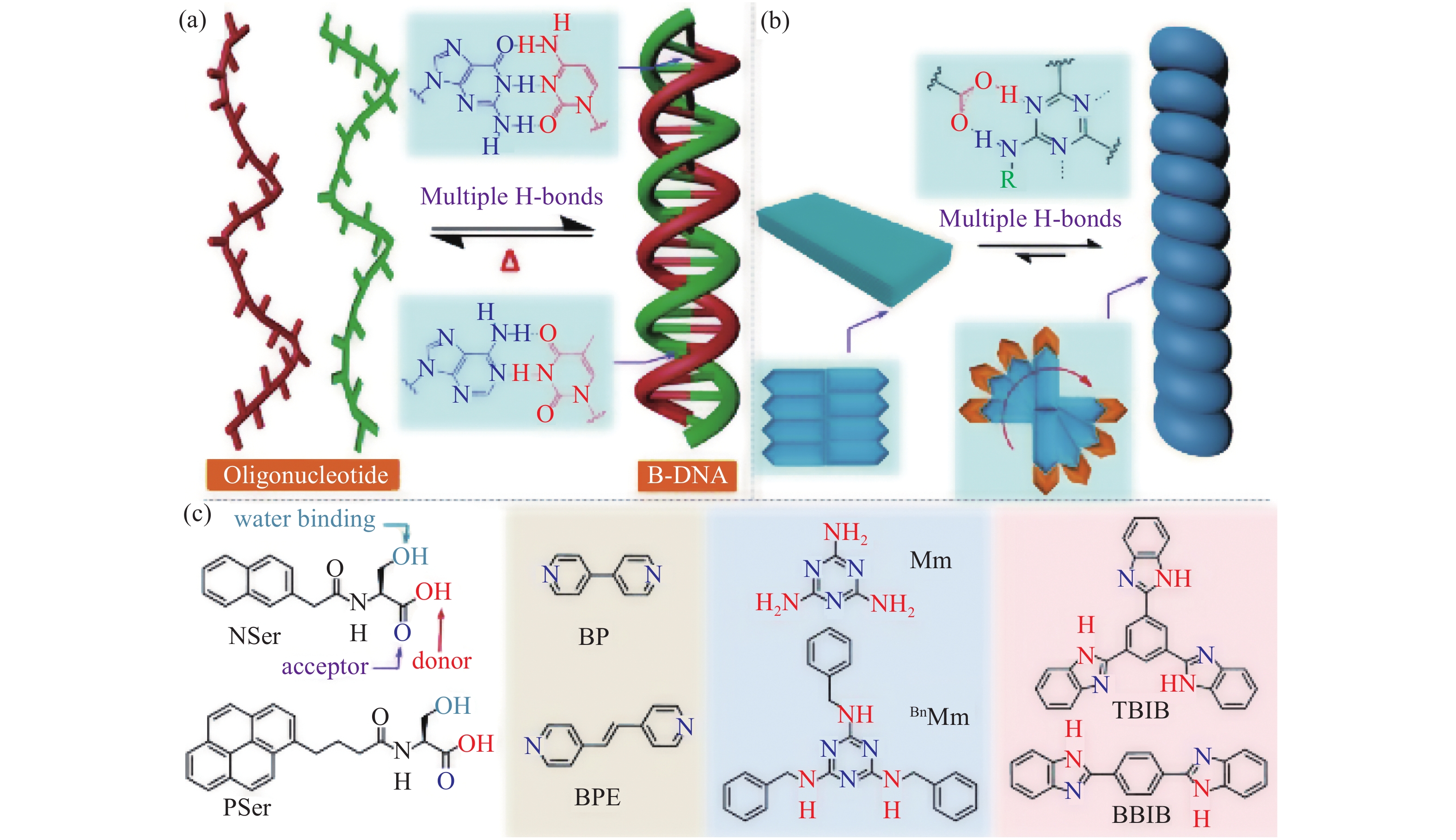
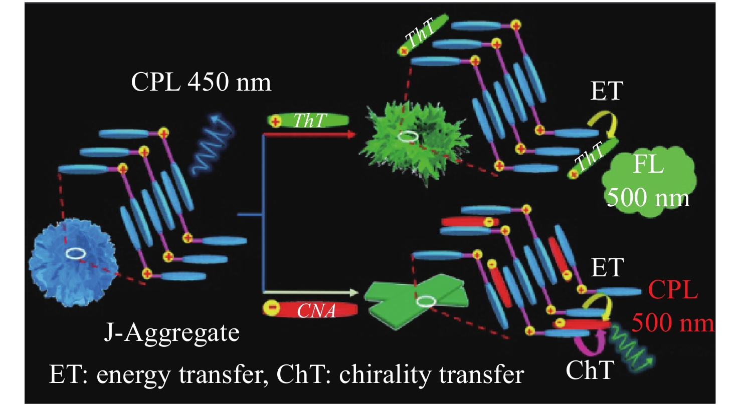
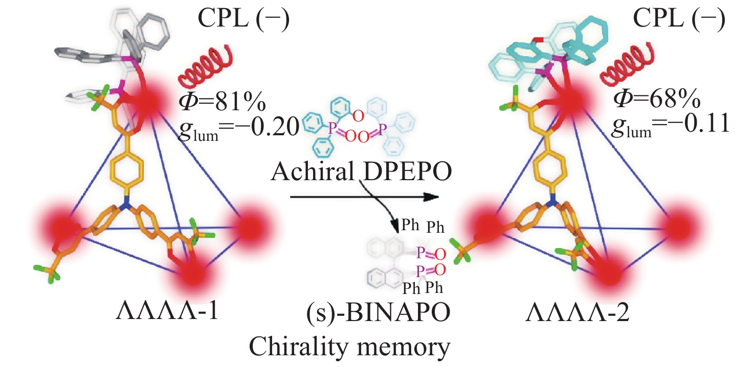
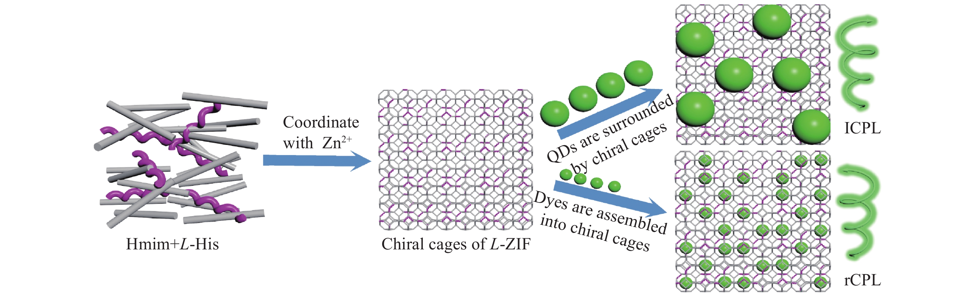
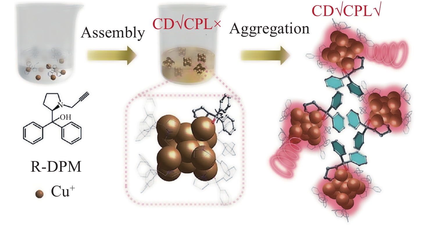
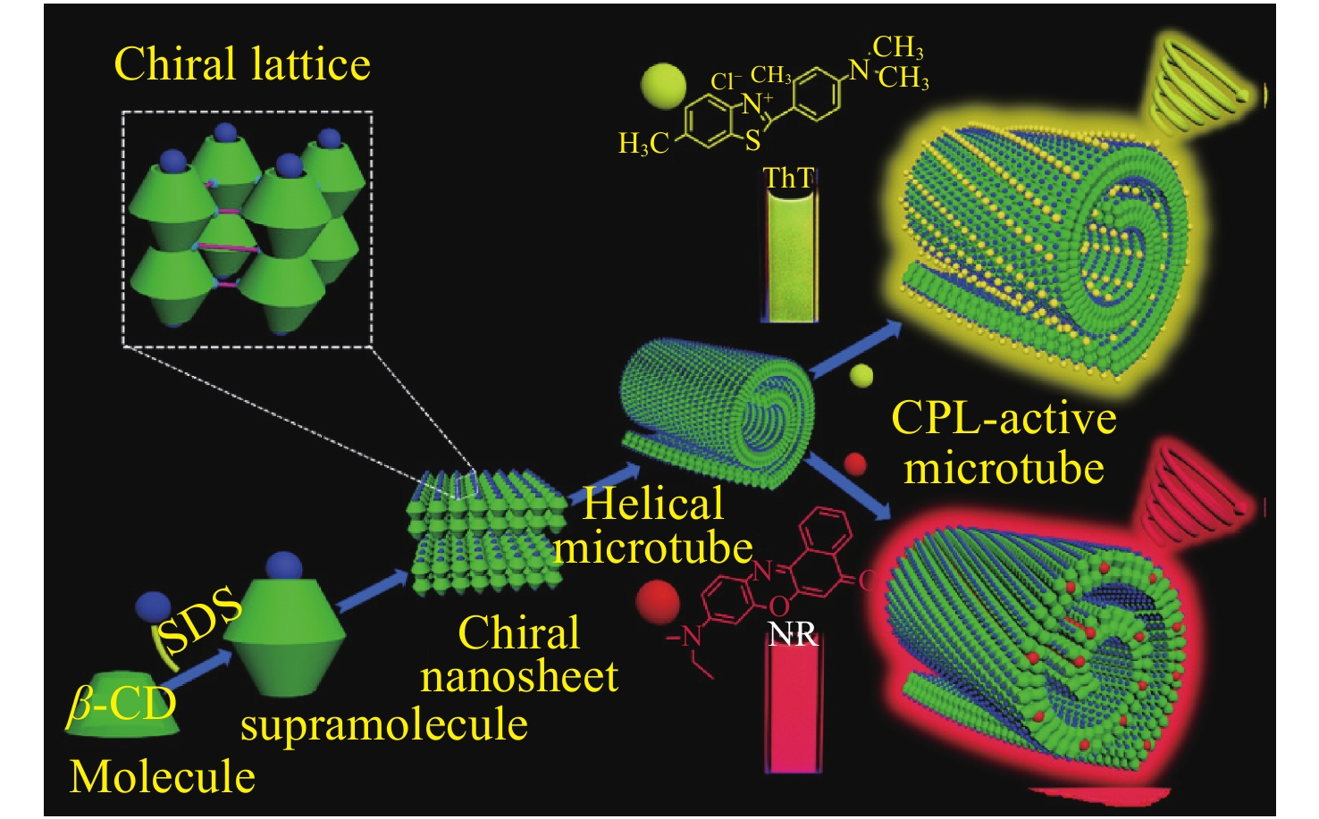
In recent years, materials with Circularly Polarized Luminescence (CPL) have received growing attention due to their wide applications in 3D displays, optical storage, optical security, etc. Supramolecular self-assembling is one of the most effective methods to construct CPL active materials, which can assemble different types of molecules into low-dimensional (0D, 1D and 2D) structures with unique functions. This review summarizes the research progress of self-assembled CPL active organic low-dimensional materials from recent years with emphasis on the driving force of supramolecular self-assembly. Firstly, the review systematically summarizes the current design strategies of self-assembled CPL active organic low-dimensional materials. Secondly, it focuses on their performance and applications. Finally, it discusses the future opportunities and challenges of this rapidly developing field.
In recent years, materials with Circularly Polarized Luminescence (CPL) have received growing attention due to their wide applications in 3D displays, optical storage, optical security, etc. Supramolecular self-assembling is one of the most effective methods to construct CPL active materials, which can assemble different types of molecules into low-dimensional (0D, 1D and 2D) structures with unique functions. This review summarizes the research progress of self-assembled CPL active organic low-dimensional materials from recent years with emphasis on the driving force of supramolecular self-assembly. Firstly, the review systematically summarizes the current design strategies of self-assembled CPL active organic low-dimensional materials. Secondly, it focuses on their performance and applications. Finally, it discusses the future opportunities and challenges of this rapidly developing field.


2021, 14(1): 77-86.
doi: 10.37188/CO.2020-0060
cstr: 32171.14.CO.2020-0060
Abstract:
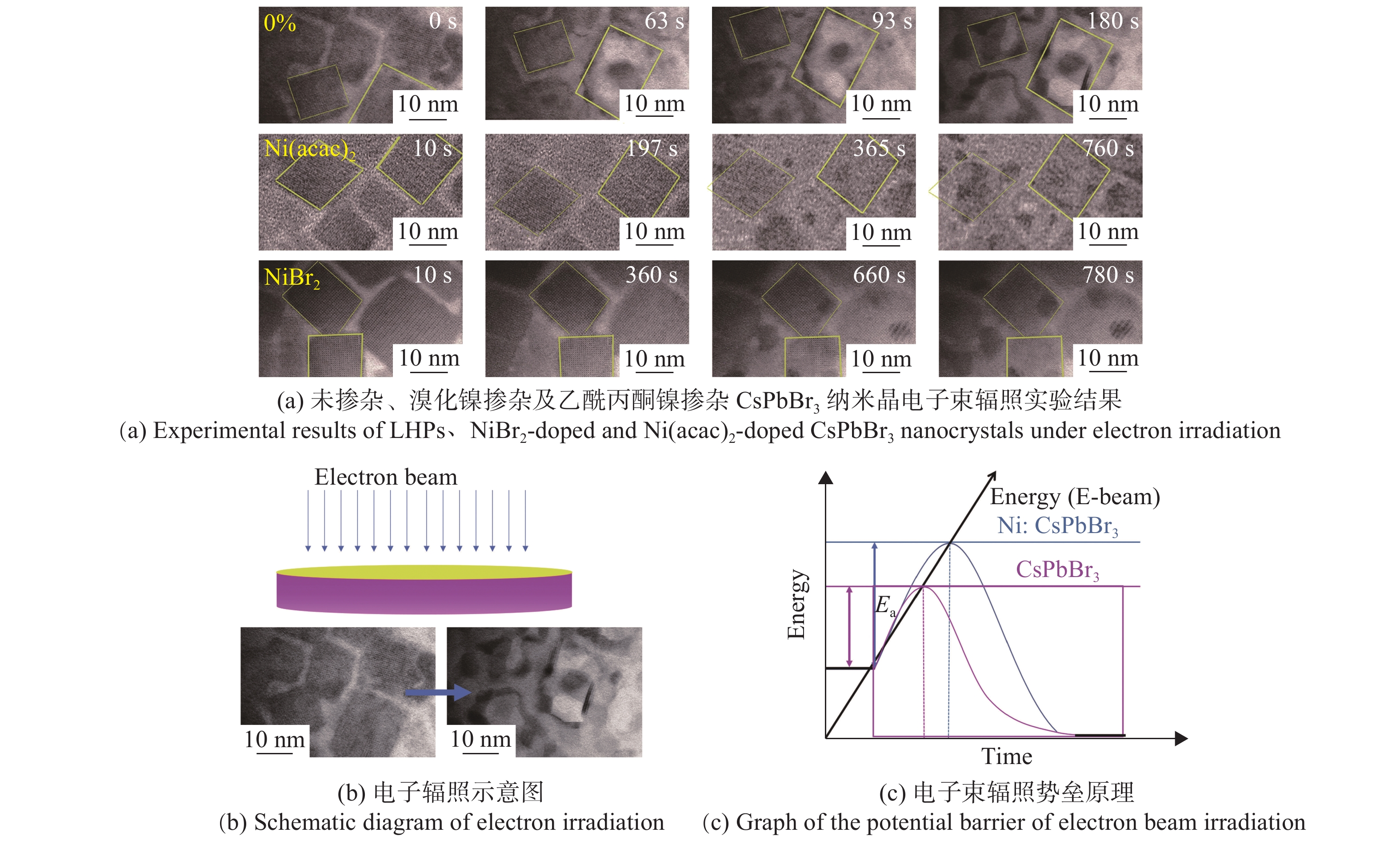
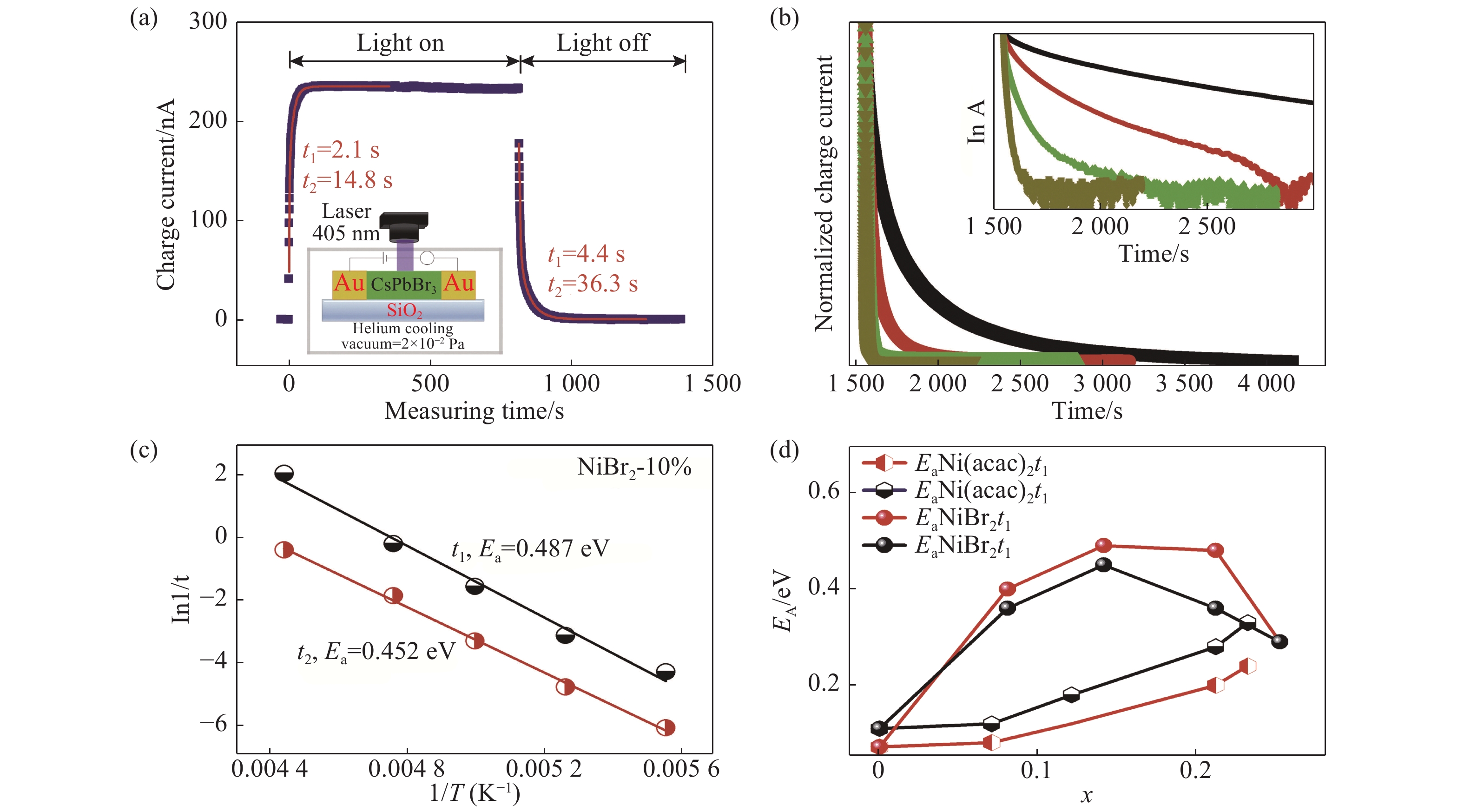
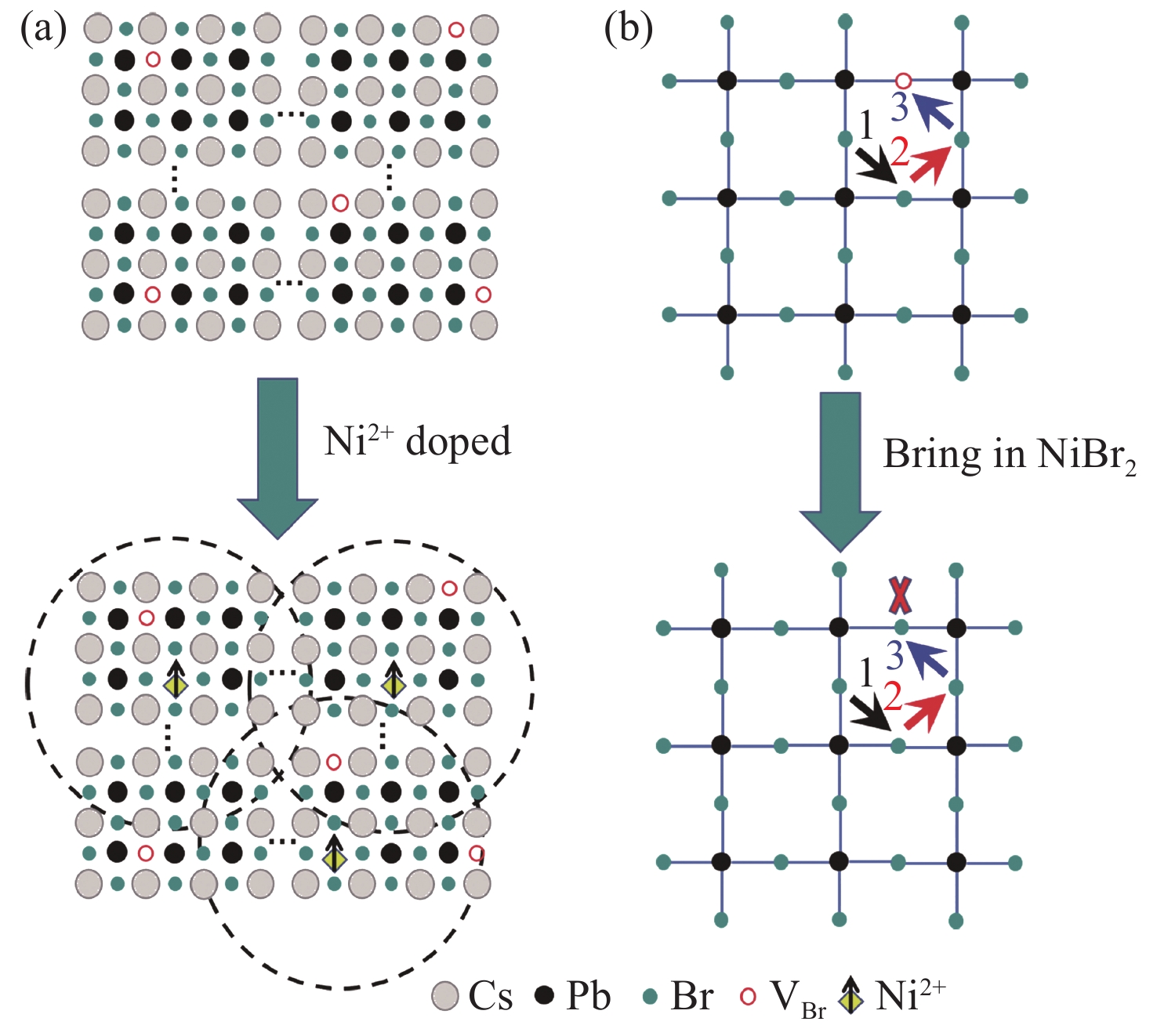
Lead Halide Perovskites(LHPs) are promising candidates for next-generation optoelectronic application. However, defect-induced ion migration causes phase degradation in LHP nanocrystals. Therefore, material stability has become an urgent problem that impedes practical applications. In this paper, we aim to study the influence of doping cations on inhibiting the migration of halogen ions in perovskite nanocrystals. Through the measurement of ion migration activation energy and in-situ high-resolution transmission electron microscope technology, the effect of precursor dopants on the stability of LHPs were analyzed. Firstly, we synthesized two types of LHP nanocrystals with high crystal quality using nickel acetylacetonate and nickel bromide as precursor dopants, respectively. Secondly, the optical properties and component elements of the doped samples were analyzed by absorption-fluorescence spectroscopy, X-ray diffraction, X-ray photoelectron diffraction, and transmission electron microscopy. Finally, the ion migration activation energies of various LHP films were measured using temperature-dependent ion conductivity tests, and the influence of the precursor dopants on the stability of as-synthesized doped LHPs was compared with the results from high-resolution electron microscopy. The results showed that the activation energies of the doped CsPbBr3 samples were significantly improved compared to the intrinsic CsPbBr3 sample (0.07 eV), which were determined to be 0.238 eV for nickel acetylacetonate and 0.487 eV for nickel bromide. In addition, the electron irradiation experiments showed that the nickel bromide-doped perovskite nanocrystals exhibited higher structural stability. This is due to the strong bonding of doped Ni2+ to halogen and the synergistic passivation effect of halogen filling vacancy defects. It can be concluded that Ni2+ doping and halogen vacancy filling can effectively inhibit ion migration in halide perovskite nanocrystals.
Lead Halide Perovskites(LHPs) are promising candidates for next-generation optoelectronic application. However, defect-induced ion migration causes phase degradation in LHP nanocrystals. Therefore, material stability has become an urgent problem that impedes practical applications. In this paper, we aim to study the influence of doping cations on inhibiting the migration of halogen ions in perovskite nanocrystals. Through the measurement of ion migration activation energy and in-situ high-resolution transmission electron microscope technology, the effect of precursor dopants on the stability of LHPs were analyzed. Firstly, we synthesized two types of LHP nanocrystals with high crystal quality using nickel acetylacetonate and nickel bromide as precursor dopants, respectively. Secondly, the optical properties and component elements of the doped samples were analyzed by absorption-fluorescence spectroscopy, X-ray diffraction, X-ray photoelectron diffraction, and transmission electron microscopy. Finally, the ion migration activation energies of various LHP films were measured using temperature-dependent ion conductivity tests, and the influence of the precursor dopants on the stability of as-synthesized doped LHPs was compared with the results from high-resolution electron microscopy. The results showed that the activation energies of the doped CsPbBr3 samples were significantly improved compared to the intrinsic CsPbBr3 sample (0.07 eV), which were determined to be 0.238 eV for nickel acetylacetonate and 0.487 eV for nickel bromide. In addition, the electron irradiation experiments showed that the nickel bromide-doped perovskite nanocrystals exhibited higher structural stability. This is due to the strong bonding of doped Ni2+ to halogen and the synergistic passivation effect of halogen filling vacancy defects. It can be concluded that Ni2+ doping and halogen vacancy filling can effectively inhibit ion migration in halide perovskite nanocrystals.
2021, 14(1): 87-99.
doi: 10.37188/CO.2020-0139
cstr: 32171.14.CO.2020-0139
Abstract:
To achieve weak signal detection, high sensitivity is required. Because of their strengths in optical and electrical properties such as wide spectral absorption, adjustable bandgap, and high carrier mobility, graphene, Transition Metal dichalcogenides (TMDs), Black Phosphorus (BP) and other two-dimensional (2D) materials have been used to fabricate infrared detectors. However, those 2D materials have disadvantages of weak light absorption, low carrier mobility and air instability, that restrict their applications in high-sensitivity infrared detection. Compared with single two-dimensional material, heterostructures consisting of two or more single 2D materials adopt the characteristics of each single material as well as some novel physical properties from heterojunctions/interfaces. In recent years, the heterostructure of 2D materials has been studied extensively in the field of high-sensitivity infrared detection. To gain a deep understanding of the factors affecting sensitivity, we provide a comprehensive review of the strategies that improve the sensitivity of infrared detectors and the development of high-sensitivity infrared detectors based on 2D heterojunctions in recent years. We summarize the figures of merit of these infrared detectors and identify the existing challenges impeding further improvements in sensitivity. Finally, by summarizing the challenges of future improving the sensitivity of infrared detection prospects for strategies to obtain high-sensitivity infrared detectors with good comprehensive performance and commercial applicability are presented with considerations for balancing the detector’s responsivity and response speed, large area two-dimensional heterojunction preparation, heterojunction interface optimization, and so forth.
To achieve weak signal detection, high sensitivity is required. Because of their strengths in optical and electrical properties such as wide spectral absorption, adjustable bandgap, and high carrier mobility, graphene, Transition Metal dichalcogenides (TMDs), Black Phosphorus (BP) and other two-dimensional (2D) materials have been used to fabricate infrared detectors. However, those 2D materials have disadvantages of weak light absorption, low carrier mobility and air instability, that restrict their applications in high-sensitivity infrared detection. Compared with single two-dimensional material, heterostructures consisting of two or more single 2D materials adopt the characteristics of each single material as well as some novel physical properties from heterojunctions/interfaces. In recent years, the heterostructure of 2D materials has been studied extensively in the field of high-sensitivity infrared detection. To gain a deep understanding of the factors affecting sensitivity, we provide a comprehensive review of the strategies that improve the sensitivity of infrared detectors and the development of high-sensitivity infrared detectors based on 2D heterojunctions in recent years. We summarize the figures of merit of these infrared detectors and identify the existing challenges impeding further improvements in sensitivity. Finally, by summarizing the challenges of future improving the sensitivity of infrared detection prospects for strategies to obtain high-sensitivity infrared detectors with good comprehensive performance and commercial applicability are presented with considerations for balancing the detector’s responsivity and response speed, large area two-dimensional heterojunction preparation, heterojunction interface optimization, and so forth.

2021, 14(1): 100-116.
doi: 10.37188/CO.2020-0082
cstr: 32171.14.CO.2020-0082
Abstract:
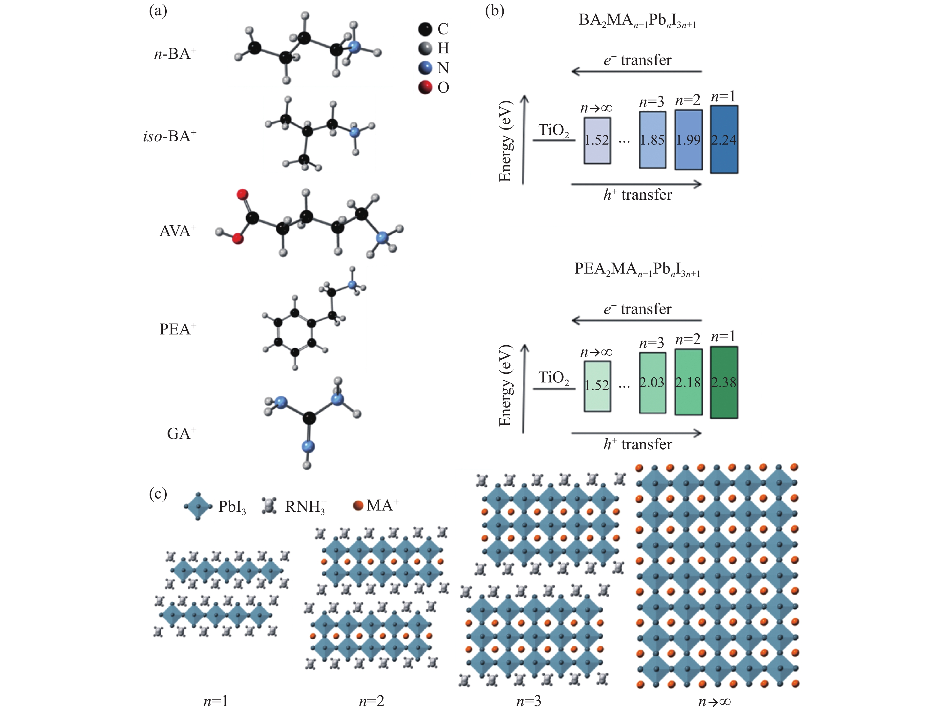
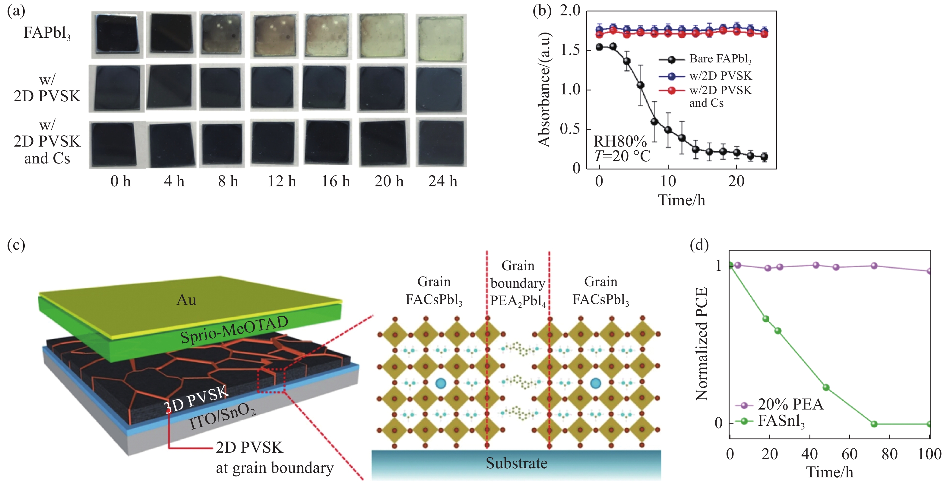
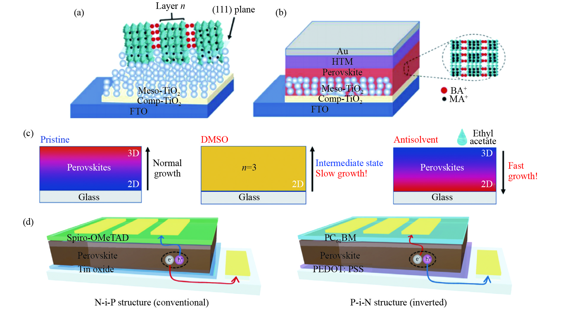
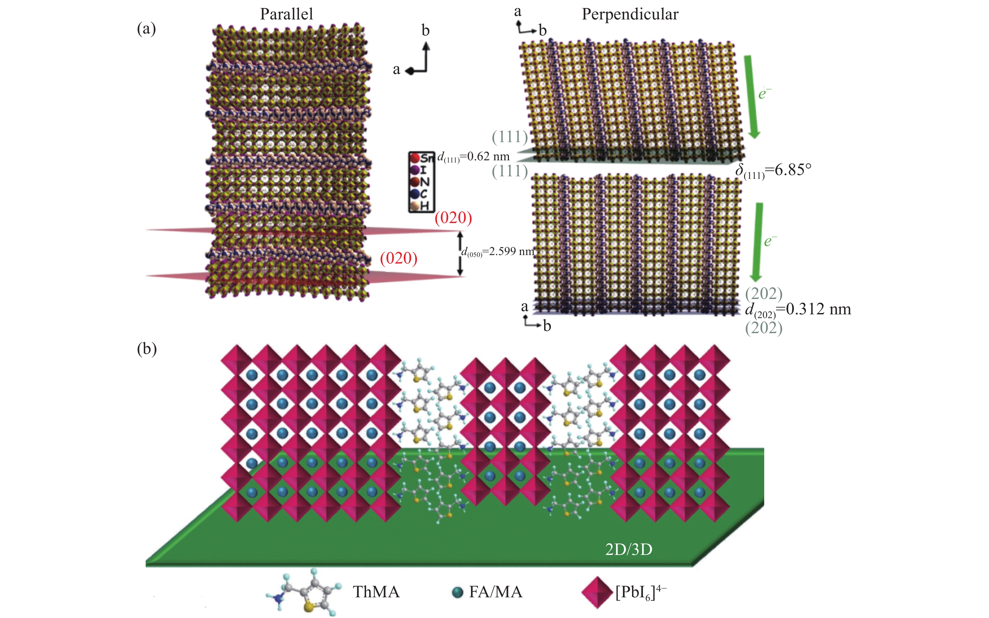
At present, the power conversion efficiency of perovskite solar cells exceeds 25%. Their rapidly increasing efficiency has made people increasingly optimistic about their commercial application, but the stability of perovskite remains the biggest obstacle to successful commercialization. Quasi-two-dimensional perovskite solves this problem.
Utilizing the hydrophobicity and thermal stability of large organic spacer cations, quasi-two-dimensional perovskite can effectively improve the stability of perovskite and improved crystal formation energy while providing a more stable structure. Quasi-two-dimensional perovskite also invites significant improvement to the morphology of perovskite films, which can replace anti-solvent processes, simplify production, and meet the industrial production requirements of perovskite. However, the relatively large band-gap and low carrier mobility caused by insulated organic spacer cations hinder ion transmission, causing quasi-two-dimensional perovskite solar cells to be far less efficient than three-dimensional perovskite solar cells. Therefore, for quasi-two-dimensional perovskite, it is necessary to further study its characteristics and device applications to achieve further optimization of device performance.
This article summarizes the research progress of quasi-two-dimensional perovskite solar cells, the molecular structure of quasi-two-dimensional perovskite, the methods and principles of quasi-two-dimensional doping that improves the stability of three-dimensional perovskite, and the phase distribution and carrier transport characteristics of quasi-two-dimensional perovskite. Then this paper analyzes the problems faced by quasi-two-dimensional perovskite solar cells and looks forward to their prospects. It is expected that it will provide a reference for the preparation of efficient and stable quasi-two-dimensional perovskite solar cells.


2021, 14(1): 117-134.
doi: 10.37188/CO.2020-0184
cstr: 32171.14.CO.2020-0184
Abstract:
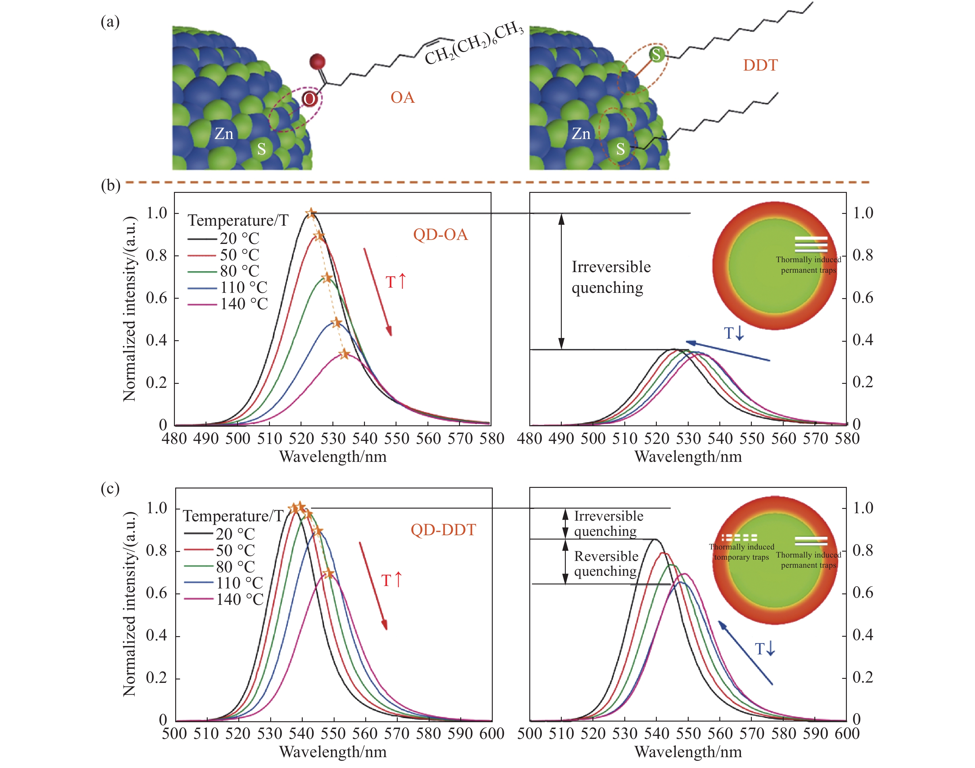
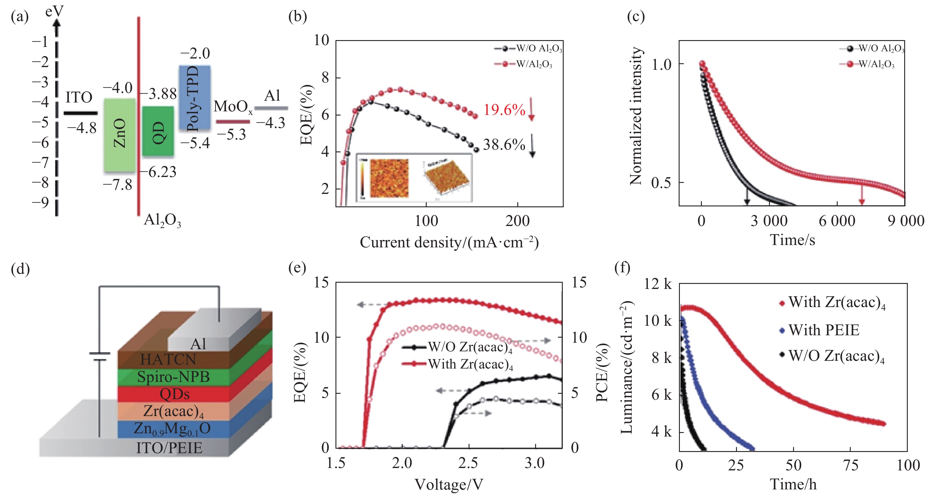
Quantum dot Light-Emitting Diodes (QLEDs) are applied to the lighting and display industry for their unique photoelectric characteristics. Their External Quantum Efficiency (EQEs) is quickly meeting commercial requirements while the device’s lifetime is still one of their biggest challenges. The significant factors affecting the lifetime of QLEDs are divided into two aspects including the stability of the functional layer’s materials and charge imbalance. Various strategies for enhancing QLEDs stability are discussed including improving the stability of quantum dots, implementing Charge Transport Layers (CTLs) and promoting charge balance. With the deepening understanding of the degradation mechanism of QLEDs, more stable quantum dots and QLEDs devices have been developed. However, there are still some obstacles to the commercialization of QLEDs. For example, the high toxicity of Cd and the lifetime and efficiency of blue QLEDs are far lower than the corresponding levels of green and red QLEDs. In addition, the stability of QLEDs at high brightness (1000 cd m−2) is usually much shorter, which still limits the development of QLEDs. Therefore, research and development efforts for QLEDs should be further strengthened to overcome these technical obstacles and achieve the future commercialization of QLEDs.
Quantum dot Light-Emitting Diodes (QLEDs) are applied to the lighting and display industry for their unique photoelectric characteristics. Their External Quantum Efficiency (EQEs) is quickly meeting commercial requirements while the device’s lifetime is still one of their biggest challenges. The significant factors affecting the lifetime of QLEDs are divided into two aspects including the stability of the functional layer’s materials and charge imbalance. Various strategies for enhancing QLEDs stability are discussed including improving the stability of quantum dots, implementing Charge Transport Layers (CTLs) and promoting charge balance. With the deepening understanding of the degradation mechanism of QLEDs, more stable quantum dots and QLEDs devices have been developed. However, there are still some obstacles to the commercialization of QLEDs. For example, the high toxicity of Cd and the lifetime and efficiency of blue QLEDs are far lower than the corresponding levels of green and red QLEDs. In addition, the stability of QLEDs at high brightness (1000 cd m−2) is usually much shorter, which still limits the development of QLEDs. Therefore, research and development efforts for QLEDs should be further strengthened to overcome these technical obstacles and achieve the future commercialization of QLEDs.


2021, 14(1): 135-144.
doi: 10.37188/CO.2020-0189
cstr: 32171.14.CO.2020-0189
Abstract:
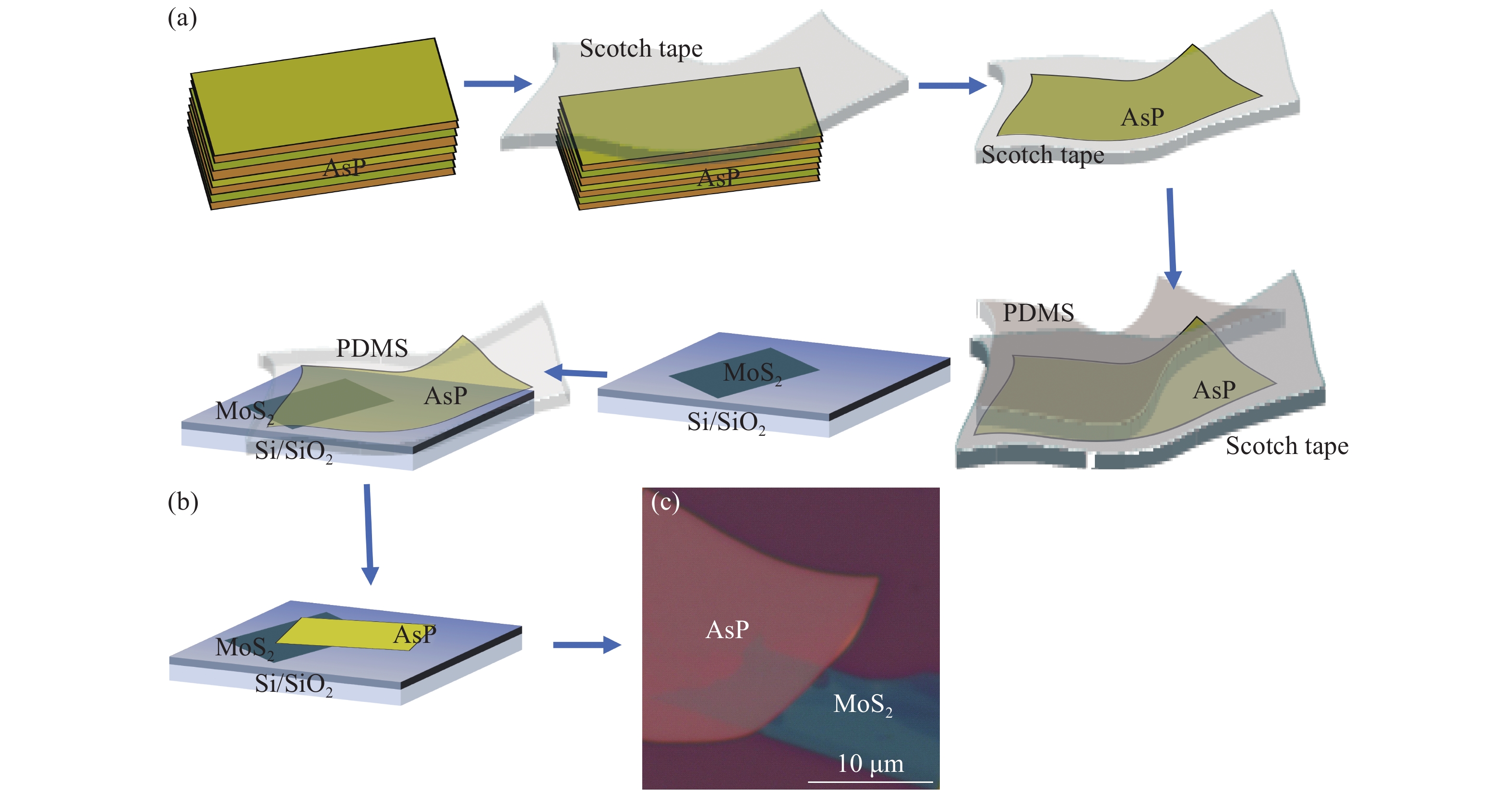
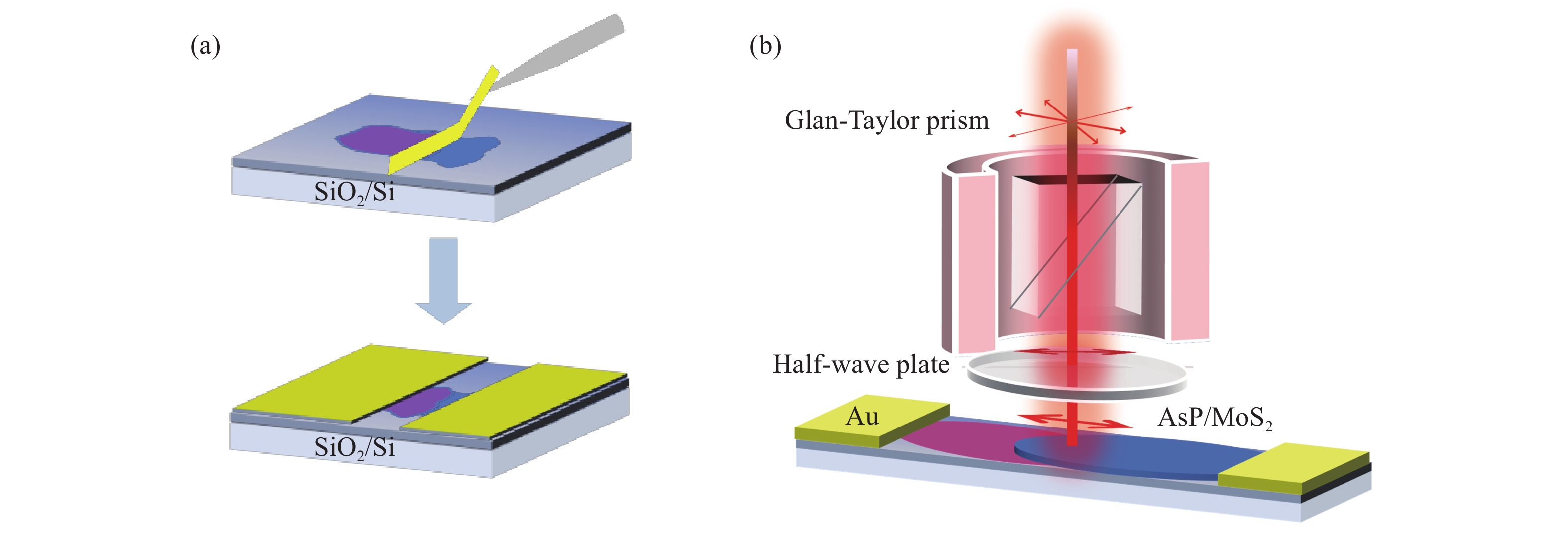
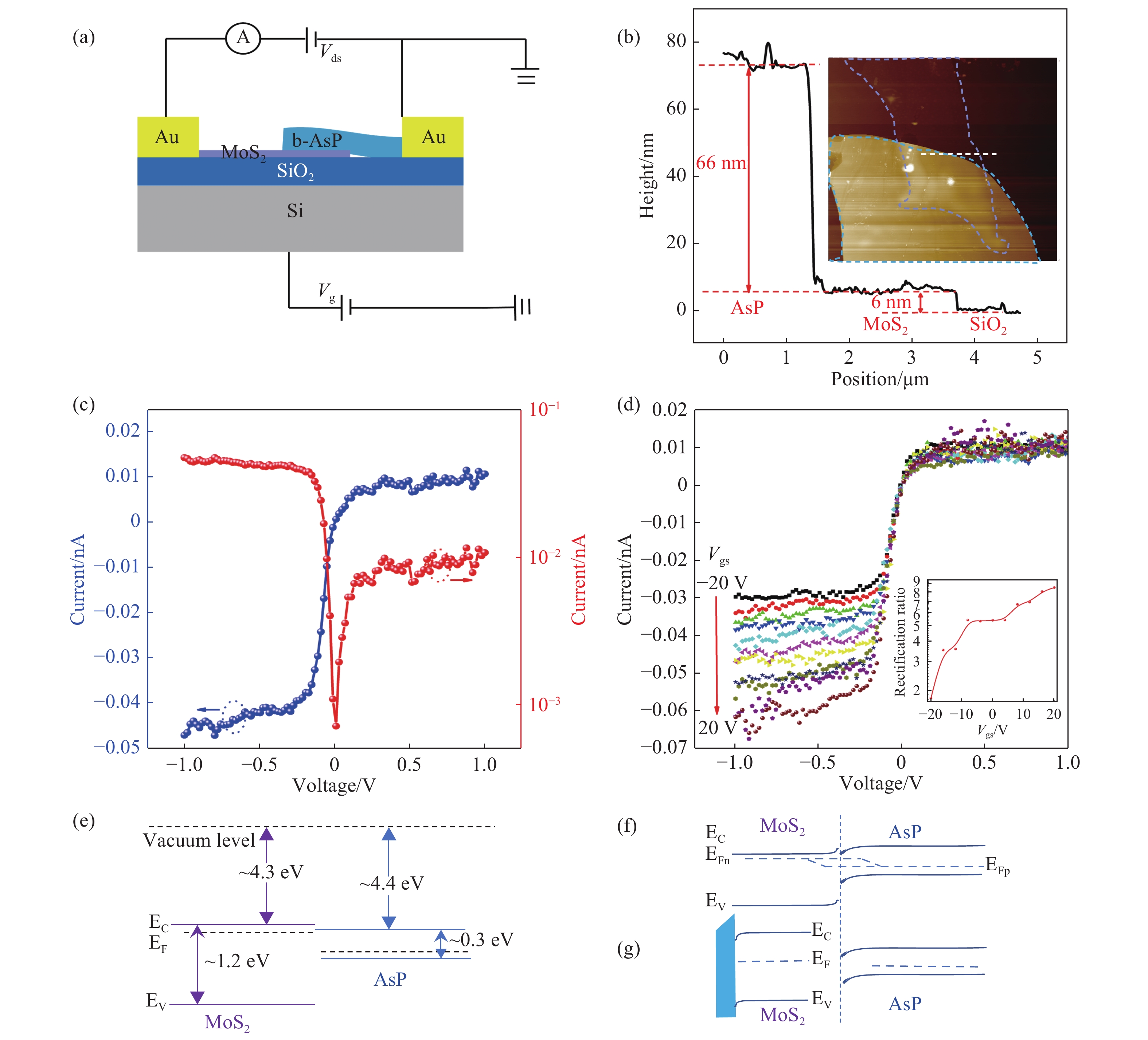
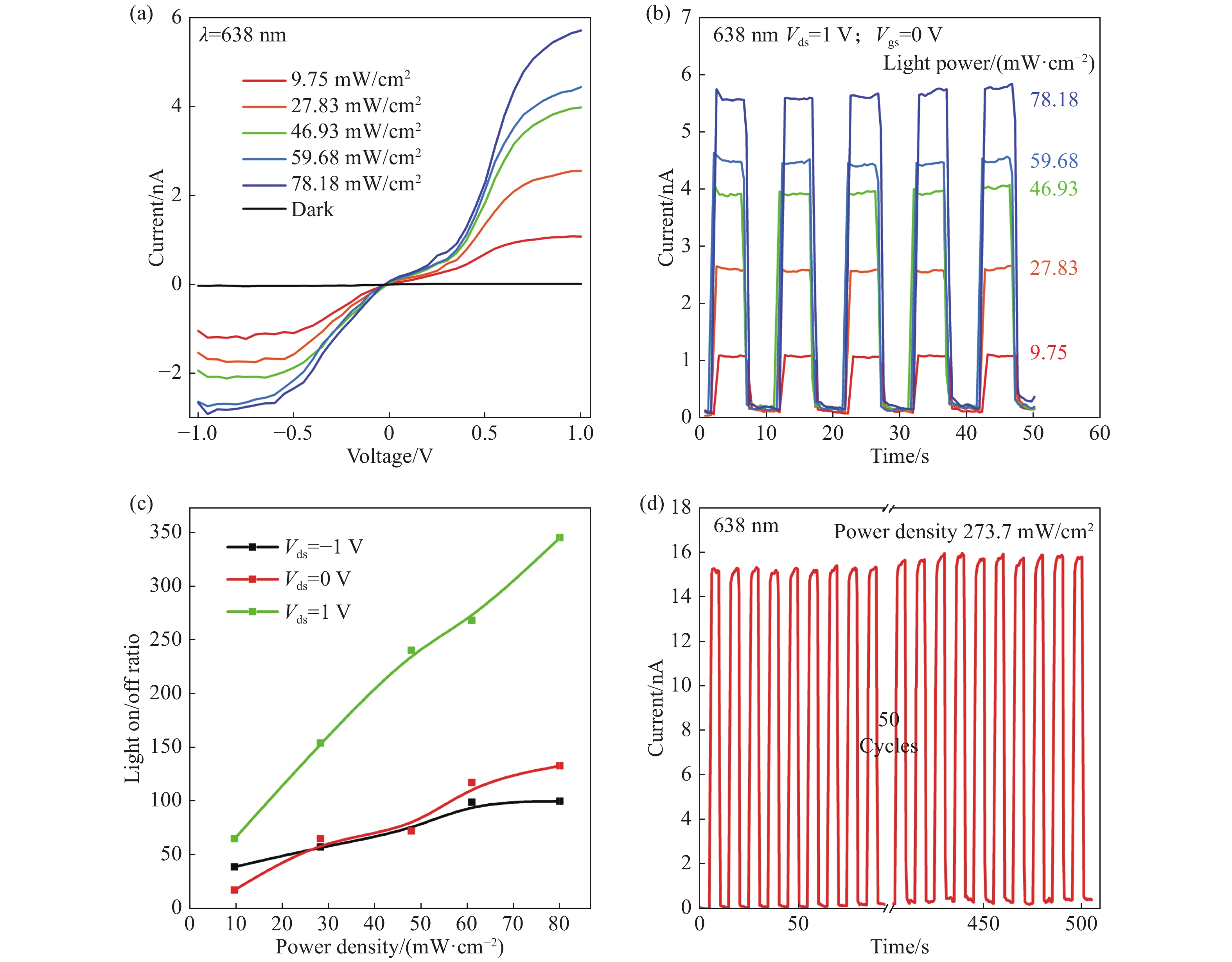
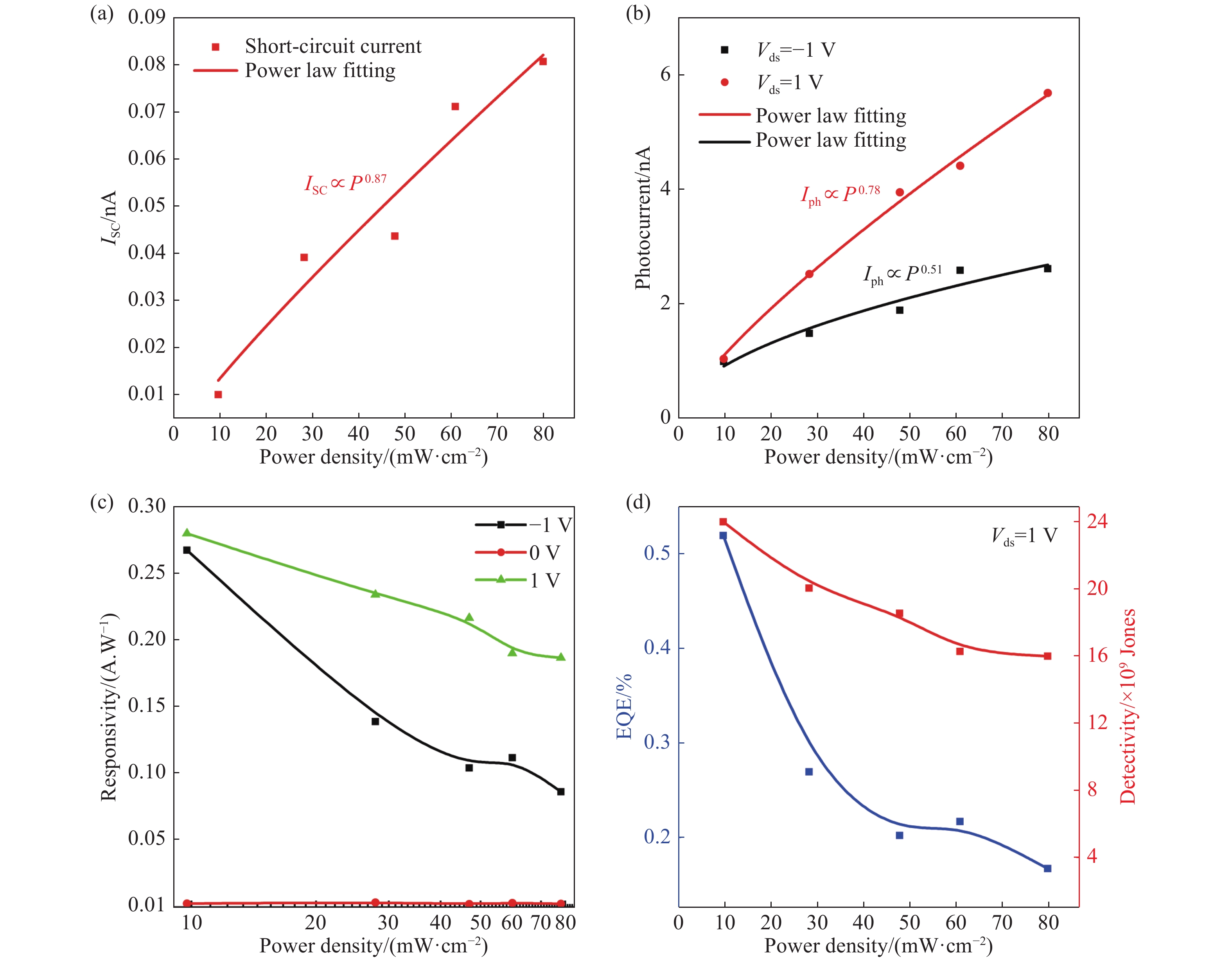
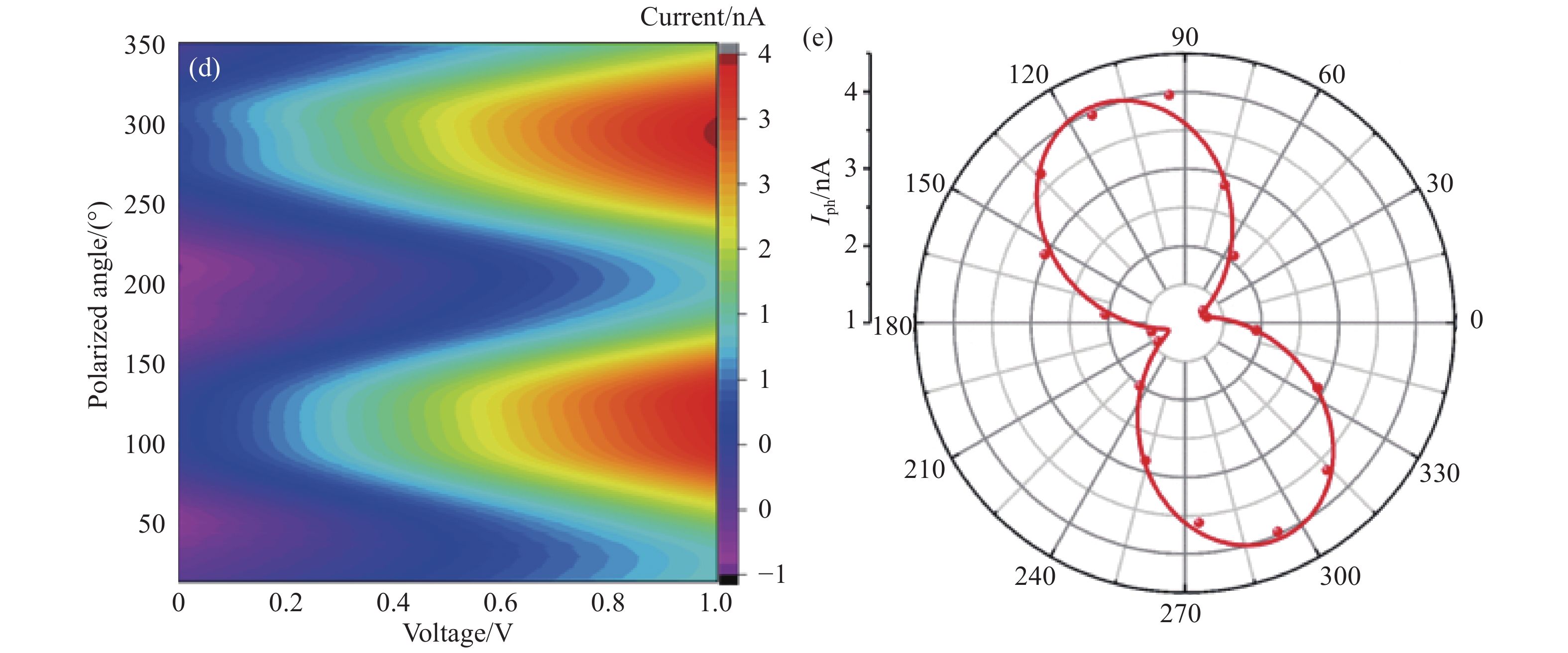
The ability to detect linearly polarized light is an important index for evaluating polarized photoelectric detectors. Black arsenic phosphorus (b-AsP) is a relatively stable anisotropic material, and is sensitive to linearly polarized light because of its anisotropy inside its planar structure. The material has important application value in polarization detection. This paper introduces a polarization-sensitive photodetector based on AsP/MoS2. Due to the anisotropic light absorption of AsP, effective carrier collection and strong carrier transport capacity of MoS2, as well as the suppression of dark current by a van der Waals heterojunction, the performance of the photodector shows relatively large on/off ratios. Moreover, the photodector has a current optical responsivity of 0.27 A/W and a detectivity of 2×10¹⁰ Jones, and more importantly, achieves a dichroic ratio of up to 3.06 at 638 nm. These experimental results show that AsP/MoS2 heterostructures have broad application prospects in the field of polarized photoelectricity detection.
The ability to detect linearly polarized light is an important index for evaluating polarized photoelectric detectors. Black arsenic phosphorus (b-AsP) is a relatively stable anisotropic material, and is sensitive to linearly polarized light because of its anisotropy inside its planar structure. The material has important application value in polarization detection. This paper introduces a polarization-sensitive photodetector based on AsP/MoS2. Due to the anisotropic light absorption of AsP, effective carrier collection and strong carrier transport capacity of MoS2, as well as the suppression of dark current by a van der Waals heterojunction, the performance of the photodector shows relatively large on/off ratios. Moreover, the photodector has a current optical responsivity of 0.27 A/W and a detectivity of 2×10¹⁰ Jones, and more importantly, achieves a dichroic ratio of up to 3.06 at 638 nm. These experimental results show that AsP/MoS2 heterostructures have broad application prospects in the field of polarized photoelectricity detection.


2021, 14(1): 145-152.
doi: 10.37188/CO.2020-0076
cstr: 32171.14.CO.2020-0076
Abstract:
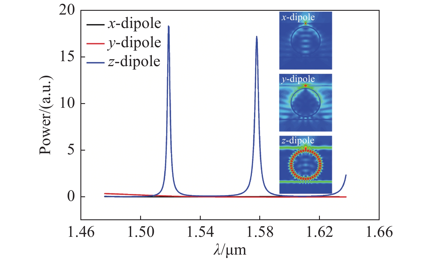
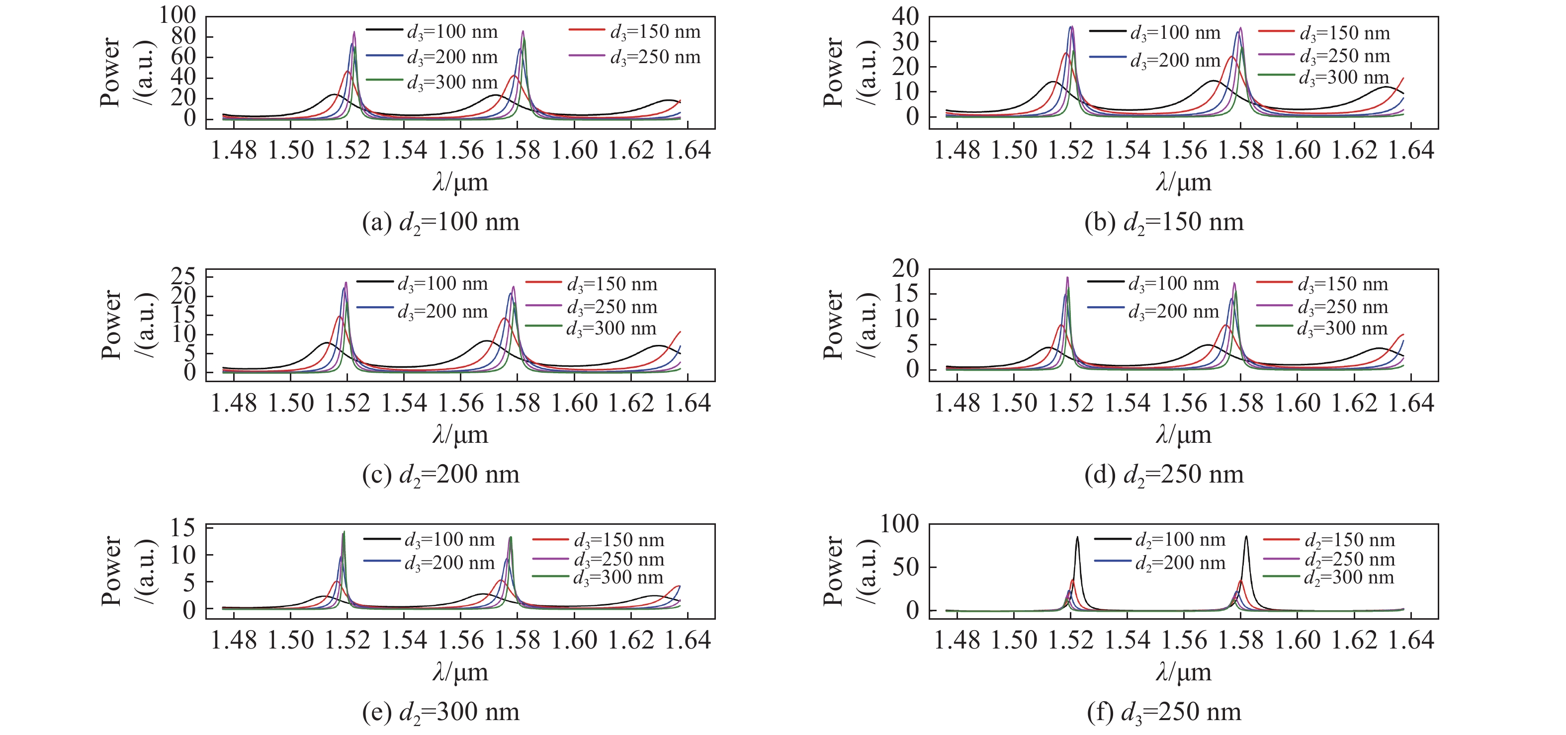
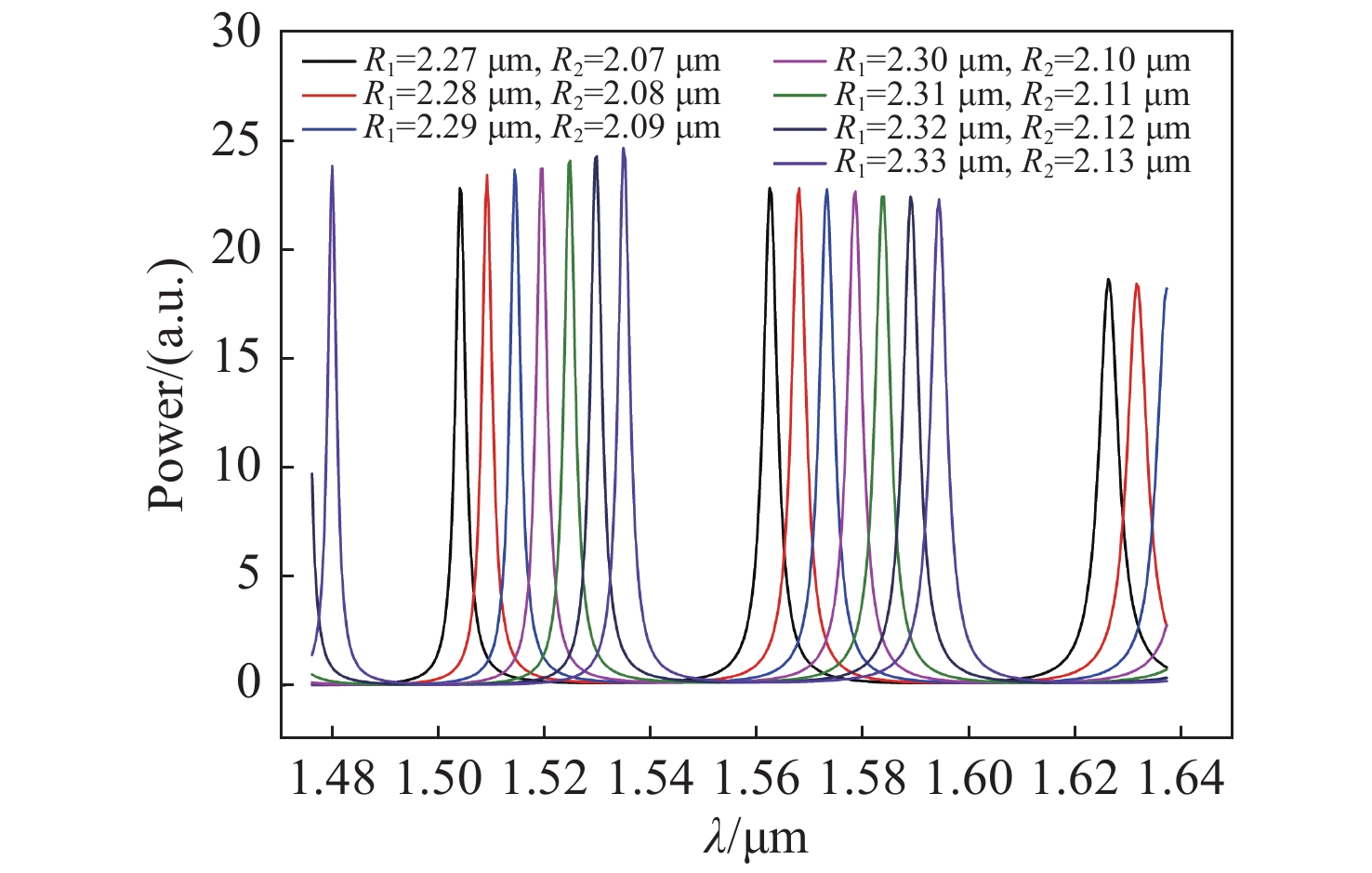
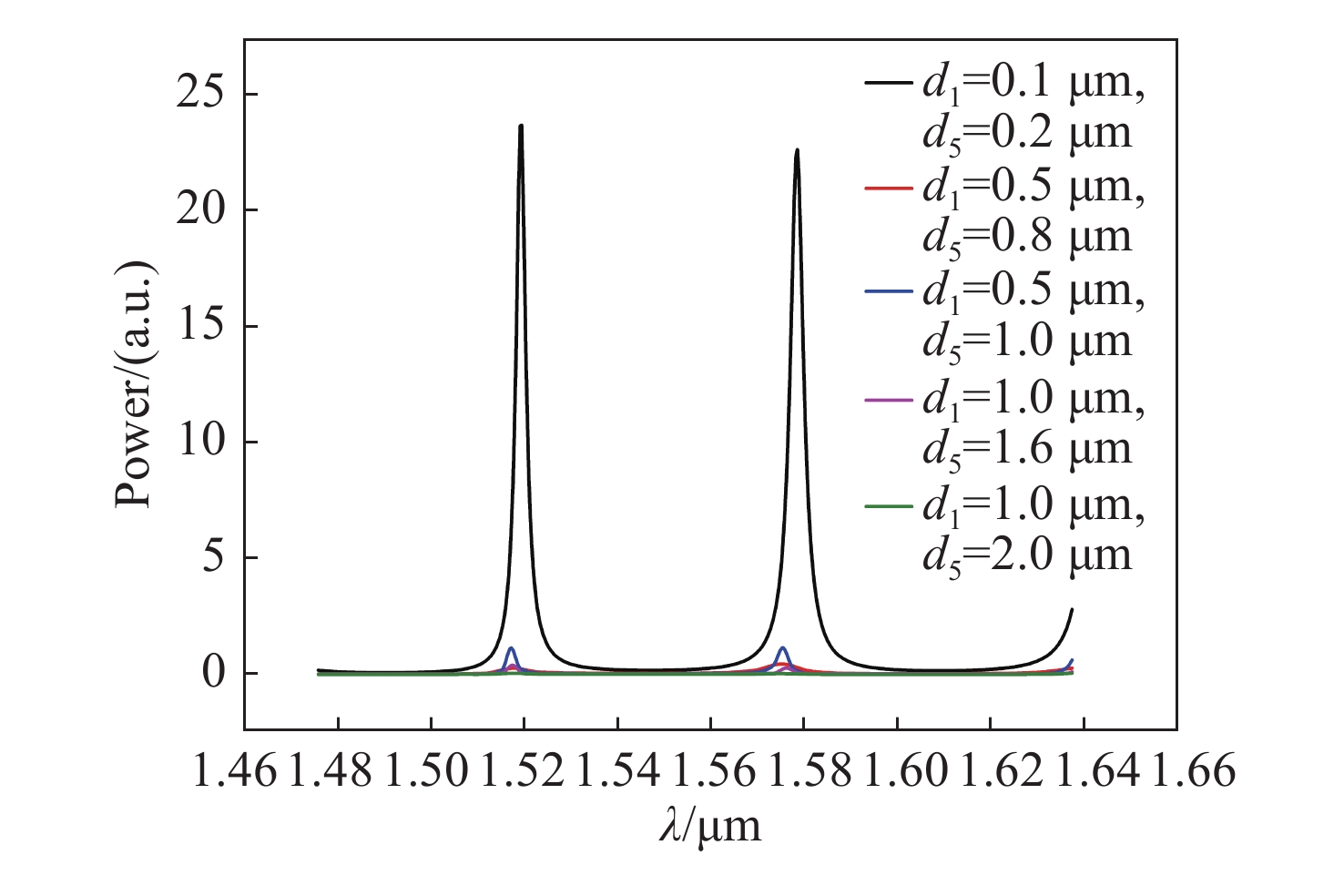
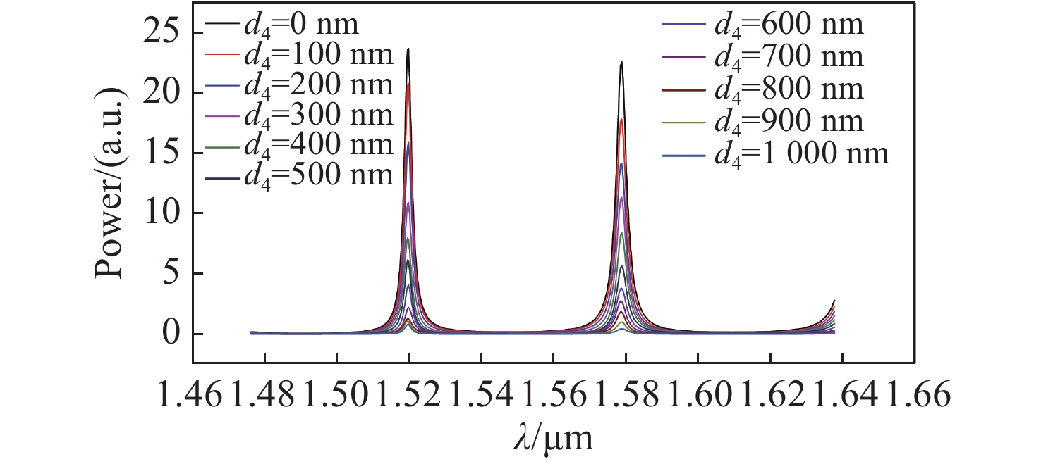
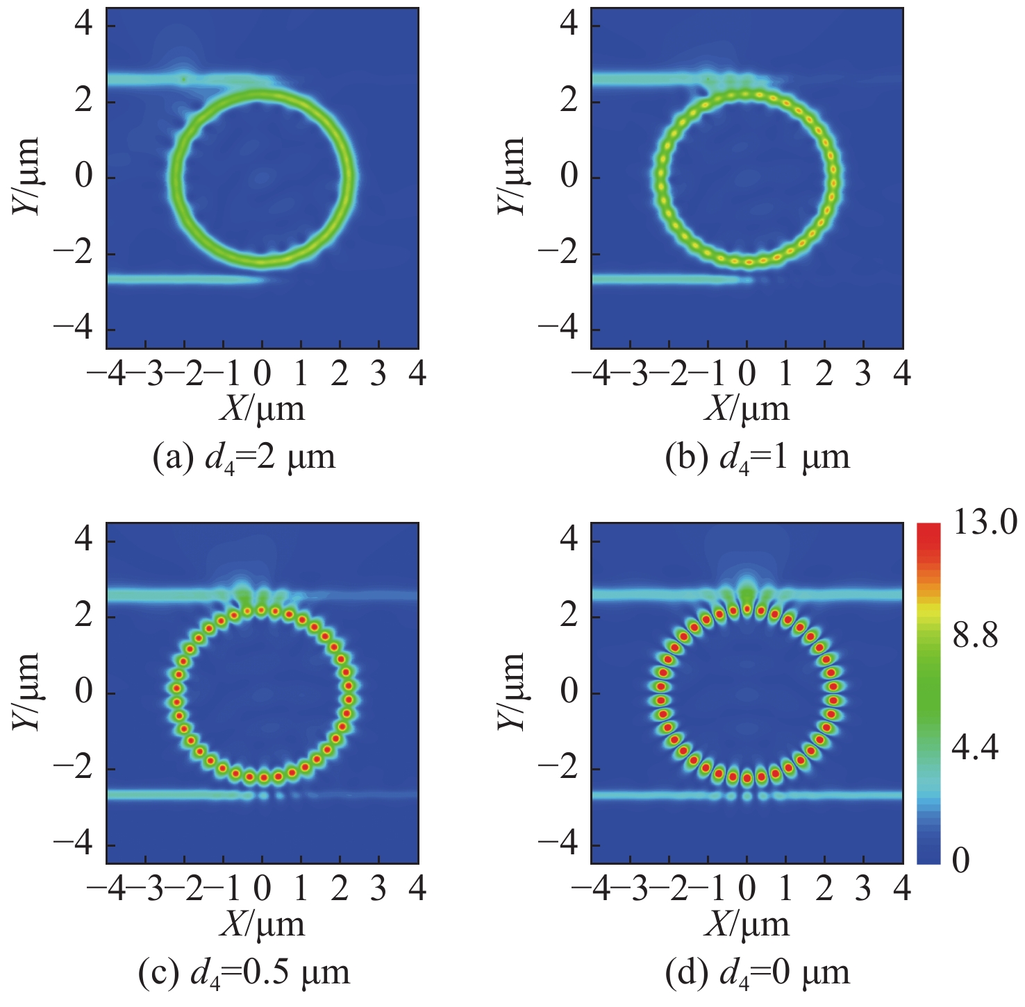
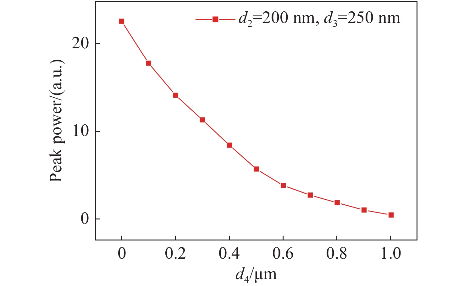
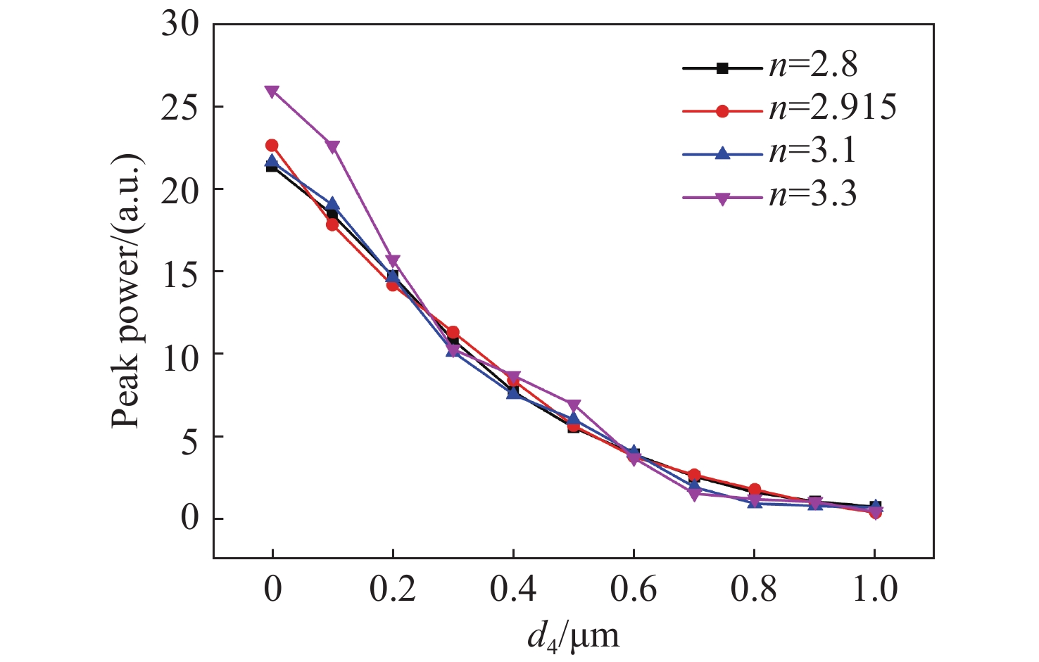
In order to measure the micro-displacement of a fluorescent substance, we propose a nanofluidic channel-resonant cavity structure. Firstly, by using the Finite-Difference Time-Domain (FDTD) method, the influences of the quantum dot’s polarization state and structural parameters on the coupling effect of fluorescence and structure are studied and the structure is optimized. Then, the micro-displacement of the fluorescent substance is detected by measuring the change in the optical power output of the coupled structure. Finally, the factors affecting the sensitivity of the sensors are studied. The results show that, compared with the traditional method, when the refractive index of the nanofluidic channel-resonant cavity coupling structure is in the 2.8~3.3 range, the structure can sense of the micro-displacement of a fluorescent substance with high accuracy. The results also show that the sensing sensitivity can be further improved by reducing the distance between the nanofluidic channel and the resonant cavity.
In order to measure the micro-displacement of a fluorescent substance, we propose a nanofluidic channel-resonant cavity structure. Firstly, by using the Finite-Difference Time-Domain (FDTD) method, the influences of the quantum dot’s polarization state and structural parameters on the coupling effect of fluorescence and structure are studied and the structure is optimized. Then, the micro-displacement of the fluorescent substance is detected by measuring the change in the optical power output of the coupled structure. Finally, the factors affecting the sensitivity of the sensors are studied. The results show that, compared with the traditional method, when the refractive index of the nanofluidic channel-resonant cavity coupling structure is in the 2.8~3.3 range, the structure can sense of the micro-displacement of a fluorescent substance with high accuracy. The results also show that the sensing sensitivity can be further improved by reducing the distance between the nanofluidic channel and the resonant cavity.


2021, 14(1): 153-162.
doi: 10.37188/CO.2020-0148
cstr: 32171.14.CO.2020-0148
Abstract:
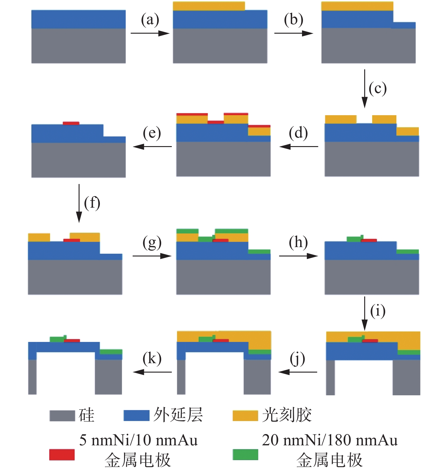
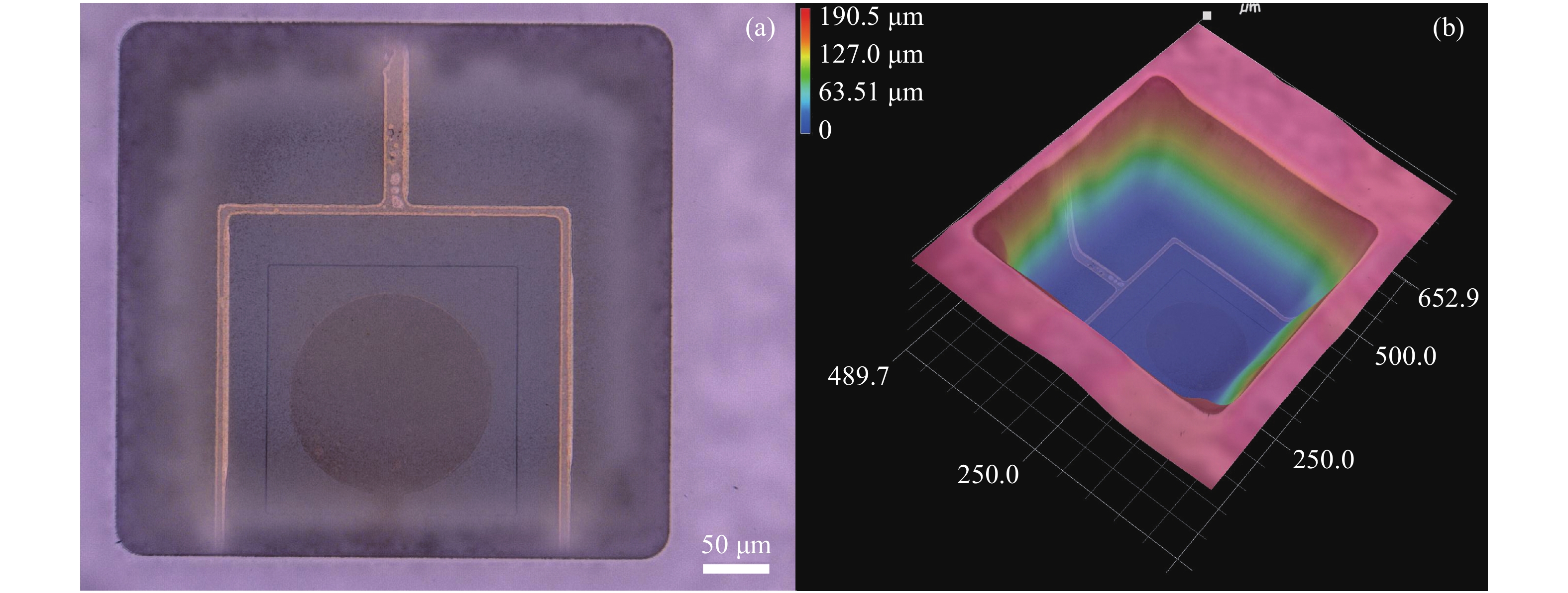
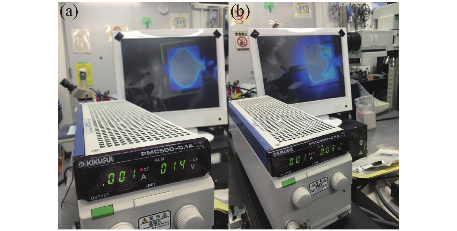
In order to improve the opto-electronic performance and light extraction efficiency of LEDs based on a GaN-on-silicon platform, we proposed an LED device based on GaN-on-silicon with an ultra-thin freestanding membrane. By combining photolithography, deep reactive ion etching and inductively-coupled plasma reactive ion etching, we prepared an LED based on a GaN-on-silicon platform with an ultra-thin freestanding membrane, removing the silicon substrate of light-emitting area and most area of the electrodes, and thinning most of the GaN epitaxial layer. We performed three-dimensional morphology characterization for the LED device and found that the surface of the LED’s membrane is flat and that the membrane’s deformation is minimal. It is proved that the back process can solve the problem of membrane deformation caused by stress release between the GaN epitaxial layer and the silicon substrate. By characterizing the current-voltage and electroluminescence spectrum of the LED and comparing the LEDs with different structures and different light-emitting area sizes, we found that the opto-electronic performance and light output efficiency of the LED with an ultra-thin freestanding membrane are better than that of the common LED, and the change in size of the light-emitting area has a significant effect on the performance of the LED. Compared with the current of common LED, the current of the LED which has an ultra-thin freestanding membrane with 80-μm diameter light-emitting area increased from 4.3 mA to 23.9 mA under 15 V driving voltage. Under 3-mA current, the peak light intensity increased by about 5 times. The light-emitting efficiency of the LED with a 120-μm diameter light-emitting area is improved more perceptibly compared with that of LED with a 80-μm diameter light-emitting area. This research provides more possibilities for the development of high-performance LED devices with an ultra-thin freestanding membrane.
In order to improve the opto-electronic performance and light extraction efficiency of LEDs based on a GaN-on-silicon platform, we proposed an LED device based on GaN-on-silicon with an ultra-thin freestanding membrane. By combining photolithography, deep reactive ion etching and inductively-coupled plasma reactive ion etching, we prepared an LED based on a GaN-on-silicon platform with an ultra-thin freestanding membrane, removing the silicon substrate of light-emitting area and most area of the electrodes, and thinning most of the GaN epitaxial layer. We performed three-dimensional morphology characterization for the LED device and found that the surface of the LED’s membrane is flat and that the membrane’s deformation is minimal. It is proved that the back process can solve the problem of membrane deformation caused by stress release between the GaN epitaxial layer and the silicon substrate. By characterizing the current-voltage and electroluminescence spectrum of the LED and comparing the LEDs with different structures and different light-emitting area sizes, we found that the opto-electronic performance and light output efficiency of the LED with an ultra-thin freestanding membrane are better than that of the common LED, and the change in size of the light-emitting area has a significant effect on the performance of the LED. Compared with the current of common LED, the current of the LED which has an ultra-thin freestanding membrane with 80-μm diameter light-emitting area increased from 4.3 mA to 23.9 mA under 15 V driving voltage. Under 3-mA current, the peak light intensity increased by about 5 times. The light-emitting efficiency of the LED with a 120-μm diameter light-emitting area is improved more perceptibly compared with that of LED with a 80-μm diameter light-emitting area. This research provides more possibilities for the development of high-performance LED devices with an ultra-thin freestanding membrane.


2021, 14(1): 163-169.
doi: 10.37188/CO.2020-0198
cstr: 32171.14.CO.2020-0198
Abstract:
In order to reduce the size of spectrometers and make it suitable for military satellites and other fields, we used colloidal quantum dots as filter materials to study the optical properties of CdSe colloidal quantum dot filters. The high-quality CdSe colloidal quantum dots were synthesized by an organic phase reaction method and prepared into CdSe colloidal quantum dots thin film filters after p-phenylenediamine extinction treatment. The Transmission Electron Microscope (TEM) was used to characterize the morphology and particle size of the as-prepared samples. The UV-visible absorption and UV-visible transmittance were measured at different temperatures. The results indicated that the increase in particle size caused both absorption and transmittance to increase for CdSe colloidal quantum dots thin film filters at room temperature. Under a given particle size, the absorption and transmittance of the first exciton absorption peak red shifted with the rise in temperature. The red shift of absorption curve of CdSe colloidal quantum dots thin film filters did not exceed 1nm per 10 K temperature rising and the half-width increased. In addition, the stability and tunable characteristics of the CdSe colloidal quantum dots thin film filters have been verified through repeated experiments, and it is suitable as a cut-off filter. Therefore, CdSe colloidal quantum dots thin film filters have high value in micro-spectrometers.
In order to reduce the size of spectrometers and make it suitable for military satellites and other fields, we used colloidal quantum dots as filter materials to study the optical properties of CdSe colloidal quantum dot filters. The high-quality CdSe colloidal quantum dots were synthesized by an organic phase reaction method and prepared into CdSe colloidal quantum dots thin film filters after p-phenylenediamine extinction treatment. The Transmission Electron Microscope (TEM) was used to characterize the morphology and particle size of the as-prepared samples. The UV-visible absorption and UV-visible transmittance were measured at different temperatures. The results indicated that the increase in particle size caused both absorption and transmittance to increase for CdSe colloidal quantum dots thin film filters at room temperature. Under a given particle size, the absorption and transmittance of the first exciton absorption peak red shifted with the rise in temperature. The red shift of absorption curve of CdSe colloidal quantum dots thin film filters did not exceed 1nm per 10 K temperature rising and the half-width increased. In addition, the stability and tunable characteristics of the CdSe colloidal quantum dots thin film filters have been verified through repeated experiments, and it is suitable as a cut-off filter. Therefore, CdSe colloidal quantum dots thin film filters have high value in micro-spectrometers.


2021, 14(1): 170-181.
doi: 10.37188/CO.2020-0145
cstr: 32171.14.CO.2020-0145
Abstract:
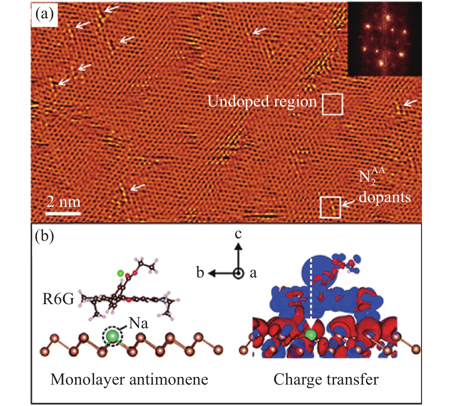
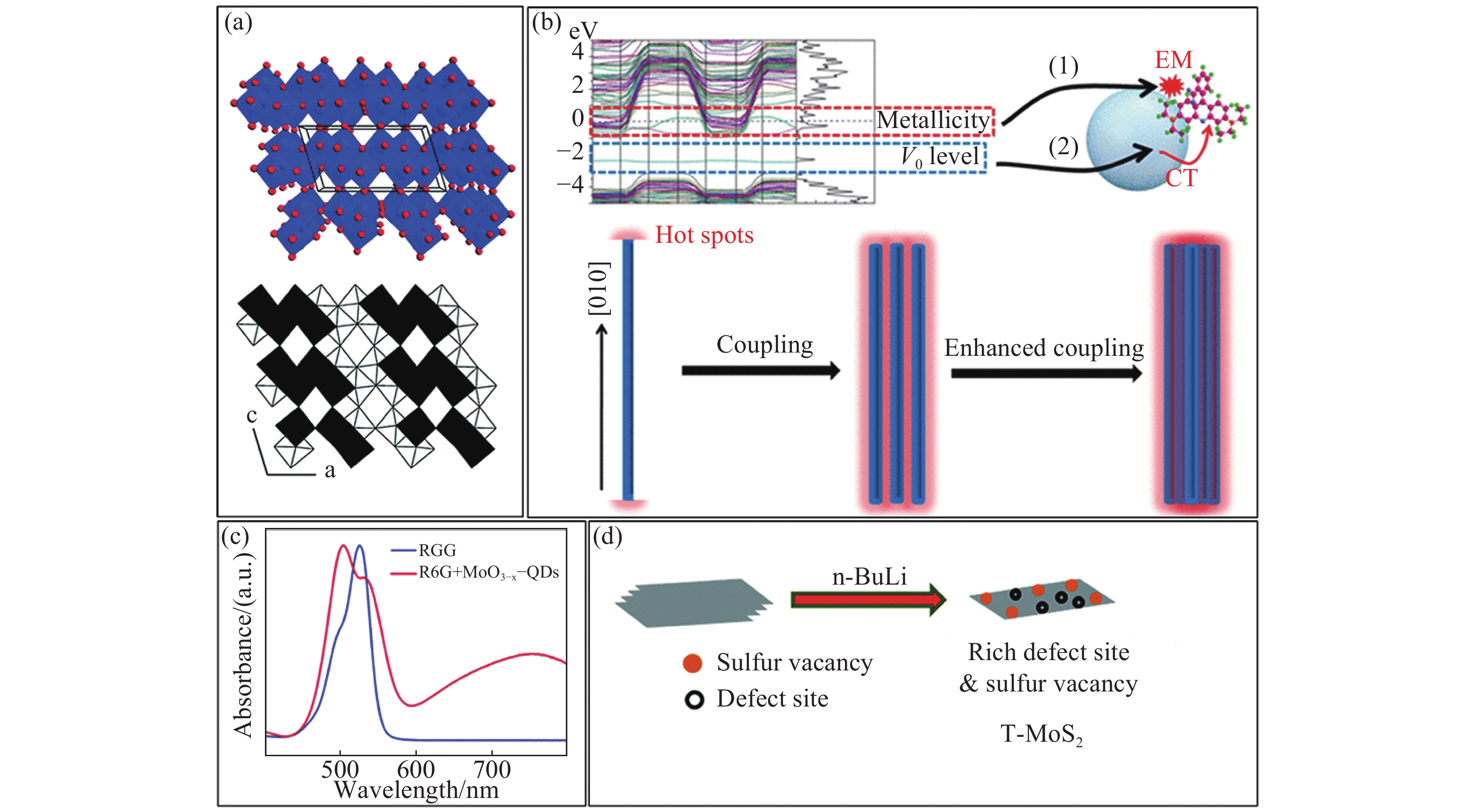
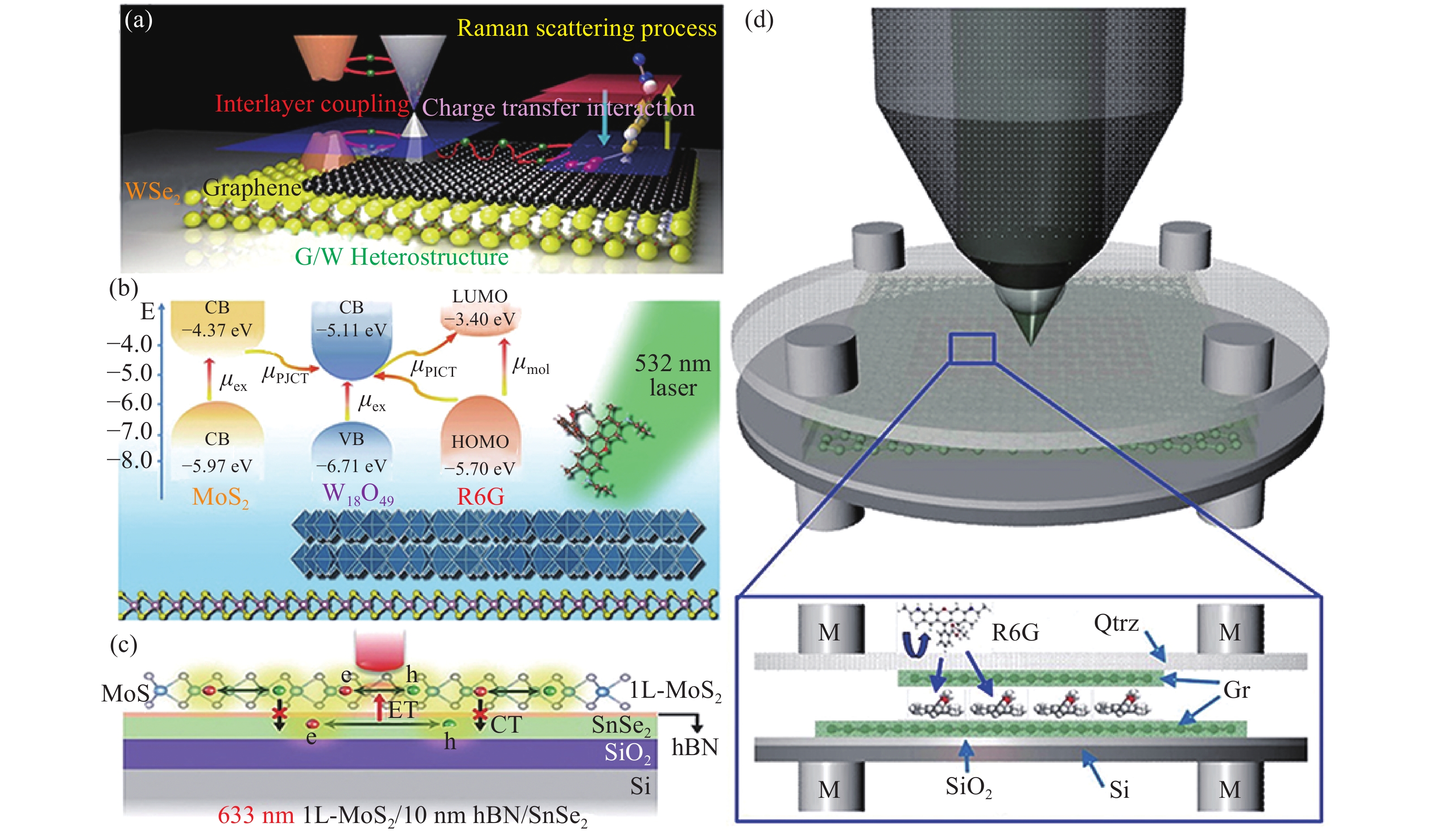
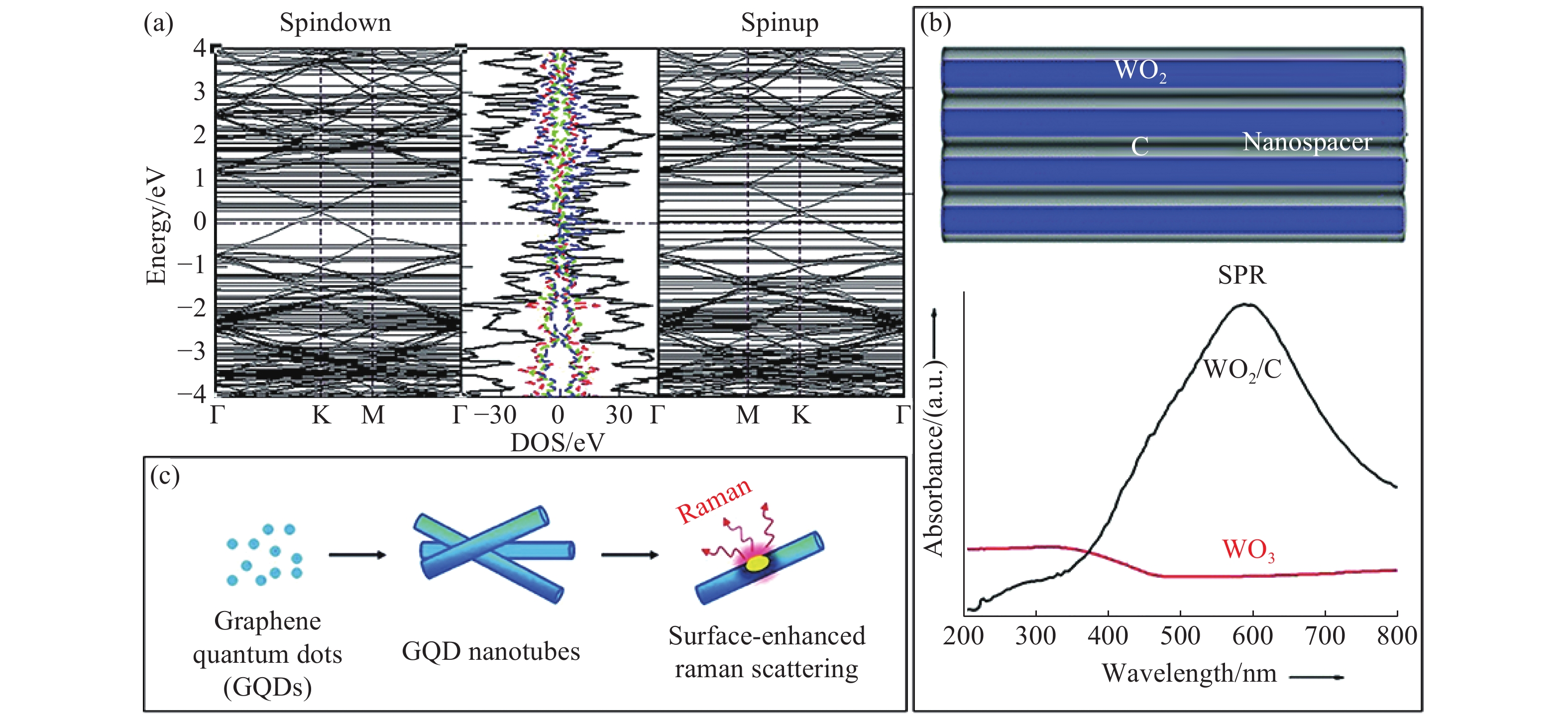
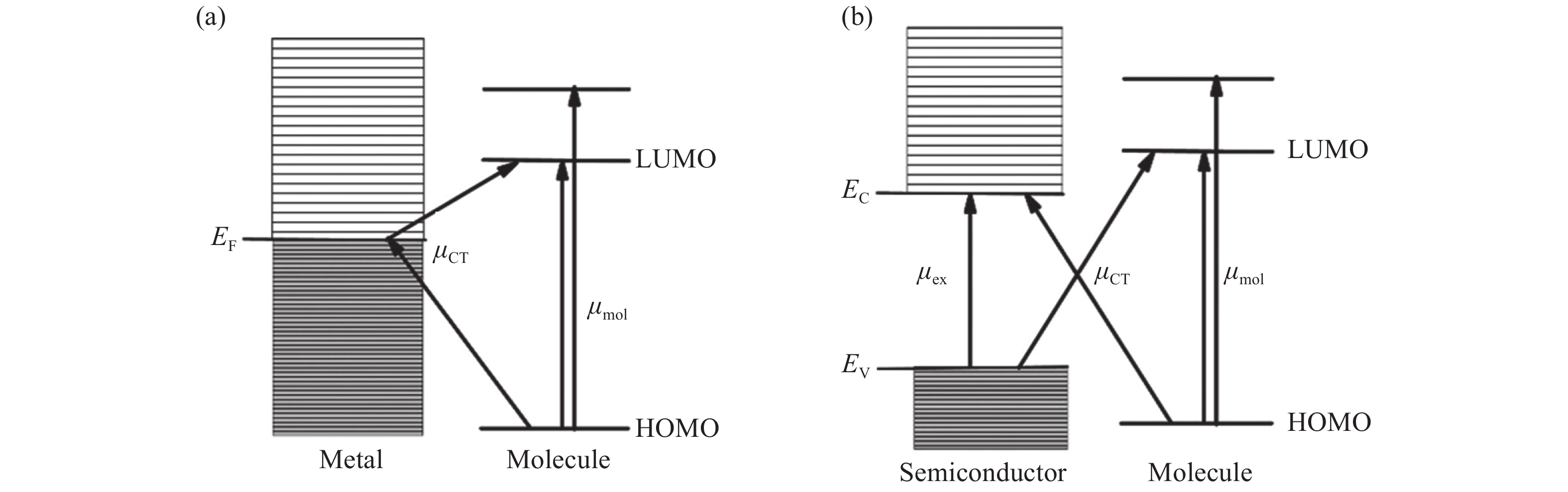
In recent years, a series of new low-dimensional optoelectronic materials with excellent properties have emerged. Combined with surface-enhanced Raman scattering (SERS) technology, they show great application potential and are expected to become highly sensitive SERS substrates. Defects and interface regulation of low-dimensional optoelectronic materials are important strategies for their applications in SERS technology. In this paper, the types and enhancement mechanisms of defects- and interface-enhanced Raman scattering in new low-dimensional optoelectronic materials are introduced. By looking forward to the application and research prospect of defects- and interface-enhanced Raman scattering, this work might inspire people to reconsider and further understand the study of SERS.
In recent years, a series of new low-dimensional optoelectronic materials with excellent properties have emerged. Combined with surface-enhanced Raman scattering (SERS) technology, they show great application potential and are expected to become highly sensitive SERS substrates. Defects and interface regulation of low-dimensional optoelectronic materials are important strategies for their applications in SERS technology. In this paper, the types and enhancement mechanisms of defects- and interface-enhanced Raman scattering in new low-dimensional optoelectronic materials are introduced. By looking forward to the application and research prospect of defects- and interface-enhanced Raman scattering, this work might inspire people to reconsider and further understand the study of SERS.


2021, 14(1): 182-195.
doi: 10.37188/CO.2020-0175
cstr: 32171.14.CO.2020-0175
Abstract:
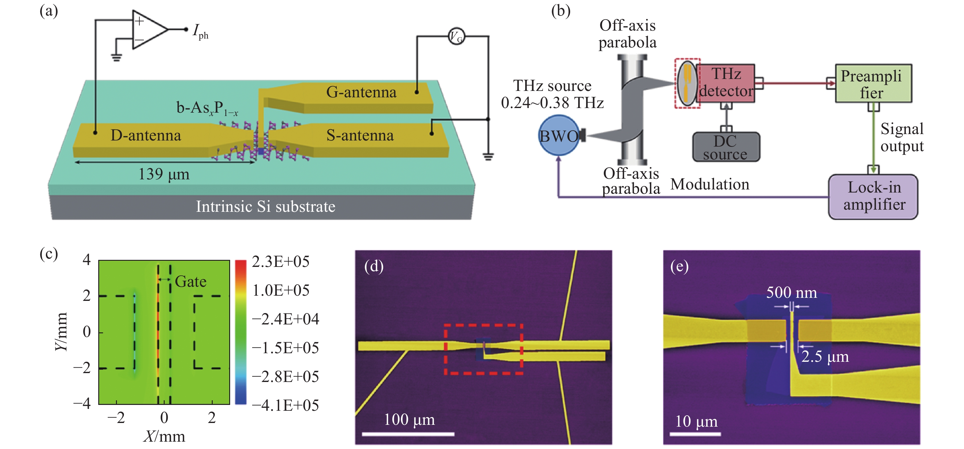
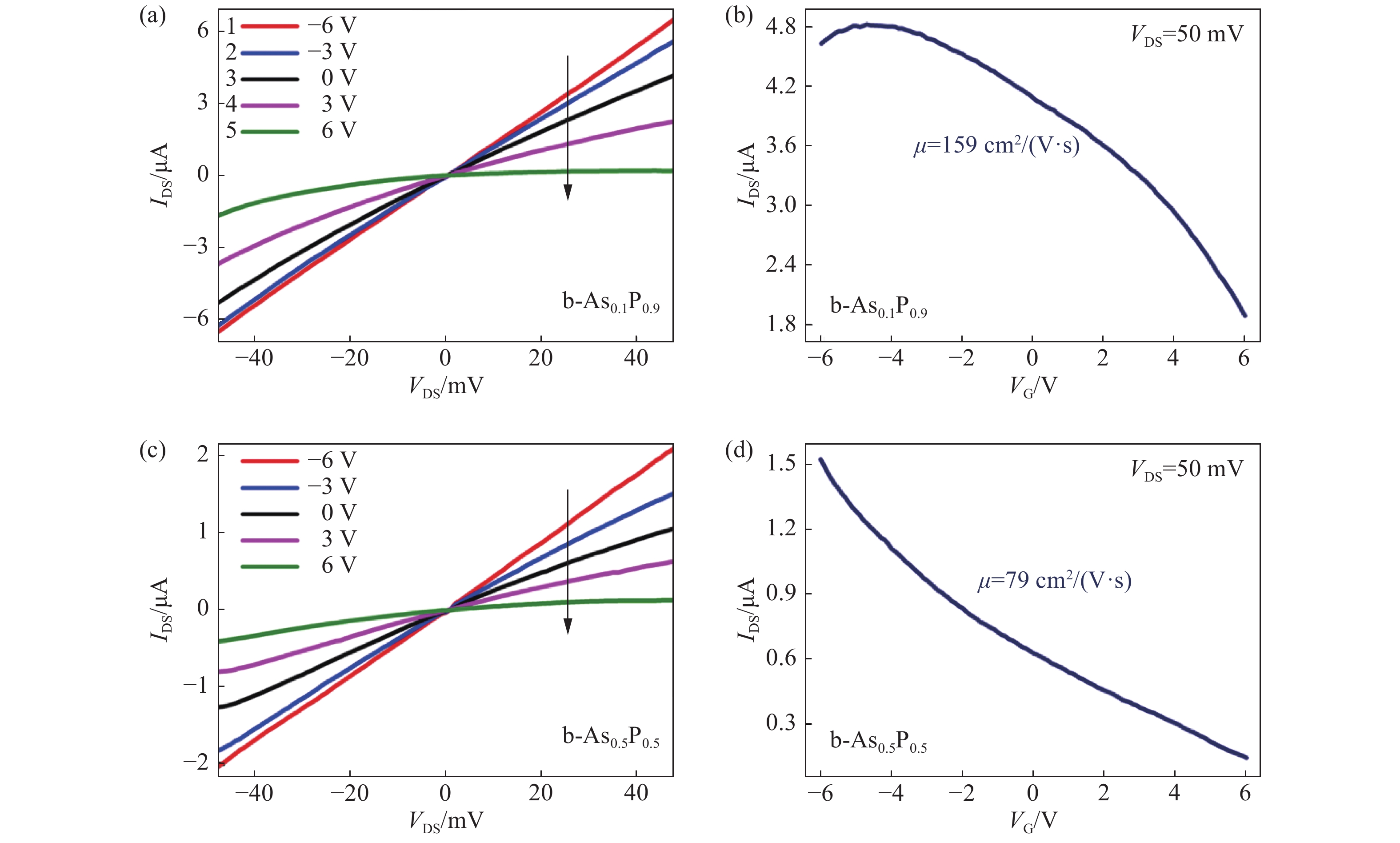
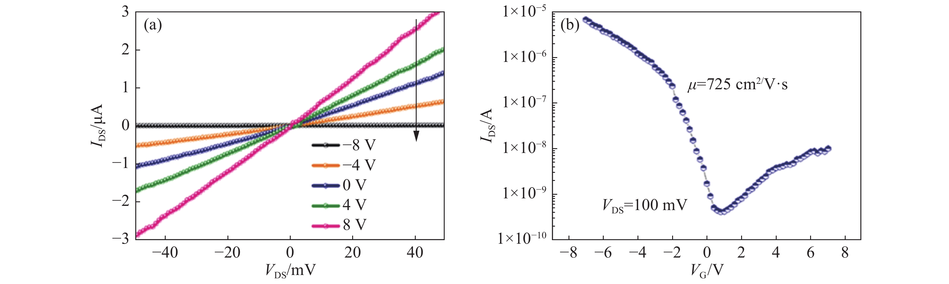
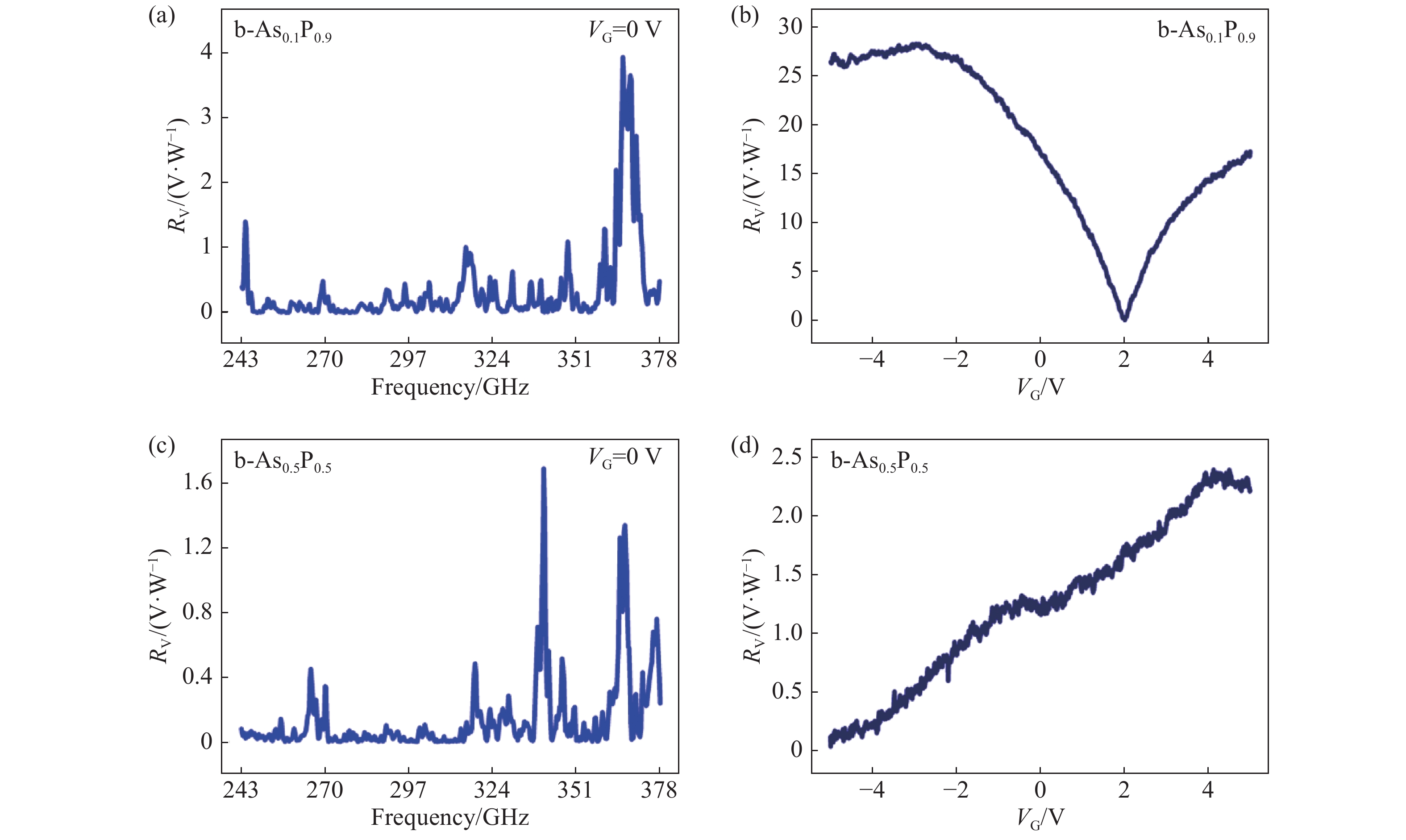
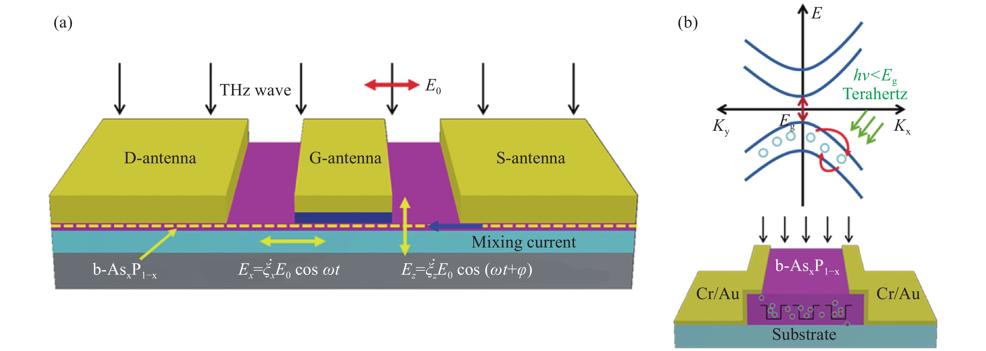
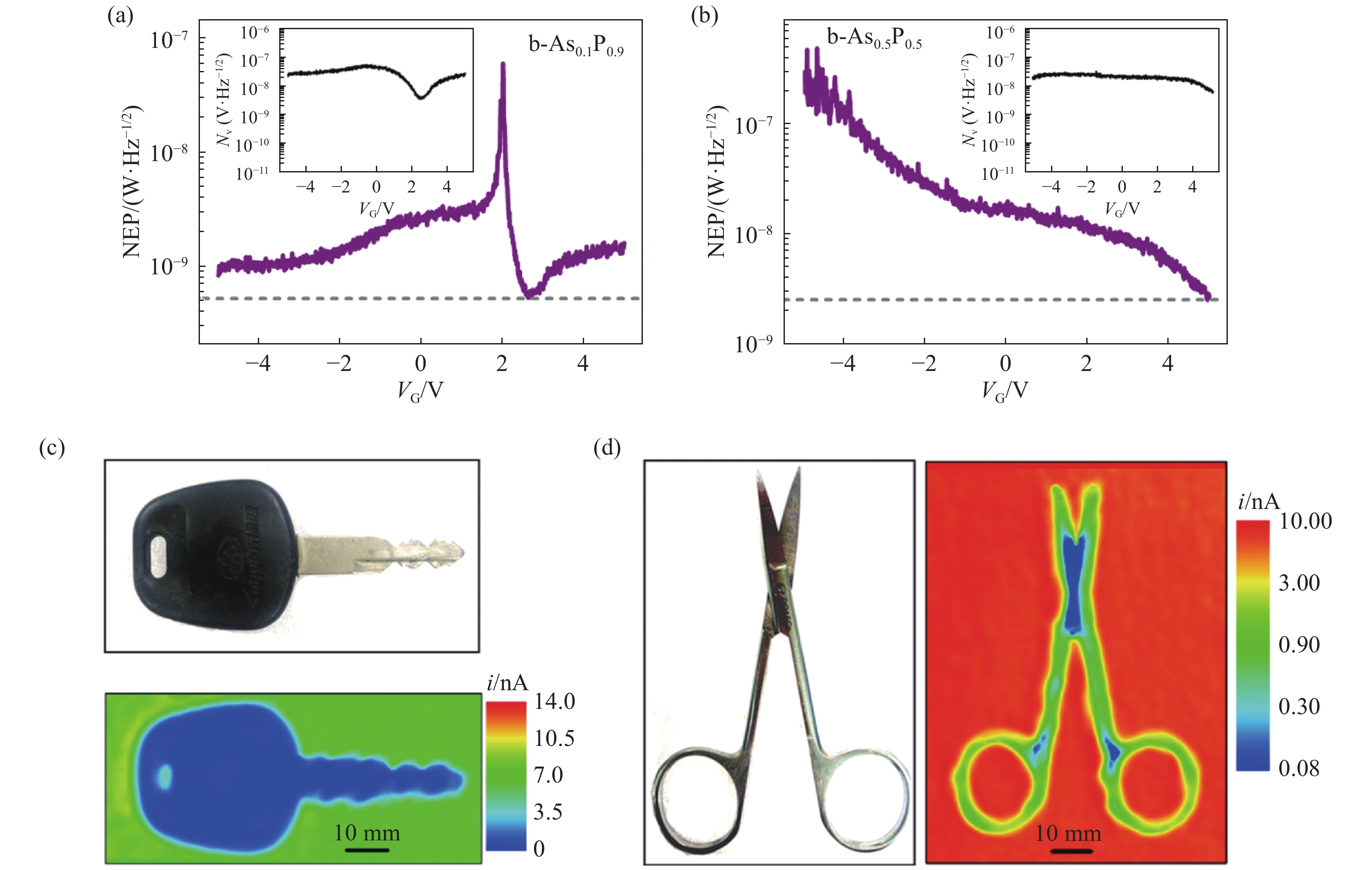
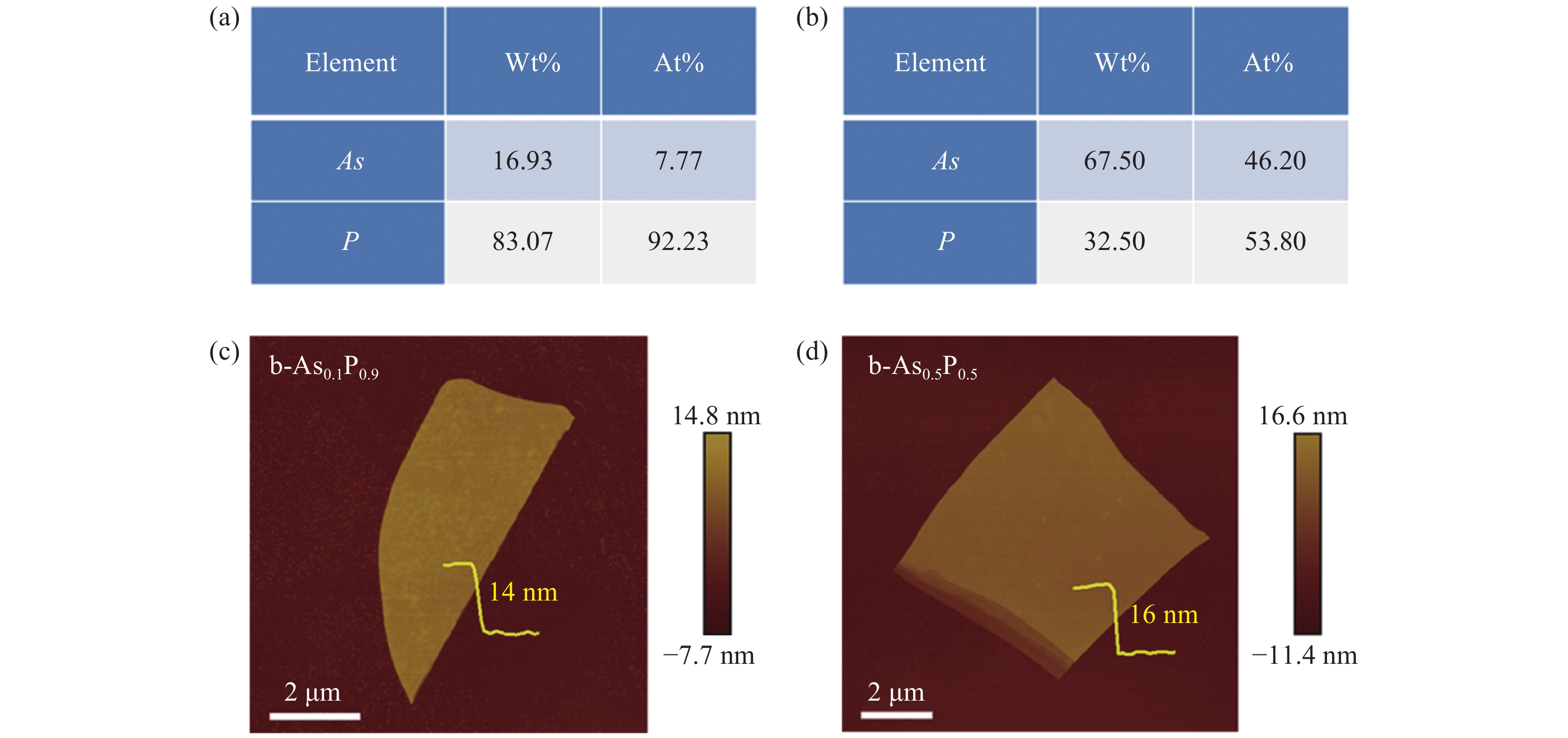
Terahertz technology is indispensable in plenty of fields due to the abundant interactions between terahertz waves and matter. In order to meet the needs of terahertz applications, the development of highly sensitive and portable terahertz detectors based on distinctive physical mechanisms and various materials with excellent properties are urgently required. Black arsenic-phosphorus is a novel two-dimensional material that has a tunable band gap and transport characteristics with varying chemical composition, which has gained widespread interest in optoelectronic applications. Recent research on b-AsxP1-x mainly focuses on infrared detection, while the detection of terahertz has not yet been applied. Herein, an antenna-coupled terahertz detector based on exfoliated multilayer black arsenic-phosphorus is demonstrated. The terahertz response performance of the detector reflects two different mechanisms, which have a competitive relationship in the detection process. In particular, the detection mechanism can be tailored by varying the chemical composition of black arsenic-phosphorus. By balancing the band gap and carrier mobility, a responsivity of over 28.23 V/W and a noise equivalent power of less than 0.53 nW/Hz1/2 are obtained at 0.37 THz. This implies that black arsenic-phosphorus has great potential in terahertz technology.
Terahertz technology is indispensable in plenty of fields due to the abundant interactions between terahertz waves and matter. In order to meet the needs of terahertz applications, the development of highly sensitive and portable terahertz detectors based on distinctive physical mechanisms and various materials with excellent properties are urgently required. Black arsenic-phosphorus is a novel two-dimensional material that has a tunable band gap and transport characteristics with varying chemical composition, which has gained widespread interest in optoelectronic applications. Recent research on b-AsxP1-x mainly focuses on infrared detection, while the detection of terahertz has not yet been applied. Herein, an antenna-coupled terahertz detector based on exfoliated multilayer black arsenic-phosphorus is demonstrated. The terahertz response performance of the detector reflects two different mechanisms, which have a competitive relationship in the detection process. In particular, the detection mechanism can be tailored by varying the chemical composition of black arsenic-phosphorus. By balancing the band gap and carrier mobility, a responsivity of over 28.23 V/W and a noise equivalent power of less than 0.53 nW/Hz1/2 are obtained at 0.37 THz. This implies that black arsenic-phosphorus has great potential in terahertz technology.


2021, 14(1): 196-205.
doi: 10.37188/CO.2020-0062
cstr: 32171.14.CO.2020-0062
Abstract:
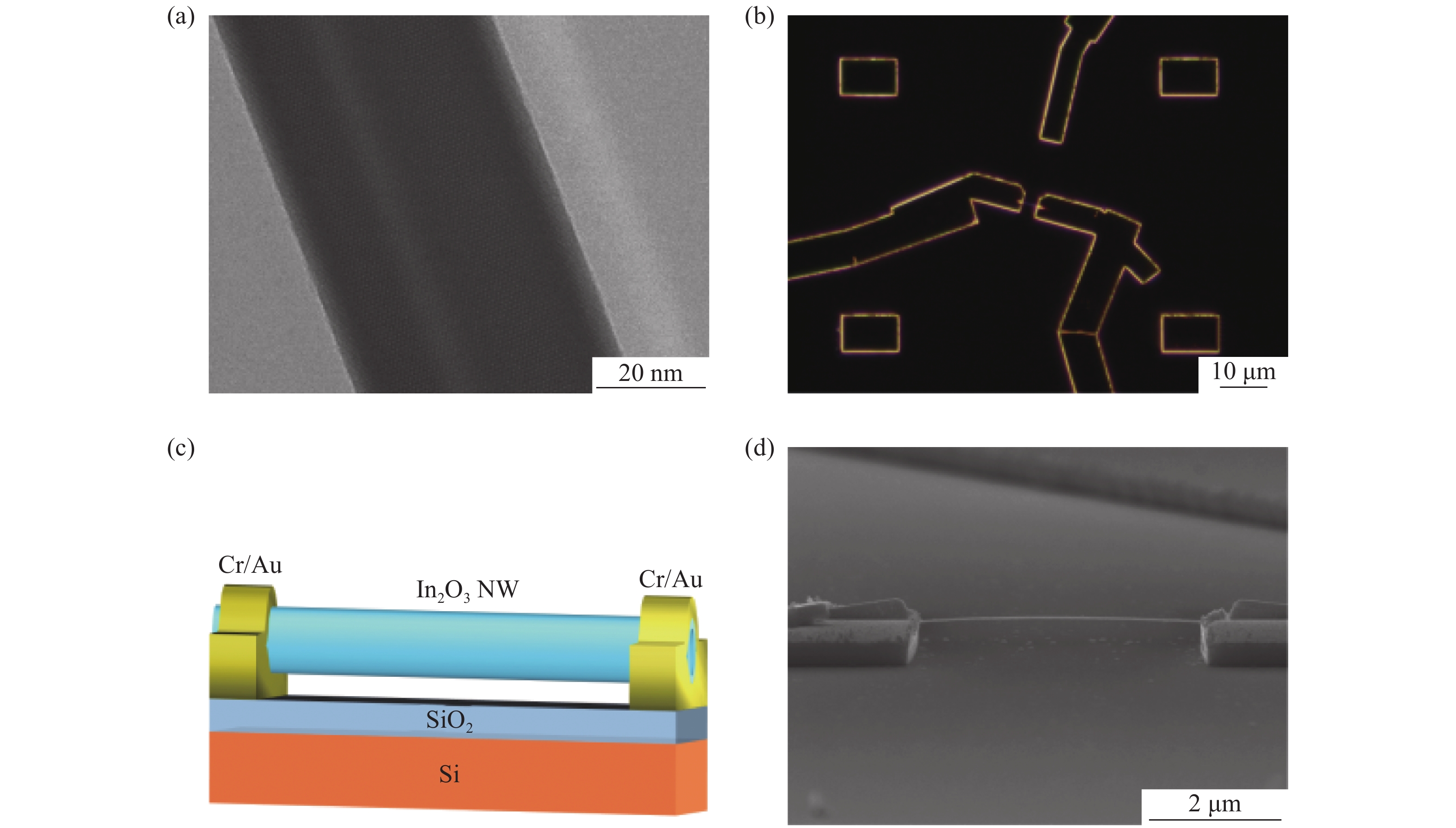
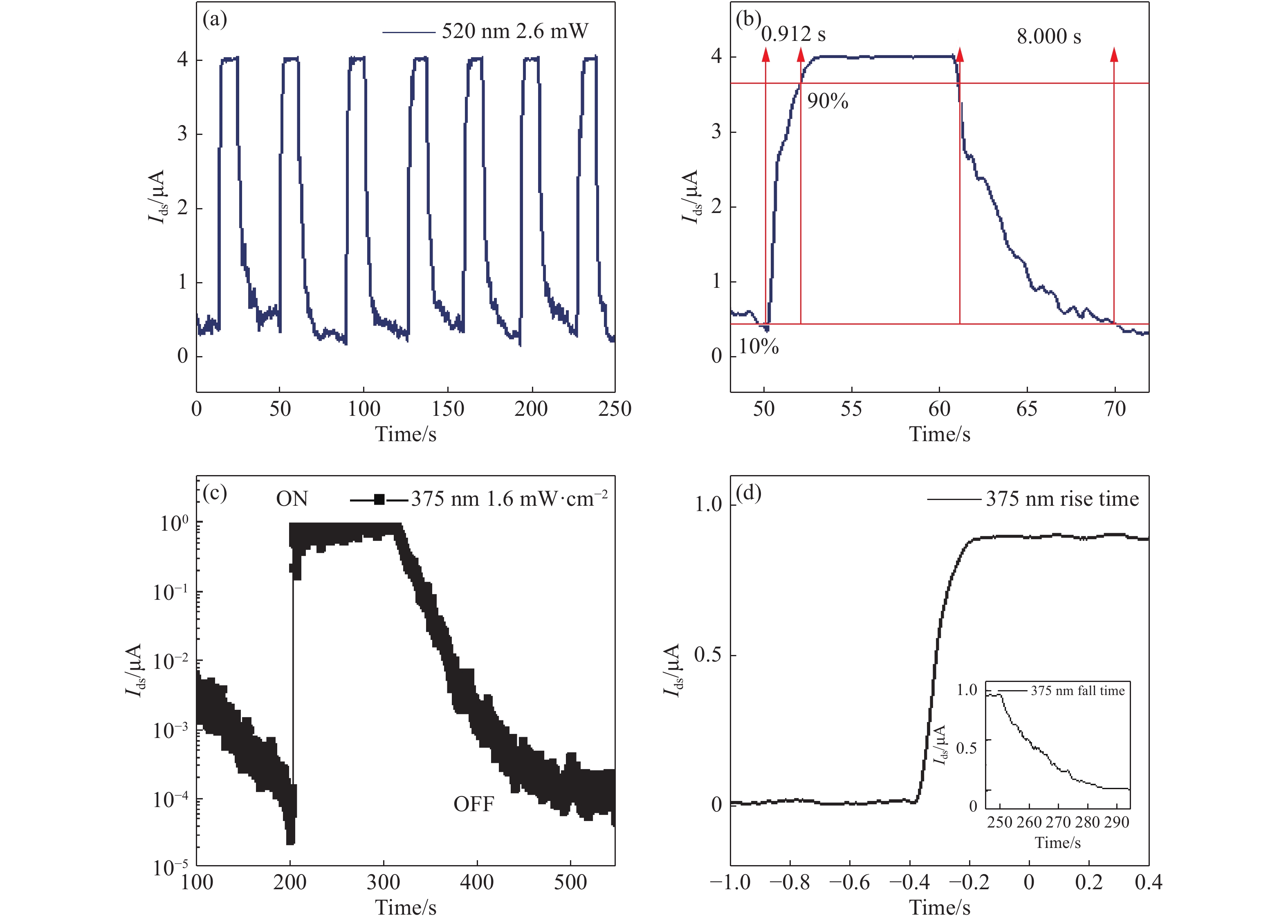
One-dimensional (1D) semiconductor nanowires have shown outstanding performance in nano-electronics and nano-photonics. However, the electrical properties of the nanowire transistors are very sensitive to interactions between the nanowires and substrates. Optimizing the device structure can improve the electrical and photodetection performance of nanowire transistors. We report a suspended In2O3 nanowire transistor fabricated by one-step lithography, showing a high mobility of 54.6 cm2V−1s−1 and a low subthreshold swing of 241.5 mVdec−1. As an ultraviolet photodetector, the phototransistor shows an extremely low dark current (~10−13 A) and a high responsivity of 1.6×10⁵ A•W−1. This simple and effective method of suspending the channel material of a transistor can be widely used in manufacturing high-performance micro-nano devices.
One-dimensional (1D) semiconductor nanowires have shown outstanding performance in nano-electronics and nano-photonics. However, the electrical properties of the nanowire transistors are very sensitive to interactions between the nanowires and substrates. Optimizing the device structure can improve the electrical and photodetection performance of nanowire transistors. We report a suspended In2O3 nanowire transistor fabricated by one-step lithography, showing a high mobility of 54.6 cm2V−1s−1 and a low subthreshold swing of 241.5 mVdec−1. As an ultraviolet photodetector, the phototransistor shows an extremely low dark current (~10−13 A) and a high responsivity of 1.6×10⁵ A•W−1. This simple and effective method of suspending the channel material of a transistor can be widely used in manufacturing high-performance micro-nano devices.


2021, 14(1): 206-212.
doi: 10.37188/CO.2020-0153
cstr: 32171.14.CO.2020-0153
Abstract:
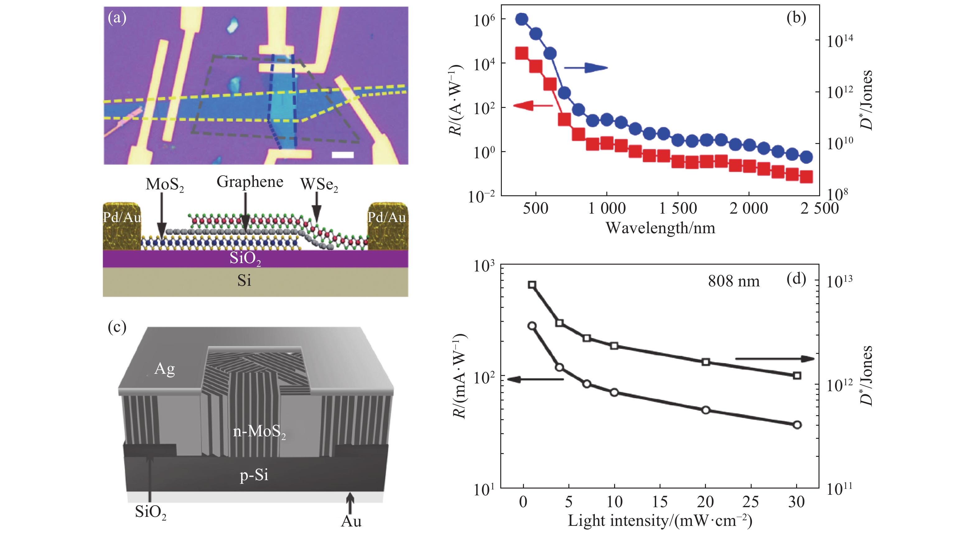
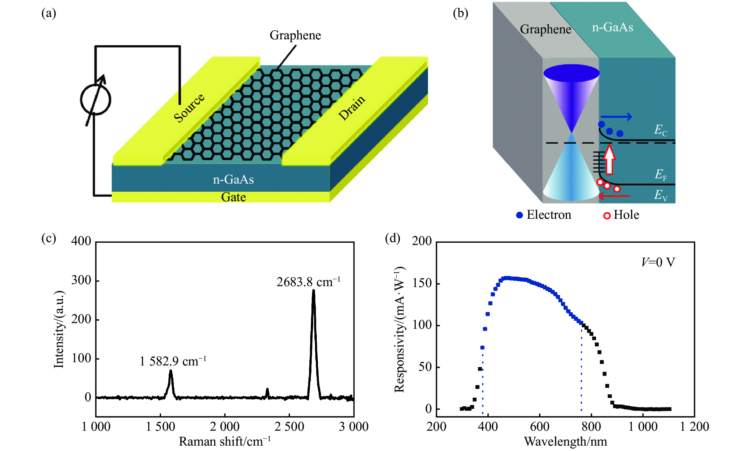
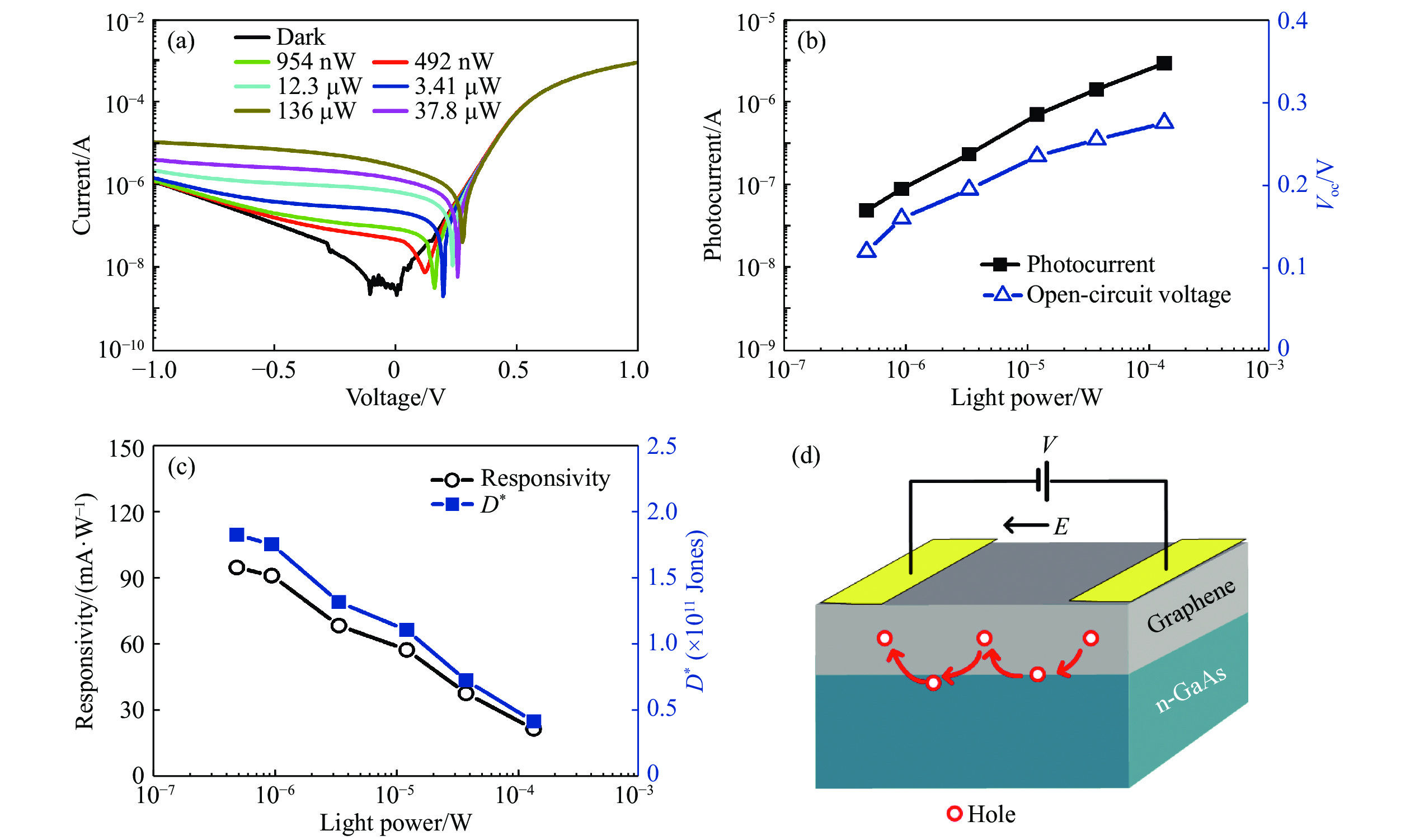
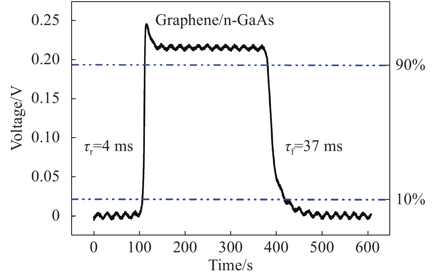
Hybrid graphene/semiconductor phototransistors have attracted great attention because of their ultrahigh responsivity. However, the specific detectivity (D*) for such hybrid phototransistors obtained from source-drain electrodes is assumed to be 1/f noise. In this paper, D* of ~1.82×10¹¹ Jones was achieved from source-gate electrodes. Compared with the same device which was measured from source-drain electrodes, D* was improved by ~500 times. This could be attributed to the carrier trapping and detrapping processes having been screened by the Schottky barrier at the interface. The rise and decay times were 4 ms and 37 ms, respectively. The temporal response speed also correspondingly improved by ~2 orders of magnitude. This work provides an alternative route toward light photodetectors with high specific detectivity and speed.
Hybrid graphene/semiconductor phototransistors have attracted great attention because of their ultrahigh responsivity. However, the specific detectivity (D*) for such hybrid phototransistors obtained from source-drain electrodes is assumed to be 1/f noise. In this paper, D* of ~1.82×10¹¹ Jones was achieved from source-gate electrodes. Compared with the same device which was measured from source-drain electrodes, D* was improved by ~500 times. This could be attributed to the carrier trapping and detrapping processes having been screened by the Schottky barrier at the interface. The rise and decay times were 4 ms and 37 ms, respectively. The temporal response speed also correspondingly improved by ~2 orders of magnitude. This work provides an alternative route toward light photodetectors with high specific detectivity and speed.

2021, 14(1): 213-225.
doi: 10.37188/CO.2020-0101
cstr: 32171.14.CO.2020-0101
Abstract:
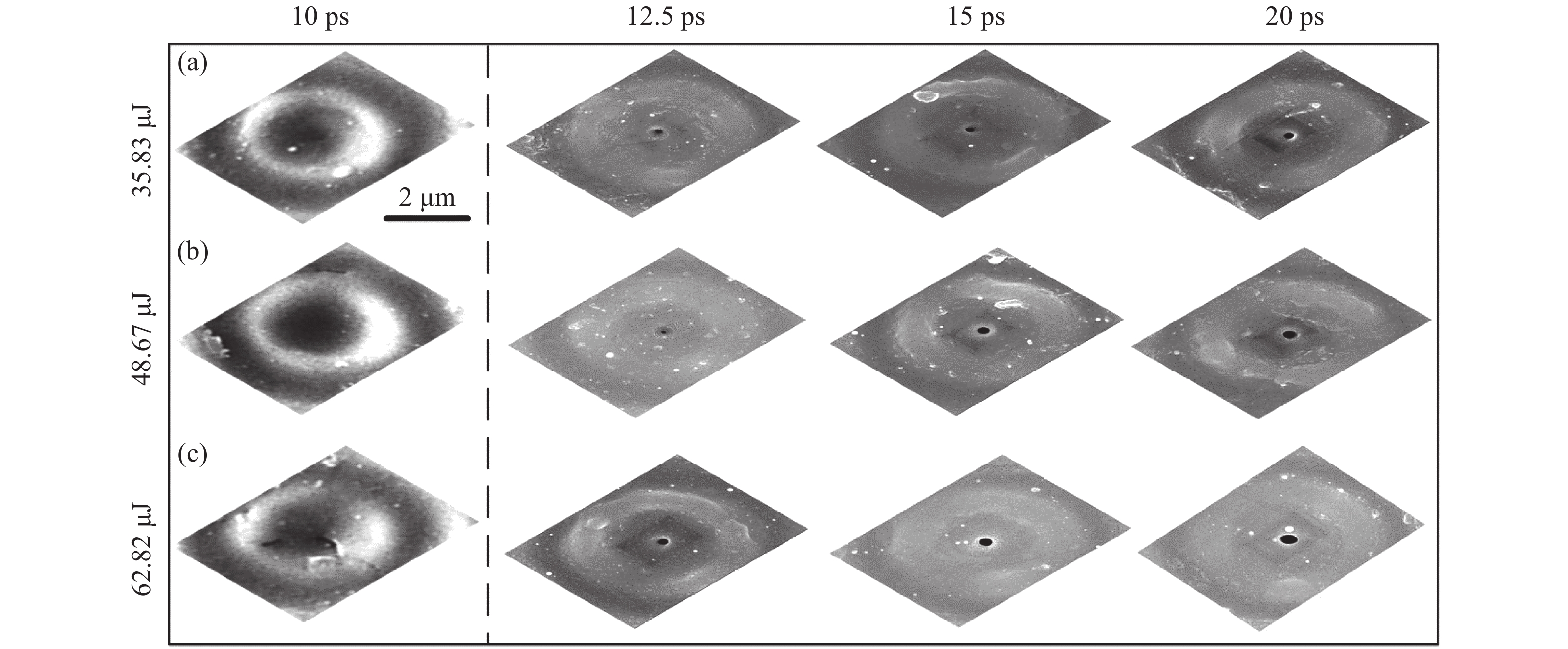
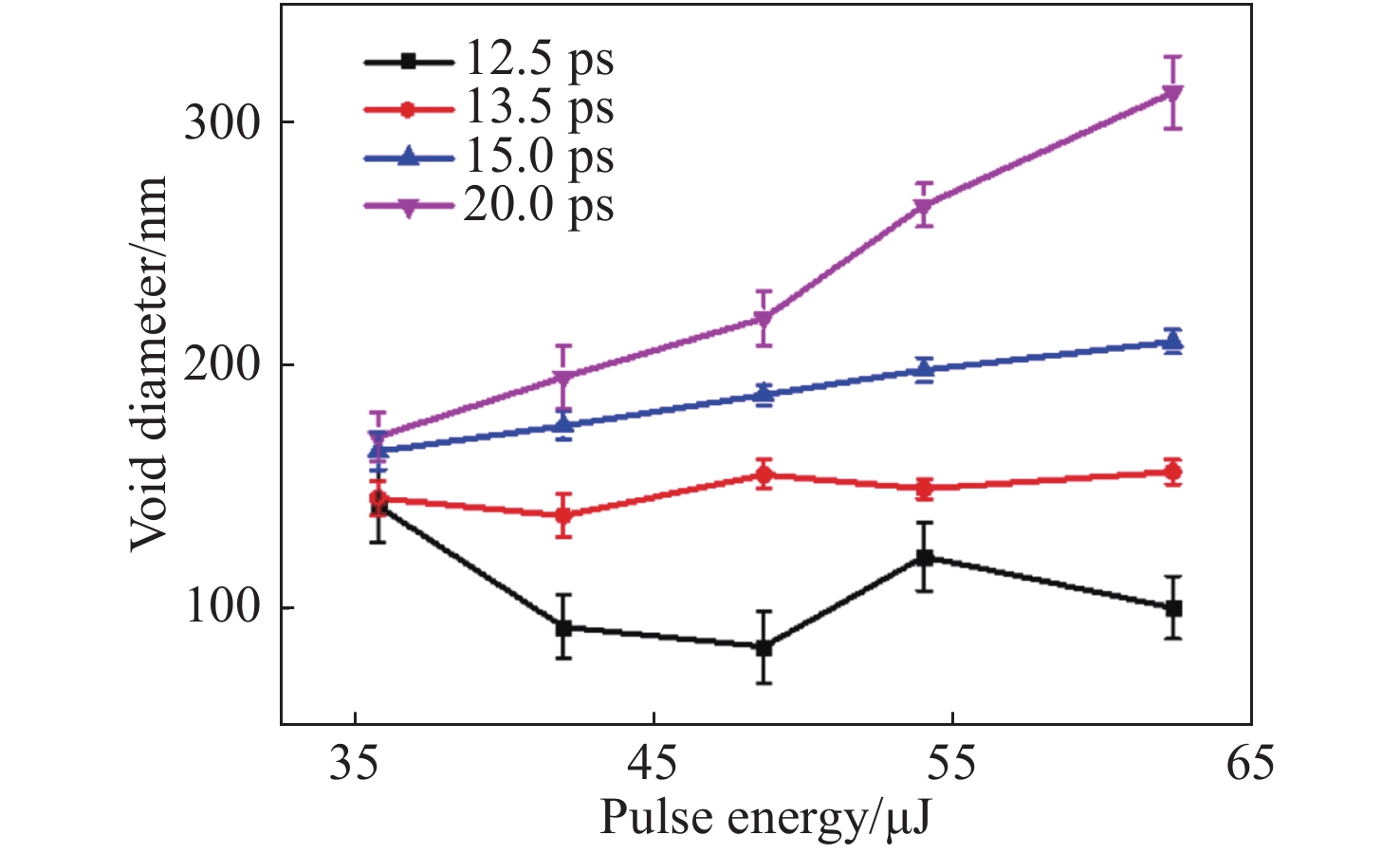
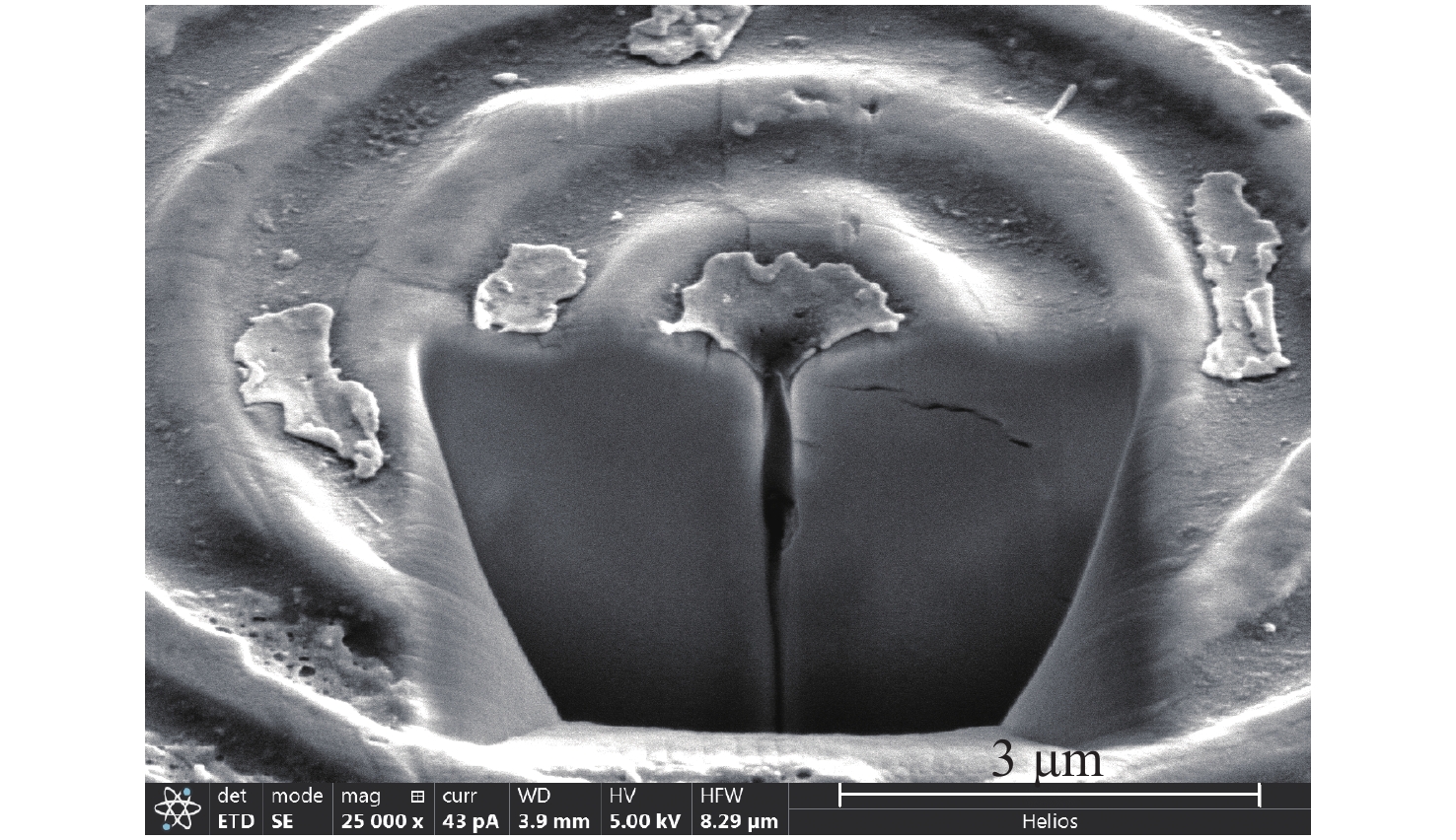
Zinc sulfide (ZnS) crystal is one of the important materials used to make the wide-spectrum infrared window. The ultrafast laser technology for manufacturing the nanopores with high aspect ratio provides an important approach to fabricate the photonic devices such as mid-infrared waveguide Fourier transform spectrometer etc. In this paper, a 40-times-demagnification ultrafast laser direct-writing system was built with a 4f system and a Gaussian-Bessel beam generated by a quartz axicon and a Yb:KGW laser source that operated at a wavelength of 1030 nm, a repetition rate of 100 kHz and a pulse width tunable from 223 fs to 20 ps. When the pulse energy was changed from 36 μJ to 63 μJ and the pulse duration was changed from 12.5 ps to 20 ps, the nanopore structure with a diameter of 80~320 nm was successfully written on the ZnS crystal. The surface morphology, diameter and depth of the nanopores were determined by FIB (Focused Ion Beams) ablation and SEM (Scanning Electron Microscopy) imaging. The influence of laser pulse energy and pulse width on the nanopores was studied. The results show that when the pulse width is 20 ps and the pulse energy is 48 µJ, the depth of a nanopore is about 270 µm.
Zinc sulfide (ZnS) crystal is one of the important materials used to make the wide-spectrum infrared window. The ultrafast laser technology for manufacturing the nanopores with high aspect ratio provides an important approach to fabricate the photonic devices such as mid-infrared waveguide Fourier transform spectrometer etc. In this paper, a 40-times-demagnification ultrafast laser direct-writing system was built with a 4f system and a Gaussian-Bessel beam generated by a quartz axicon and a Yb:KGW laser source that operated at a wavelength of 1030 nm, a repetition rate of 100 kHz and a pulse width tunable from 223 fs to 20 ps. When the pulse energy was changed from 36 μJ to 63 μJ and the pulse duration was changed from 12.5 ps to 20 ps, the nanopore structure with a diameter of 80~320 nm was successfully written on the ZnS crystal. The surface morphology, diameter and depth of the nanopores were determined by FIB (Focused Ion Beams) ablation and SEM (Scanning Electron Microscopy) imaging. The influence of laser pulse energy and pulse width on the nanopores was studied. The results show that when the pulse width is 20 ps and the pulse energy is 48 µJ, the depth of a nanopore is about 270 µm.