Latest Articles

 Abstract
 FullText HTML
 PDF 4328KB
Owing to the limited interfacial contact area, insufficient carrier transport efficiency, and the adverse effects of intrinsic defects in ZnO on photoresponse, further improvement in the performance of conventional ZnO/GaN heterojunction ultraviolet photodetectors remains restricted. To address these issues, Ga+Al co-doped ZnO nanorod arrays with different Ga doping concentrations were grown on porous p-GaN/Al2O3 substrates by a low-temperature hydrothermal method, and the corresponding Ga+Al co-doped ZnO nanorod/porous GaN heterojunctions were fabricated. The porous p-GaN structure was used to enhance heterojunction interfacial contact and light absorption, while Ga+Al co-doping was employed to regulate the defect states and carrier transport properties of ZnO nanorods, thereby improving the self-powered ultraviolet photodetection performance of the devices. The findings of the study demonstrated that under 365 nm ultraviolet illumination at 0 V bias, the device with a Ga doping concentration of 3 at.% exhibited the best UV photodetection performance, with a light/dark current ratio of


The circular swallowtail beams have recently exhibited better autofocusing ability and more tunability compared with low-order Airy or Pearcey catastrophe beams. However our attention is paid to exploring their metasurface generation and dynamics propagation of directional circular swallowtail (DCS) beams carrying power-exponent-phase vortices based on all-dielectric metasurfaces using finite-difference time-domain (FDTD) method, where the directional phase related to launch angles in


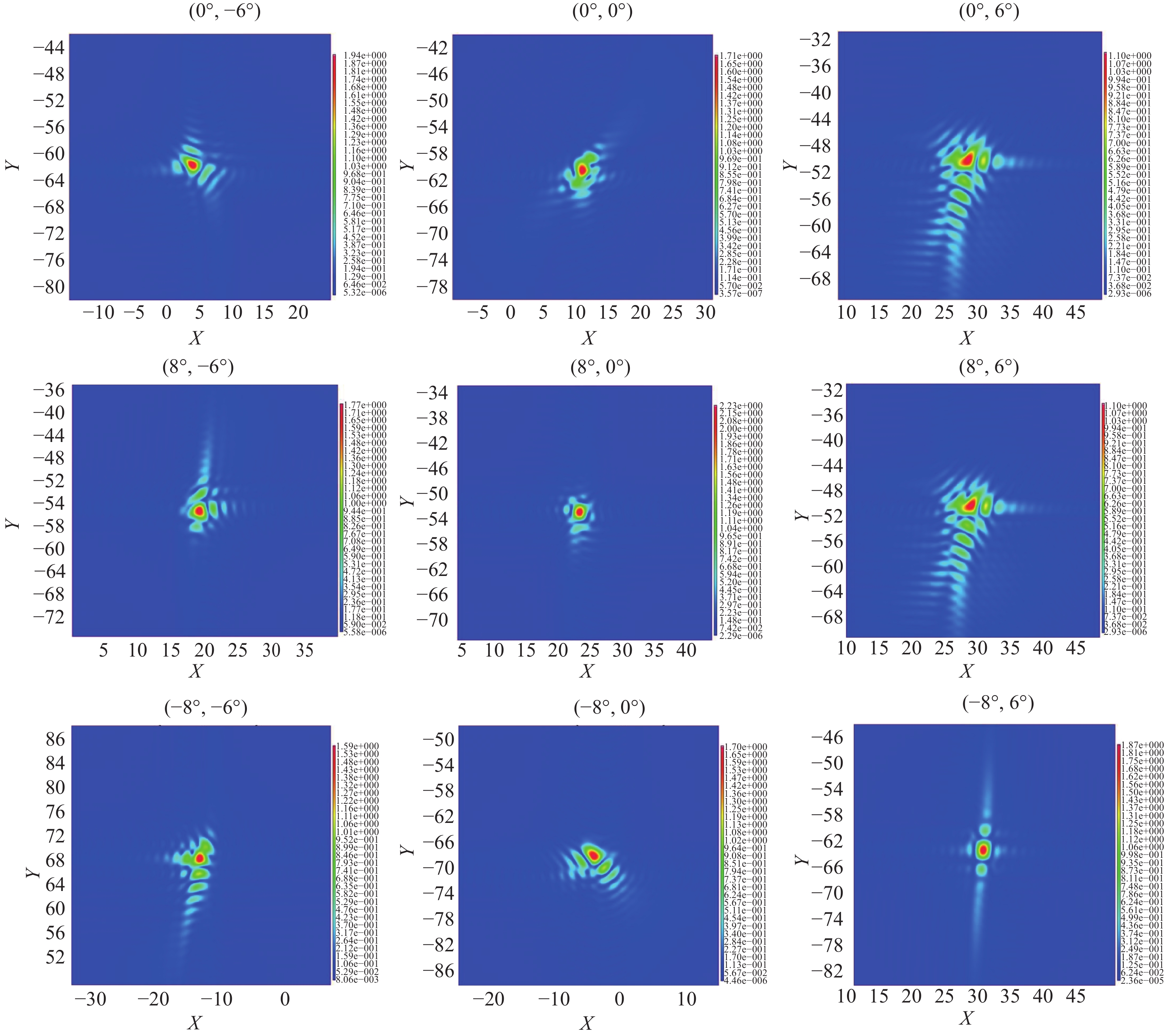
The quality of underwater imaging significantly deteriorates due to underwater light field which caused by multiple scattering of water. In order to quantitatively analyze the quality degradation of underwater image, it is necessary to study the distribution of underwater light field and establish a strict underwater image transmission model. Assuming that water volumn scattering function (VSF) is spherical symmetry, underwater light field distribution formed by an ideal point light source is calculated, and then water point spread function (PSF) is obtained by brightness integral along the path. Finally, water modulation transfer function (MTF) in the spherical space is derived by means of mathematical tools such as spherical harmonic function and spherical convolution. Under the condition that the intrinsic optical parameters of water are known, curves of water MTF and contrast limit factor are presented. The algorithm model solves the derivation of water MTF under the condition of spherical water VSF, laying a foundation for the derivation of water MTF under the condition of non-spherical water VSF and dynamic light field.


In response to the significant challenges posed by the width and uniformity of illumination from visual sensors during the inspection of sharp corner welds, high-speed welding, and the welding of highly reflective materials in the laser welding process, the influence of line laser width on inspection accuracy was analyzed in this paper. To meet the requirements of narrow width and high uniformity, a line laser shaping design based on a Diffractive Optical Element (DOE) and a Powell prism was proposed. The light generated by a semiconductor laser with a wavelength of 405 nm was shaped into an ideal Gaussian beam using a DOE after beam expansion and collimation, and subsequently shaped into a line laser using a Powell prism. A model was constructed to simulate the aforementioned process, and corresponding experiments were designed to verify the relationship between line laser width and inspection accuracy. The results showed that after passing through the DOE, the


To address the issues of high noise and low accuracy in solar meridian extraction using a single polarization mode, we propose a dual-polarization mode fusion method. First, the method preprocesses the polarization field using the interquartile range method. Then, by combining the mirror symmetry of the degree of linear polarization with the anti-symmetry of the polarization angle and applying complex domain transformation along with radial-azimuthal segmentation analysis, the method fuses global and local polarization features. Finally, temporal filtering is applied based on solar motion law and the neutral point constraint, further improving extraction accuracy. Experimental evaluations under diverse conditions demonstrate that the complete pipeline achieves mean relative errors of 0.02 (sunny), 0.051 (cloudy), 0.053 (fog), and 0.017 (dust) against the astronomical solar azimuth references, substantially outperforming single-feature methods. This study not only provides a polarization-based heading reference for autonomous systems, but also offers a scalable computational paradigm for integrating global and local polarization features.


In order to achieve large-range dual-parameter tuning of laser output in repetition rate and pulse width for a Yb:YAG single-cavity thin-disk regenerative amplifier, we designed and constructed a dual Pockels cell collaboratively controlled single-cavity Yb:YAG thin-disk regenerative amplifier. Relying on the timing coordination of the dual Pockels cells and the design of a wide-stability-range resonator, it ensured high beam quality and high energy extraction efficiency, while flexibly achieving a wide range of adjustable laser repetition frequency output. Additionally, the adjustment of the output laser pulse width was achieved by changing the distance between the two compression gratings. Experimental results showed that the thin-disk regenerative amplifier achieved laser output with a tunable repetition frequency ranging from 1 to 50 kHz by regulating the Pockels cells. At a repetition frequency of 50 kHz and an average pump power of 503 W, a maximum output power of 93.1 W was obtained, with beam quality factors


Traditional intensity-based refractive index measurement methods are constrained by the classical diffraction limit and the shot noise limit, which severely restricts the improvement of measurement precision. To address this issue, a novel quantum measurement scheme integrating entangled coherent states (ECS) and parity detection (PD) is proposed. Taking advantage of the non-classical correlation of quantum entanglement, the scheme constructs a dual-mode entangled coherent state light source and realizes high-fidelity signal demodulation through a customized parity detection system. Theoretical derivation and numerical simulation results demonstrate that the measurement resolution of the proposed scheme breaks through the Rayleigh limit, achieving a


Addressing the requirement for infrared detection of ship wakes under complex sea conditions, a method for analyzing the dynamic infrared polarization characteristics of ship wakes based on the microfacet model is proposed. An analytical model for the infrared polarization effects of wakes against a complex sea surface background is constructed. Based on the P-M sea spectrum model and the Kelvin wake model, the microfacet bidirectional reflectance distribution function is introduced to analyze the infrared polarization characteristics of ship wakes under dynamic sea surface backgrounds. The influence of parameters such as ship speed, draught, wind speed, and wind direction on the wake's infrared polarization characteristics, including the degree of polarization (DOP), angle of polarization (AOP), and contrast, is investigated. Notably, the average contrast of the wake's infrared DOP image is improved by 159% compared to traditional intensity images, and the AOP image shows an improvement of 258%. The analytical model for wake infrared polarization effects is validated by comparing mathematical simulations with computational fluid dynamics simulations, achieving a similarity of over 95.7%. A comparison between actual captured wake images and simulation results shows high similarity, confirming the effectiveness of the proposed model for simulating and analyzing the infrared polarization characteristics of ship wakes against a sea background. This study provides an important theoretical foundation for high-precision, anti-interference detection and identification of ships under complex sea conditions.


A low-noise linear-polarization single longitudinal mode (SLM) fiber laser based on polarimetric parity-time (PT) symmetry is proposed and experimentally demonstrated. PT symmetry is achieved within a linear reflection structure. When the balanced gain–loss contrast surpasses the coupling coefficient, the condition for PT-symmetry breaking is met, enabling the realization of an SLM laser. Stable laser output with a high sidemode suppression ratio (SMSR) of 62.6 dB and a high optical signal-to-noise ratio (OSNR) of 64.32 dB is realized. The Lorentz linewidth is measured as 182.5 Hz. The degree of polarization (DOP) and polarization extinction ratio (PER) of the laser remain above 99.8 % and 30.8 dB within 4 hours. Furthermore, the relative intensity noise (RIN) and phase noise of the PT-symmetric laser are analyzed and compared with those of fiber lasers and semiconductor lasers. The results demonstrate the low-noise performance of the proposed PT-symmetric laser.


Supercontinuum (SC) generated from femtosecond laser filamentation has found extensive applications due to its broadband spectral properties. In this study, we present a novel method to simultaneously improve the spectral coverage and power density of SC. This is realized by combining two-color femtosecond laser injection and multi-filament array arrangement in fused silica. With this method, high spectral power SC is obtained. The spectral power density is above 0.1 mW/nm over a broad wavelength range from approximately 380 nm to 950 nm. We find that both the spectral range and power density of SC are affected by the input power and the intensity ratio between the fundamental and second-harmonic laser pulses. In addition, the spectral fluctuation of the generated SC is measured to be less than 4% within 6 minutes. These results offer a feasible and effective way to enhance the spectral power and coverage of SC sources. They are of great importance for promoting the practical applications of SC.


High-power, high-beam-quality short-pulse/ultrashort-pulse green lasers have wide applications in industry, medicine, and scientific research. To clarify the research progress of green light sources based on second-harmonic generation (SHG, frequency doubling), this paper systematically reviews the latest advancements in SHG green light sources at kilohertz repetition rates, categorized by pulse width and doubling scheme into four types: nanosecond intracavity doubling, nanosecond extracavity doubling, picosecond extracavity doubling, and femtosecond extracavity doubling. For nanosecond intracavity doubling, crystals such as KTP and LBO are used, with power increased to 51.1 W (energy 50 mJ, repetition rate 1 kHz) and efficiency of 50%. Nanosecond extracavity doubling primarily employs LBO, where tandem frequency-doubling crystals can elevate the doubling power to 1.04 kW (energy 1.04 J, efficiency 89%). Picosecond extracavity doubling achieves the highest average power of


Stitched gratings provide an important method to extend the grating displacement measurement range. However, the existence of stitched seams and stitching errors prevents high-precision continuous displacement measurement. This paper proposes an improved stitched grating displacement measurement method which reduces light signal intensity loss during stitching via a large spot suppression technique, ensures continuous displacement measurement using wavefront gradient modulation technology, establishes a theoretical model of the mapping between the stitched grating wavefront and the displacement measurement error, and verifies continuous displacement measurements experimentally using a single-sided Littrow optical path. Experimental results show that, based on the premise of matching the wavefront gradient index, the linear correlation between the theoretical model error and the actual measurement residual is greater than 0.9, and the corrected continuous displacement measurement residual is less than 50 nm. This verifies that the proposed method can realize high-precision continuous displacement measurement and high-stability range extension in the grating displacement measurement field.


In order to achieve high-precision mass detection of biomolecules, a high-resolution mass sensing scheme based on a hybrid spinning optomechanical system is proposed, in which a spinning whispering-gallery-mode (WGM) optomechanical cavity driven by a phonon pump is coupled to another WGM cavity with optical gain. First, the Sagnac effect is generated by rotating the optomechanical cavity clockwise or counterclockwise, enabling nonreciprocal control of the cavity field frequency. Second, an optical-gain WGM cavity is introduced to construct a parity-time symmetric or broken system, enhancing the amplitude intensity of the transmission spectrum. Meanwhile, a phonon pump is employed to coherently drive the mechanical breathing mode, further strengthening the optical response of the system. By solving the quantum Langevin equations and applying the input-output formalism, the transmission spectrum of the probe field is obtained. When biomolecules (such as baculoviruses or coronaviruses) are deposited on the surface of the WGM optomechanical cavity, the mass of the target molecules can be retrieved by monitoring the resonance frequency shift of the mechanical sideband peak in the transmission spectrum. Numerical results show that the Sagnac effect, optical gain cavity, and phonon pump collectively enhance the amplitude intensity of the transmission spectrum, thereby improving the sensitivity of mass sensing. Compared with conventional optical mass sensing schemes based on single-cavity optomechanical systems, the sensitivity of the proposed scheme is improved by approximately one order of magnitude, and the minimum detectable mass reaches the picogram level (~1 pg). This scheme achieves ultrasensitive, high-resolution biomolecule mass detection and provides a new physical platform for chip-scale ultrahigh-resolution sensing devices.


In the space gravitational wave detection program, differential wavefront sensing (DWS) technology is the core of laser tracking and pointing stage, and it is the key to achieve nanoradian angle resolution. In order to fully verify the on-orbit feasibility of the laser capture and tracking system, it is necessary to carry out long-distance ground verification experiments on the principle prototype. However, the transmission of light in the atmosphere will seriously affect the angle measurement ability of DWS technology, and it is urgent to find a scheme to suppress the interference. Therefore, we systematically analyze the influence of atmosphere on DWS by numerical simulation, and introduce the adaptive optics technology to compensate the interference of atmosphere on DWS signal for the first time. Then, a laser tracking and pointing experimental system with dual control loops based on DWS signal and wavefront measurement is designed and built. The experimental results show that in the 0.1 Hz−1 Hz frequency band, the performance of the same frequency band can be improved by about 10 times, which fully demonstrates that the adaptive optics system can effectively improve the measurement ability of DWS in the atmospheric environment, laying a foundation for the subsequent long-distance ground verification of laser capture and pointing system in atmospheric environment.


Virtual staining leverages deep learning to transform label-free images into fluorescence-specific images, markedly reducing the complexity and phototoxicity of live-cell imaging and enabling high-resolution, multi-channel, high-throughput, and long-term acquisition, which is of great significance for biomedical research. Existing methods mostly rely on supervised learning with paired data. To reduce the dependence of virtual staining on paired data and further improve the quality of generated images, we propose an unsupervised virtual staining framework, MVS-CycleGAN, which integrates a masked self-supervised mechanism.Without requiring paired images, MVS-CycleGAN introduces a random masked reconstruction task that occludes parts of the input and forces the network to complete the missing regions using semantic context. This design allows the model to capture both global morphology and local texture in the target domain, imposing effective semantic constraints and alleviating the semantic drift commonly observed in conventional unsupervised models during cross-domain translation. Experiments on three cell datasets demonstrate that MVS-CycleGAN consistently outperforms traditional approaches: FSIM reaches 0.784/0.565 on BJ-5ta membrane/nuclei, 0.854/0.830 on HEK293T, and 0.657/0.740 on Neuromast (corresponding improvements of 1.03%, 9.50%, 1.07%, 0.85%, 1.08%, and 5.56%, respectively). In addition, downstream segmentation experiments further confirm the effectiveness of the virtually stained images for quantitative analysis. These results indicate that the proposed method provides a feasible solution for extending virtual staining to diverse biomedical scenarios.


We present a spacetime crystal metasurface antenna based on substrate integrated waveguide (SIW), addressing the limitations of traditional magnetic non-reciprocal devices, such as large volume, high cost, and significant losses. The proposed antenna enables compact, efficient, magnetless non-reciprocal radiation and beam manipulation. An FPGA (Field Programmable Gate Array)-controlled PIN diode array is employed to implement equivalent dynamic traveling-wave modulation on the SIW surface. A dispersion model, combining Floquet-Bloch theory and the transfer matrix method, elucidates the dynamic dispersion characteristics and the harmonic mode selection mechanism in the time-varying system. Experimental results demonstrate that under waveguide port excitation, the system generates multi-beam radiation governed by frequency-momentum mapping. In contrast, under free-space incidence conditions, a deterministic non-reciprocal spectral transition is observed, where the signals undergo frequency up-conversion according to a harmonic order-doubling rule. The device achieves a maximum non-reciprocal isolation of 17.9 dB, confirming the breaking of time-reversal symmetry in both the first- and higher-order harmonic channels. This work validates the effectiveness of SIW-based spacetime coding technology for constructing magnetless non-reciprocal devices, providing a promising technological approach for frequency conversion, unidirectional transmission, and pseudo-Doppler effects in next-generation intelligent wireless communication systems.


To reduce the difficulty of installing and adjusting space cameras, a Collaborative design of structure and process for common-reference integrated aluminum alloy mirrors aluminum alloy mirrors was carried out. First, based on the concept of integrating multiple functions such as mirror surface, flexible support, installation reference and so on, the structure design of a monolithic mirror was carried out. Besides, while designing the structure, co-reference process design was conducted simultaneously by establishing an error transmission model and a corresponding precision allocation scheme. Finally, simulation analysis and processing were carried out on the designed mirror. The results show that the surface accuracy variation of the monolithic mirror is less than RMS 0.01λ@632.8 nm under typical working conditions, the precision of the processed mirror reaches up to RMS 0.016λ@ 632.8 nm, and the deviation between the mechanical and optical references is better than 2". The monolithic aluminum alloy mirrors designed in this study can satisfy the space mirror requirements of stability, high precision and excellent consistency.


During downward laser transmission across the air–sea domain, beam propagation is influenced by a range of complex, multi-source and multi-scale perturbations, including atmospheric turbulence, fluctuations at the air-sea interface, and oceanic turbulence. This study investigates the evolution of beam spatial coherence and introduces an analytical approach based on a composite perturbation model. The composite model integrates Kolmogorov turbulence theory, the Pierson–Moskowitz (P–M) sea-surface wave spectrum, and the slant-path oceanic refractive-index power spectrum. By employing the Rytov approximation, analytical expressions for the mutual coherence function and wave structure function are derived, with particular focus on the wave structure function of a Gaussian beam propagating through slant-path oceanic turbulence. Each component of the model has been individually validated. Experimental results demonstrate that variations in turbulence intensity, propagation distance, and environmental parameters significantly affect beam spatial coherence, thereby exerting a substantial impact on the performance of cross-domain optical communication systems. Compared to single-turbulence approximation models, the proposed composite perturbation model effectively reduces the spatial coherence bias by approximately 20%-30%, revealing the influence mechanisms of multi-source perturbations on coherence evolution. This model provides an effective theoretical foundation for the performance evaluation and optimization of air-sea optical communication links and enhances the stability and reliability of optical communication systems under realistic conditions.


We presents a novel prism-coupled packaging strategy for whispering gallery mode resonators (WGMRs). Utilizing an all-solid-state optical adhesive process combined with active temperature control and hermetic sealing, the proposed package scheme exhibits exceptional long-term stability and environmental robustness. The standalone WGMR module was fully characterized, demonstrating a temperature sensitivity below 10−7/°C and a low-frequency Z-axis acceleration sensitivity below 10−10/g. Furthermore, the application of this module was explored as a stable optical frequency reference and a nonlinear photonic platform, achieving a short-term frequency stability of 2×10⁻¹³ at 2 ms and generating Kerr soliton microcombs with a pump power of 100 mW. This compact, robust, and stable packaging solution significantly enhances the immediate applicability of WGMRs in real-world applications such as narrow-linewidth lasers and portable microcombs, thereby facilitating the transition of WGMR technology from laboratory research to practical deployment.


Due to the nonlinear effects produced by the actual defocusing projection system, which affect the accuracy of phase measurement, the phase error of binary fringe defocusing projection was studied. Based on the analysis of the current study status in the field, an expression for the intensity distribution of deformed fringe pattern signal in nonlinear systems is given, and the reasons for both high-order spectra components occurrence and their mixing with the fundamental frequency components, resulting in spectra overlapping, are analyzed. Defocus the projector to remove the higher-order harmonic components in the spectra domain and filter out one of the fundamental frequency components. An inverse Fourier transform was then performed on the spectra to obtain the expression of fringe intensity in the spatial domain. The continuous phase containing continuous signals was obtained using the phase-shift algorithm and phase unwrapping, and the expression for phase error after unwrapping in actual measurement systems was derived. The correct analysis of the basic principles has been verified through simulation and experiments. The simulation results indicate that the errors value obtained by the method mentioned in this paper are 34.51% for the binary fringe defocusing method, 44.83% for sampling method of Ref. [1], and 67.83% for method of self-correction method of Ref. [10], respectively. The experiment results indicate that the phase recovered by using our method has good effects, and the corresponding phase error is relatively small.


Chiral metasurfaces play critical role in physics, materials science, pharmacognosy, and communications. To achieve high-performance chiral responses, such as high circular dichroism (CD) and high-quality factors (Q-factors) bound-state-in continuum, BIC-based metasurfaces have been extensively studied as a promising platform. However, most realized BIC metasurfaces rely on metallic constituents whose high electromagnetic losses and absence of dynamic chirality tuning together impose a severe limit on their practical potential. This paper presents an all-dielectric chiral BIC metasurface. By illumination symmetry breaking, the metasurface exhibits a CD value of 0.93. Additionally, dynamic tuning of CD is enabled by external optical pumping. This scheme provides a new avenue for dynamically manipulating the chiral metasurface, which can be used to achieve more complex dynamic chiral characterization and applications.


An all-silica fiber-optic Fabry-Perot (F-P) high-temperature vibration sensor is proposed to address sensor failure and signal distortion in extreme environments. A collimated coupling structure based on a silica ball lens enables integrated, non-contact signal transmission between the fiber and the sensitive structure. The sensitive units are batch-fabricated using MEMS and thermal pressure bonding technologies. By combining three-wavelength dynamic demodulation with spectral cross-correlation, the extraction of vibration signal and temperature compensation are realized, eliminating the interference of temperature fluctuations on vibration sensitily. Experimental results indicate that as the temperature increases from room temperature (23 °C) to 800 °C, the sensitivity of the sensor decreases from 1.051 nm/g to


Laser frequency noise is the dominant noise source in space-based gravitational wave detection systems. A multi-stage suppression approach is planned, employing PDH (Pound-Drever-Hall) cavity-locking pre-stabilization, arm-locking, and time-delay interferometry. However, with the advancement of picometer-level measurement, unequal-arm interferometric frequency stabilization using free-space laser links has emerged as a popular alternative to the PDH cavity-locking pre-stabilization scheme. This approach can effectively utilize existing space laser interferometers without requiring additional ultra-stable reference cavities. Based on the first-generation interferometric optical platform of the Taiji program, this paper verifies the feasibility and effectiveness of an unequal-arm interferometer frequency stabilization scheme using the existing interferometric optical path. Experimental results show that the free-running laser frequency noise is reduced by approximately one order of magnitude overall, reaching 3 kHz/Hz1/2 at 1 Hz. Noise analysis reveals that in the 0.2 Hz–1 Hz band, the main limiting factor is the background noise of the interferometer. In the 0.1 Hz–1 mHz band, the dominant noise source is the power noise of the free-running laser. Future work will focus on further reducing the interferometer noise to 1 pm/Hz1/2 and exploring the feasibility of replacing the PDH cavity-locking scheme with frequency stabilization using the existing interferometric optical path.


Objective: This study addresses the difficulty of interpreting and separating multi-source coupling noise in gravitational reference sensors (GRSs) for spaceborne gravitational-wave detection. Methods: A unified acceleration-noise spectrum model is established for Brownian noise, thermal-field coupling, magnetic noise, electrostatic noise, drive-voltage noise, and residual low-frequency noise, with key parameters calibrated against LISA Pathfinder measurements. CNN layers are used to extract local transient features, BiLSTM layers are used to capture long-range temporal dependence, and adaptive spectral subtraction is then applied sequentially by physical noise category. Results: At an input SNR of 10.2 dB, the proposed method achieves a recovery fidelity of


To address the high sensitivity of thermally induced diopter and the limited stable operating range of near-collimated propagation thin-disk multi-pass amplifiers under high-power and high-energy conditions, this work investigates the suppression of the thermal lensing effect based on pump light intensity distribution control. First, the relationship between thin-disk diopter variation and the pump light intensity distribution is analyzed based on experimental measurements of the thin-disk diopter. On this basis, an M-shaped pumping is proposed to replace the conventional super-Gaussian pumping. A theoretical model is established to comparatively analyze the thin-disk temperature distribution and diopter variation under both pumping techniques within a pump power density range of 0−8.13 kW/cm2. The simulation results show that when the super-Gaussian order of the central depression region of the M-shaped pump is 8, the diopter variation of the thin-disk is minimized, with values of


The integration of metasurfaces with optical sensors can effectively reduce the sensor volume and enhance its capability for electromagnetic field manipulation. This paper proposes and fabricates an all-dielectric multifunctional metasurface optical sensor based on a disk-with-double-gap silicon array on a quartz substrate. By introducing two asymmetrically arranged gaps oriented at 45° to break the structural symmetry, the proposed structure successfully converts the non-radiative ideal bound state in the continuum (BIC) into a high-Q quasi-BIC state with strongly localized optical fields, and excites an ultra-narrow linewidth Fano resonance sensing peak at


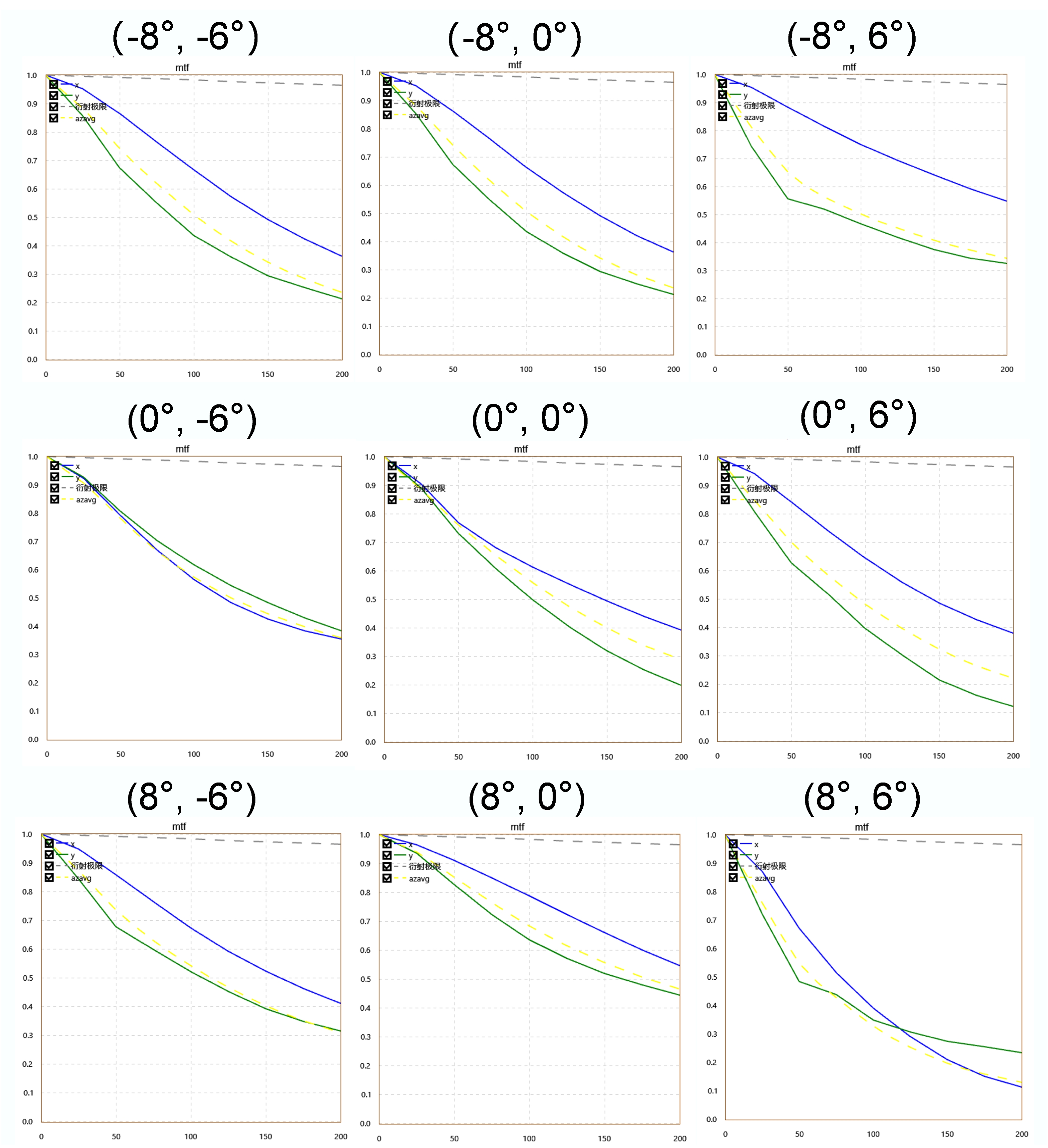
The design of conformal optical systems often suffers from insufficient theoretical guidance, resulting in repeated trial-and-error optimization. To address this, we introduce a design method based on aberration theory for plane-symmetric systems. By converting global surface parameters into local surface parameters, the aberration theory is generalized to conformal systems, enabling analytical calculation of each surface’s aberration contribution. Using this formulation, we propose a two-step design strategy. First, the optimal gimbal position is determined by minimizing the aberration contribution of the dome’s outer surface. Second, during arch-corrector optimization, freeform parameters associated with dominant aberrations are progressively introduced, and an aberration-coefficient-based merit function is employed. To validate the effectiveness of the proposed method, comparative designs of 14 conformal systems were completed for identical specifications across different gimbal positions and optimization approaches. Results demonstrate that the system designed using our method achieves a full-field modulation transfer function (MTF) exceeding 0.4 at a spatial frequency of 42 lp/mm, with imaging quality approaching the diffraction limit—representing a 2.4× improvement over conventional design methods. This approach provides systematic theoretical guidance for the design of high-performance conformal optical systems.


The subaperture stitching method based on computer-generated holograms (CGH) is a common approach for measuring the surface profile of cylindrical mirrors. However, the stitching result suffers from distortion of low-frequency surface shape information. This is primarily caused by the cumulative amplification of errors and the inability of conventional aberration fitting methods (based on orthogonal polynomials) to effectively separate errors from the true surface figure. To address this issue, this paper proposes a novel method to compensate for and correct the low-frequency information of cylindrical mirror surface profiles. First, an initial stitching is performed using a successive subaperture stitching method based on Chebyshev polynomials. Next, the profile along the mirror's stitching direction (i.e., the generatrix direction) is measured independently to extract its low-frequency component. Finally, this low-frequency information is used to further fuse and correct the initial stitching result. Experimental validation was conducted on a cylindrical mirror with a clear aperture of 150 mm × 210 mm and a radius of curvature of 790.23 mm. The results demonstrate that the proposed method effectively corrects the generatrix direction profile of the cylindrical mirror. Compared to the full-aperture reference surface obtained via full-aperture CGH measurement, the root mean square (RMS) of the residual error for the stitching result is approximately


To satisfy the thermal deformation testing requirements of ceramic-based ultra-stable structures for space gravitational wave detection, and address the difficulty of verifying the measurement link prior to component fabrication, a ground-based vacuum interferometric measurement system operating within 1 mHz–0.1 Hz is developed in this paper. We use an equivalent 4J32 Invar sample for tests. It matches ceramic parts in geometry, interfaces and optical path. We calibrate thermal expansion and test displacement stability. We also decompose low-frequency noise systematically. In the experiment, the tested structure, fiber-optic measuring probe, reflector and temperature sensors are placed in a vacuum environment, and the natural cooling of the cavity is utilized to realize the overall thermal response calibration of the measurement link. Under mK-level steady-state temperature control, the Welch method is employed to acquire the amplitude spectral density of displacement noise, and a comparative analysis is conducted on the intrinsic noise of the interferometer, thermal equivalent noise and system comprehensive noise. The experimental results show that the relative deviation between the system comprehensive thermal expansion coefficient and the intrinsic value of Invar is about 8.3%, which can effectively characterize the overall thermal response of the measurement link. The amplitude spectral density of displacement noise of the system in the mHz band is approximately 26.6 nm/√Hz, and the consistency of long-period multi-segment steady-state measurement results is high, demonstrating high reliability. The intrinsic noise of the interferometer is about two orders of magnitude lower than the system comprehensive noise, and the thermal equivalent displacement noise converted from temperature fluctuation only accounts for 7.8%~14.1% of the system noise; both of them are far lower than the comprehensive measurement noise and do not constitute major interference. The proposed system and method complete the full measurement link verification and noise benchmark establishment, and can provide an equivalent verification foundation and reusable technical scheme for subsequent thermal deformation testing of ceramic-based ultra-stable structures.


To meet the demand for multifunctional polarization manipulation and dynamic tunability in terahertz devices, a dual-functional switchable chiral metasurface based on graphene carrier modulation is proposed. By changing the polarization state of the incident wave and continuously tuning the Fermi level of graphene through an external gate voltage, the structure can exhibit circular dichroism (CD) and linear dichroism (LD) responses, enabling switching between different polarization-selective absorption characteristics. Simulation results show that when the graphene Fermi level is 1 eV, the metasurface exhibits pronounced selective absorption for left- and right-handed circularly polarized waves at 2.65 THz, with a CD value reaching 0.89, and maintaining CD values above 0.6 within the frequency range of 1.97–3.44 THz. When the Fermi level decreases to 0.2 eV, a significant linear dichroism response appears at 1.91 THz, with an LD value of 0.75. Analysis of the electric field and surface current distributions reveals that the difference in the strength of electric resonances excited under different polarization states is the primary mechanism responsible for polarization-selective absorption. In addition, the proposed structure demonstrates good robustness against variations in the incident angle and structural parameters, indicating its potential applications in circular/linear dichroism detection, polarization control, and terahertz photonic devices.


To address the issues of insufficient adaptability in cross-view feature fusion and inadequate utilization of complementary information in existing dual-view X-ray security inspection image prohibited item detection methods, this paper proposes an improved dual-view fusion detection method combined with YOLOv11 (Dual View Fusion combined with YOLOv11, DVF-YOLOv11). The proposed method employs a parameter-shared dual-branch YOLOv11 backbone network to extract multi-scale features from the overlook-view and side-view images, respectively. A Cross-View Attention Fusion (CVAF) module is designed to adaptively enhance dual-view features through a cascaded mechanism of channel attention and spatial attention. An adaptive weight prediction network is introduced to dynamically adjust the fusion weights of each view, and is combined with channel compression convolution to form a dual-path fusion strategy. A joint loss function composed of feature preservation loss, complementarity loss, and weight balance loss is further designed to guide the fusion learning process. On the DvXray dataset, the proposed method achieves an mAP50 of 94.02% and an mAP50-95 of 79.41%, improving by 2.99% and 5.29%, respectively, over the single overlook-view baseline. Experimental results demonstrate that the proposed method improves the accuracy and robustness of prohibited item detection in dual-view X-ray security inspection images.


Objective: The magnetic field near the test masses in space-based gravitational-wave detection spacecraft cannot be measured in situ, and the accuracy of magnetic field reconstruction is strongly affected by the arrangement of magnetic sensors. To address this issue, this study investigates a magnetic sensor configuration optimization method under constrained installation conditions, aiming to improve the magnetic field reconstruction accuracy at the test mass locations. Methods: The magnetic sensor placement problem was formulated as a discrete combinatorial optimization problem. An improved Ivy algorithm-based magnetic sensor configuration optimization method, termed MSC-IVYA, was proposed. The method integrates feasible installation region discretization, default-configuration-based population initialization, dynamic neighborhood updating, and a cumulative fitness function designed for multiple random magnetic source models, thereby enabling efficient search under installation constraints. Simulation evaluations were conducted on two representative space-based gravitational-wave detectors, LISA Pathfinder and Taiji-2, using three magnetic field reconstruction methods: inverse distance weighting (IDW), Taylor expansion (TE), and multipole expansion (ME). Results: For LISA Pathfinder, under the default configuration, the average relative errors of TM1 were 593.74%, 508.04%, and 516.50% using IDW, ME, and TE, respectively. After optimization with MSC-IVYA, these errors were reduced to 390.39%, 357.55%, and 363.89%, respectively. In the Taiji-2 case, MSC-IVYA also achieved consistent improvement. For TM1, the reconstruction errors using IDW and ME decreased from 72.14% and 77.27% to 32.55% and 47.25%, respectively. For TM2, the errors using ME and TE decreased from 97.17% and 112.14% to 74.27% and 80.76%, respectively. Conclusion: Magnetic sensor configuration is an important design variable affecting the magnetic field reconstruction performance at the test mass locations. The proposed MSC-IVYA method can consistently improve magnetic field reconstruction accuracy under different mission conditions. It is particularly suitable for engineering scenarios with a limited number of magnetic sensors and constrained installation regions, and provides methodological support for the design of magnetic diagnostic systems in space-based gravitational-wave detection spacecraft.


To overcome the limitations of current technologies, including the slow switching speed, heat accumulation, and high power consumption of thermo-optic waveguide switches, the high transmission loss of electro-optic waveguide switches, and the complex feedback control, difficulty in large-scale array integration, and narrow operating bandwidth commonly found in traditional photonic integrated circuit (PIC) waveguide switches, to meet the future demands of on-chip all-optical switching technologies for optical switches with fast response, low power consumption, broad bandwidth, low cost, and large-scale array fabrication capabilities, this study investigates micro-electro-mechanical systems (MEMS) driven silicon-based waveguide optical switch devices. By integrating silicon photonic waveguide technology with MEMS technology, we designed and fabricated an electrostatically driven MEMS 2×2 silicon waveguide optical switch (silicon photonic MEMS switch) capable of routing optical signals. The monolithic integration of silicon photonic waveguides and MEMS microactuators on a silicon wafer was achieved using electron-beam lithography combined with complementary metal-oxide-semiconductor (CMOS) processes. With a footprint of 192 μm × 192 μm, the device successfully demonstrated 2×2 optical switching functionality. The switching response times were measured at 20 μs and 15 μs, with optical signal rise and fall times of 15 μs and 10 μs, respectively. At a wavelength of


For ultrashort laser pulses, accurately characterizing their temporal characteristics (temporal width and phase) is crucial for their generation and application. Self-referenced spectral interferometry (SRSI), first proposed in 2010, utilizes the measured light itself to generate suitable reference light through third-order nonlinear optical processes, and employs Fourier transform spectral interferometry algorithms to reconstruct the input pulse. It has the advantages of single-shot, accuracy, and high sensitivity. This article provides an overview of the implementation of SRSI from two main aspects: the optical path and the reconstruction algorithm. On the optical path level, from the earliest proposed self-referenced spectral interferometry based on cross-polarization wave generation (XPW-SRSI) to the self-referenced spectral interferometry based on transient grating effect (TG-SRSI) with a compact total reflection configuration, the sensitivity, wavelength coverage, and compactness of the implementation path have been continuously iteratively upgraded. On the algorithm level, from pulse reconstruction methods targeting near Fourier transform limits to reconstruction algorithms for large chirp pulses with temporal broadening exceeding twice the Fourier transform limit, three evolutionary paths are discussed: spectral stitching schemes, reconstruction schemes incorporating supervised deep learning, and neural networks without training embedded in physical forward models. The latter achieves single-shot accurate reconstruction in large chirp and high noise scenarios without any pre-training dataset. In the face of emerging new beam characterization demands, the temporal measurement of ultrashort laser pulses still require significant attention in the future.


To meet the high-resolution imaging requirements of space-based optical payloads and address the challenge of ensuring reliable bonding between detectors and structural frames under extreme environmental conditions, this paper proposes a collaborative optimization scheme for the bonding of detector assemblies. Firstly, in accordance with the space environmental adaptability requirements of optical payloads, a systematic comparison of the core performance characteristics of commonly used adhesives was conducted. Epoxy resin was adopted as the primary bonding agent to ensure rigid and dependable attachment between the imaging unit and the support frame, while silicone rubber was employed to provide stress-buffering capability, forming a composite adhesion architecture. Subsequently, a multiphysics coupled simulation model was developed to investigate the influences of static mechanical loads and PCB soldering thermal conduction (200°C) on the stress, strain, and displacement of the photosensitive surface of the device while achieving quantitative control of adhesive. Finally, the reliability and stability of the scheme were verified through environmental testing. The results demonstrate that the closed-loop design effectively resolves the challenge of high-precision assembly. Pre- and post-test inspection using a coordinate measuring machine confirmed a coplanarity precision of 0.019 mm, a linearity precision of


To accurately monitor methane emissions from point sources, this paper explores the use of a Fabry-Perot (F-P) interferometer as the spectroscopic element of a spatial imaging spectrometer, aiming to achieve both high spatial and high spectral resolution. The study focuses on constructing both theoretical and physical models of the F-P cavity to meet the technical requirements of methane point-source monitoring. First, an initial theoretical model of F-P cavity interference under ideal conditions is developed based on multi-beam interference theory. Building upon this, a corresponding geometric model is established by considering the effect of finite throughput aperture, from which a theoretical model under finite aperture conditions is derived. In addition, a more comprehensive theoretical framework is constructed by incorporating surface defect distribution functions to account for microscopic random inhomogeneities and curvature defects. In the physical model development, the F-P cavity is initially designed based on the ideal theoretical model to match the spectral characteristics of methane absorption. Using the finite-aperture theoretical model, the transmission intensity curve and its slope are analyzed, and the aperture size is precisely determined bases on the physical meaning of the slope. Subsequently, the physical model is further optimized by adjusting the wedge angle at the rear surface of the mirror. To meet specific spectral and technical targets, the allowable variation in the gap spacing between the two parallel mirrors is thoroughly analyzed, thereby defining the tolerance range for the cavity gap. Surface roughness, figure accuracy, and parallelism of the reflective surfaces are then specified according to surface defect considerations. Ultimately, the optimized F-P cavity achieves a spectral resolution of 0.29 nm, meeting the technical requirements for methane point-source monitoring. By constructing a comprehensive theoretical model and optimizing the physical design, this study enables the realization of both high spectral and spatial resolution, provides a theoretical foundation for applying F-P interferometers in spatial imaging spectrometry, and supports the advancement of high-precision spectral detection technologies.


During on-orbit operation, space cameras are exposed to complex thermal environments. Non-uniform variations in the structural temperature field can induce thermoelastic deformation, leading to line-of-sight (LOS) pointing deviations and significantly degrading imaging accuracy and stability. To address the insufficient robustness of the traditional Least Squares (LS) method in analyzing LOS pointing stability of space cameras under complex thermal conditions, this paper proposes a thermal line-of-sight pointing analysis method based on the Iteratively Reweighted Least Squares (IRLS) algorithm. First, a thermo-structural coupled model of the space camera is established to analyze the mapping relationship between temperature field variations and LOS pointing deviation. Then, the IRLS algorithm is introduced to perform robust estimation of model parameters. By constructing a weighted residual function, the influence of abnormal measurement data on parameter identification is effectively suppressed, thereby improving the prediction accuracy of thermal deformation. Meanwhile, an energy-iterative window adaptive centroiding algorithm is adopted to capture the variation of spot centroid positions with temperature changes. To investigate thermally induced pointing drift of the on-orbit camera, thermal experiments are conducted. Simulation results are further validated using ground-based thermal test data, and the performance of the proposed IRLS method is compared with that of the traditional LS method in terms of pointing error prediction accuracy and convergence characteristics. The results demonstrate that the proposed IRLS-based thermal analysis method significantly improves the prediction accuracy of LOS pointing deviation in the presence of measurement noise and outliers, while enhancing the stability and robustness of the model. This approach provides an effective technical solution for on-orbit thermal deformation compensation and accuracy maintenance of high-resolution space cameras.


In real-time brain neural observation of freely moving animals, the miniature head-mounted fluorescence microscope is currently one of the most advanced brain science observation instruments. However, most existing miniature fluorescence microscopes, in order to meet strict size and weight constraints, have a limited field of view, making it impossible to simultaneously observe neural activity in multiple brain regions. On the other hand, a few products with a larger field of view are too heavy to be worn on small animals. This study employs lightweight, planar, and high-quality gradient refractive index lenses to reduce the microscope's weight while ensuring a large field of view. Using gradient refractive index lenses for the design of a large-field-of-view miniature fluorescence microscope, this research derives the off-axis aberration formula for oblique light incidence on gradient refractive index lenses, analyzes the refractive index distribution model and aberration correction of these lenses, and designs a miniature fluorescence microscope with a 4 mm×4 mm field of view, a numerical aperture (NA) of 0.1, and a prototype weight of only 2.89 g. The central visual field resolution is 13.9 μm, preliminarily achieving the resolution for neural cells in freely moving mice.


Aiming at the problem that existing spectral compressed sensing algorithms adapted to the visible band are difficult to achieve high-precision reconstruction for sharp gas absorption features in the mid-wave infrared (MWIR) spectra, this paper proposes a physics-driven MWIR spectral compressed encoding and reconstruction network to realize high-precision reconstruction of MWIR spectra with sharp gas absorption features. The dual-branch MWIR spectral reconstruction network serves as the core module of the proposed framework. Specifically, the network consists of two parallel branches, namely the smooth background reconstruction branch and the characteristic absorption reconstruction branch, which respectively realize the accurate reconstruction of smooth background logarithmic spectrum and sharp gas characteristic absorbance. Subsequently, high-accuracy reconstruction of MWIR gas absorption spectra is achieved through information fusion, physical quantity conversion, and post-processing with fully connected layers. Experimental results on the reconstruction of gas absorption spectra within the 3.7−4.8 μm band with 45 channels in real-world scenarios demonstrate that the proposed method achieves a peak signal-to-noise ratio (PSNR) of more than 28.159 dB and a spectral angle mapper (SAM) value of better than 0.053 rad. For a data cube with an image resolution of 320×256, the reconstruction time is approximately 0.65 seconds. This method effectively breaks through the technical bottleneck of high-precision MWIR spectral reconstruction, and it features both the interpretability of physics-driven models and the generalization capability of data-driven models. It provides a feasible technical path for MWIR spectral compressed sensing and exhibits significant potential for practical applications.


To address the low optical efficiency in the peripheral regions of large-scale solar power tower heliostat fields, this study proposes an overlapping layout optimization method and a multi-target aiming strategy for triple-tower solar thermal power plants. First, Particle Swarm Optimization (PSO) is utilized to determine the optimal configuration for a single-tower layout. These individual fields are then arranged, and the optimal overlapping triple-tower layout is established by refining the inter-tower distances. Finally, a multi-target aiming strategy is implemented for heliostats within the overlapping zones based on their instantaneous optical efficiency. By modeling the solar concentration process and comparing layout configurations, the results demonstrate that the annual average optical efficiency of the overlapping triple-tower field is 0.24% higher than that of the distributed counterpart. Furthermore, the overlapping arrangement is more compact, resulting in a significantly reduced land footprint.


Space-based gravitational wave detection uses laser heterodyne interferometry to measure picometer-level displacement fluctuations of test masses separated by millions of kilometers. The interferometric system must achieve picometer-level accuracy in the millihertz frequency band. In the interferometer, test-mass rotation limits system sensitivity through two types of coupling errors: rotation–rotation coupling and rotation–translation coupling. This paper systematically investigates the mechanisms of these two errors and adopts a sequential suppression strategy: rotation–rotation coupling is first suppressed, followed by rotation–translation coupling.A test-mass interferometer is developed based on laser heterodyne interferometry and wavefront sensing, enabling high-sensitivity displacement and angular measurement as well as noise analysis. The coordinate transformation between the steering mirror and the detector is experimentally calibrated. The steering mirror is then rotated to the minimum-coupling angle, aligning the two coordinate systems and suppressing rotation–rotation coupling. An optical model is further established based on geometric relationships, and its parameters are experimentally calibrated. A real-time compensation system is developed to dynamically suppress rotation–translation coupling.After suppression, the rotation–rotation coupling coefficient is approximately 12.5 mrad/rad. The rotation–translation coupling error is reduced by about 90% in the time domain and by approximately one order of magnitude in the frequency domain. These results provide a theoretical and experimental foundation for multi-degree-of-freedom decoupling and noise suppression in interferometers for space-based gravitational wave detection.


To overcome the formidable challenges of suppressing laser frequency noise and clock noise in millihertz-band space-borne gravitational wave detection, as well as the inherent complexity and limitations of conventional second-generation Time-Delay Interferometry (TDI) schemes, this study proposes an innovative payload architecture and noise suppression strategy based on Space-borne Optical Clocks (SOCs). We first detail the core payload design, which replaces the traditional Ultra-Stable Oscillator (USO) on each spacecraft with an advanced SOC system. Subsequently, we introduce two synergistic noise suppression mechanisms: locking the laser strictly to atomic transition frequencies, and employing optical frequency combs (OFCs) to down-convert the optical clock frequency into a highly stable microwave clock signal. Drawing upon the stability parameters of state-of-the-art SOCs, the system's noise suppression performance across the target frequency band of 0.1 mHz to 1 Hz is comprehensively verified through both theoretical analysis and numerical simulations. The results demonstrate that the proposed scheme suppresses laser frequency noise and clock noise by two and three orders of magnitude in the millihertz band, respectively, ensuring that the residual noises remain well below the stringent noise floor required for the mission. Remarkably, this architecture enables the first-generation TDI technology to fully satisfy the mission requirements, thereby eliminating the need for additional complex clock-noise-removal algorithms. Consequently, while preserving high detection sensitivity, this scheme drastically enhances the simplicity and robustness of the data processing pipeline, and significantly relaxes the rigorous precision constraints typically imposed on inter-spacecraft ranging and clock synchronization. As SOC technology continues toward miniaturization, the proposed framework exhibits substantial application potential for future space-borne gravitational wave observatories.


In space-based gravitational wave detection, the Point-Ahead Angle Mechanism (PAAM) is crucial for high-precision pointing of intersatellite laser links, but its rotation introduces tilt-to-length (TTL) noise that severely limits interferometric accuracy. To suppress local TTL noise caused by PAAM angular jitter, this paper proposes an imaging system that optically images the detector onto the equivalent rotation center of the PAAM, actively mitigating geometric TTL noise. A highly symmetric equal-arm heterodyne interferometer test platform was constructed, and IFOCAD simulations were performed to evaluate suppression performance under non-ideal conditions (angular jitter, rotation center offset, installation errors, thermal deformation). Results show that under ideal alignment, the imaging system suppresses 98.9% of lever-effect optical path changes and 98.2% of piston-effect changes. With installation errors, TTL noise is suppressed within


This paper studies the phase meter applied to space laser interferometry. The phase-locked loop will suffer from lock loss in actual operation. Researchers commonly adopt the FFT frequency measurement method to re-acquire the signal at the present stage. This method has obvious technical defects. Its frequency measurement accuracy is low at the order of 100 Hz, and the relocking time is long about 7 ms. This paper proposes an automatic relocking technique deployed in collaboration with FFT. This technique adopts a lock-loss detection strategy that combines instantaneous frequency values and frequency change rates. It selects two data sources to judge lock loss, including the original data of the loop filter and the down-sampled data of CIC. It clears the integration error through the reset operation after lock loss occurs, and it receives the predicted value output by the frequency prediction algorithm. The frequency prediction algorithm uses the waveform generation algorithm for periodic signals. It uses the second-order polynomial prediction algorithm for aperiodic signals. It also combines interpolation technology to generate the corresponding frequency predicted value. The automatic relocking technique and FFT are deployed in parallel, and they form a clear functional division. This technique performs frequency prediction based on the inherent regularity of the signal. It deals with lock-loss scenarios of all regular signals regardless of the lock-loss duration. It also realizes fast relocking of short-time irregular signals within 1 s. FFT is responsible for signal re-acquisition in irregular signal scenarios and long-time complex lock-loss scenarios. The two methods form a working mode with complementary advantages. Experimental verification results show that the algorithm proposed in this study has an average relocking time of 32 μs and a maximum relocking time of 60 μs in the scenario of regular signal lock loss. The performance is improved by two orders of magnitude compared with the FFT method. The relocking speed has no correlation with the lock-loss duration. It can still maintain the relocking speed at the order of tens of microseconds when the lock-loss duration reaches 10 s. The frequency estimation error is stably controlled below 10 Hz in the signal-to-noise ratio range from −10 dB to 10 dB. The system can still achieve stable locking even when the signal-to-noise ratio is as low as −10 dB. This architecture deployed in collaboration with FFT retains the wide-band acquisition capability of FFT. It significantly improves the fast relocking capability in regular signal scenarios. It provides high-precision, fast-response and high-stability phase measurement technical support for space gravitational wave detection missions.


Due to the in-situ antagonism and site competition during multi-ion coexistence in real water environments, traditional linear sensing models often fail. In this study, nitrogen-doped carbon dots (N-CDs) synthesized via a one-step hydrothermal method were used as a platform to investigate the microscopic response mechanism in Cu2+ and Fe3+ coexisting systems by constructing a 2D cross-fluorescence response matrix. Firstly, the fluorescence quenching evolution under different interference backgrounds was experimentally observed. The results showed that under a high concentration Cu2+ background, the fluorescence response induced by Fe3+ exhibited significant nonlinear shifts and quenching stagnation, confirming the intense exclusive competition between the two ions at the nano-interface. Subsequently, to analyze this nonlinear process, a "four-state physical kinetic model" was constructed based on the principle of detailed balance, and a global response analytical expression containing the thermodynamic synergy factor (


Weak measurement technique based on weak-value amplification offers an effective method to detect the tiny spin splitting in the photonic spin Hall effect. However, its performance is constrained under conditions of strong coupling or near-orthogonality between the pre- and post-selected states. Based on differential interference theory, this work establishes a relation between the spin-dependent displacement and the amplified displacement for vortex beam with arbitrary topological charge under partial reflection at an air–glass interface. The relation remains valid even under strong-coupling conditions or when the pre- and post-selected states are nearly orthogonal, and is applicable for arbitrary incident linear polarizations. The corresponding characteristics of vortex beam reflected at an air–glass interface is systematically analyzed, and the influences of key parameters including the incident angle, topological charge, incident polarization state, post-selection angle, and propagation distance on the amplified displacement are elucidated. This study provides a valuable theoretical foundation for the applications of vortex beam in precision optical measurement and optical micromanipulation.


Dispersion scan (D-scan) is an ultrashort laser pulse characterization technique based on dispersion modulation and nonlinear spectral response, and, owing to its extremely simple optical configuration and high sensitivity to broadband spectra and phase evolution, it has developed into an important tool in the field of ultrashort pulse characterization. Focusing on the ability of D-scan to meet the demands of real-time operation and robustness, as well as its extension toward extreme parameters such as single-cycle pulses and the deep-ultraviolet region, this paper systematically reviews the key progress of D-scan technology in terms of retrieval algorithm optimization and experimental scheme expansion. First, the evolution of D-scan retrieval algorithms is summarized. This progression traces the shift from early Nelder–Mead and differential evolution algorithms to the current standard generalized pulse retrieval algorithm, and ultimately to deep-learning-based techniques that enable millisecond-level, real-time reconstruction. Particular emphasis is placed on the improvements in computational speed, algorithmic robustness, and noise immunity achieved across these diverse approaches. Regarding experimental techniques, the paper examines second-harmonic-generation (SHG) D-scans based on second-order nonlinearities. It details the technological transition from conventional scanning methods to real-time, single-shot measurements, and highlights recent progress in applying SHG D-scans to vectorial optical field characterization. Subsequently, to circumvent the physical limitations of second-order nonlinearities—specifically concerning multi-octave spectral overlap and phase matching in the DUV region—this review further explores D-scan techniques leveraging third-order nonlinear effects and their derivatives. It elucidates how these methodologies push the application boundaries of D-scan toward the single-cycle limit and into the DUV regime. Finally, current challenges confronting D-scan technology are outlined, including its reliance on external components and its extension to longer wavelengths and longer pulse durations. The paper concludes with an outlook on the future trajectory of D-scan technology within strong-field physics and attosecond science.


To enable low-cost and efficient characterization of EUV photoresists, a lithographic evaluation system based on a tabletop high-harmonic generation (HHG) source and a reflective interferometer was developed. High-order harmonics were generated in argon using a 515 nm femtosecond laser. After focusing by a toroidal mirror and spectral dispersion by a blazed grating, the 11th harmonic (46.8 nm) was selected through a slit as the EUV source. Nonchemically amplified resists based on oxime sulfonate-functionalized polystyrene (PSOS) were used as the test material, and interference exposure was performed with a Lloyd’s mirror and a symmetric dual-mirror configuration. To solve the alignment problem between the sample plane and the symmetric dual-mirror interferometer, an optical ranging method based on diffraction-fringe inversion was proposed, enabling precise positioning of the symmetric dual-mirror interferometer. The results show that the Lloyd’s mirror produces clear high-contrast line-space patterns with a period of 125 nm and enables characterization of the tested resist at the 100 nm scale. After precise positioning by diffraction-fringe inversion, the symmetric dual-mirror configuration produces line-space patterns with a period of 60 nm, significantly improving the system resolution. This evaluation system provides a low-cost and scalable experimental platform for rapid screening of photoresist materials, investigation of resolution limits, and development of related lithographic processes.


To achieve the generation of ultrashort isolated attosecond pulses using few-cycle pulses, it is necessary to study the precise control of the electric field of few-cycle light through double optical gating technology. In conventional experiments, double optical gating typically regulates multi-cycle pulses, and the analysis does not consider higher-order dispersion during laser propagation in media, second-harmonic conversion efficiency, or the exact waveform of the second-harmonic electric field. However, such approximations are no longer valid for few-cycle pulses. This paper accurately simulates the propagation and second-harmonic generation process of few-cycle pulses in nonlinear crystals based on a coupled-wave equation model, revealing the key influence of dispersion effects and other factors on the gating waveform. The research shows that when the driving light field is a few-cycle laser pulse, the traditional electric field estimation method for double optical gating is no longer applicable. Few-cycle pulse lasers have an ultra-broad spectrum, and effects such as group velocity mismatch, phase mismatch, and dispersion caused by differences in phase accumulation among different wavelength components become significantly more pronounced compared to long pulses. For a few cycle pulse, the optimal gating light field can be achieved by adjusting the thickness of the beta-barium borate (BBO) crystal in the double optical gating setup to 126.4 μm. This paper proposes that coordinated adjustment of the waveplate and BBO crystal thickness can finely tune the relative delay between the driving field and the second-harmonic field, thereby optimizing the gating electric field and the driving electric field, providing effective parameter optimization guidance for the generation of ultrashort isolated attosecond pulses.


With the advancement of photoelectric technology, optical films are extensively employed in military, medical, and communication fields. Film thickness is a critical parameter that determines optical performance, and the accuracy of its monitoring system directly affects spectral characteristics. To mitigate the significant thickness control errors in conventional direct monitoring systems—caused by light source divergence and weak detector response signals—this paper proposes an externalized optical configuration. In this design, both the optical transmitter and receiver are placed outside the vacuum chamber, thereby avoiding interference from chamber vibration, temperature variations, and assembly inconsistencies. Additionally, an optical signal modulation scheme based on fiber coupling and collimation-focusing is introduced. By adopting an external integrated light source combined with multimode optical fibers and a composite optical path, and by optimizing component parameters through optical simulation to improve spot quality and energy density, the stability of both optical and electrical signals is enhanced. After optimization, irradiance at the fiber receiving end increased by 222.7%, signal strength by 156.6%, and the signal-to-noise ratio by 70.38%. The system’s performance was validated by preparing a narrowband filter film with a center wavelength of


Single-frame image deblurring remains an inherently ill-posed problem. Furthermore, existing diffusion models suffer from high inference latency, while state space models lack sufficient cross-modal interaction capabilities. To overcome these limitations, we propose an end-to-end Event-fusion Multi-head Attention Network (EFMAN) that exploits high-frequency spatiotemporal priors from event cameras for high-quality image restoration. Specifically, a cross-modal adaptive attention mechanism is designed to precisely align asynchronous high-frequency event streams with synchronous RGB features in both spatial and temporal dimensions, thereby compensating for exposure deficiencies. To mitigate the impact of inherent sensor noise, a Feature Enhancement Attention (FEA) module bolsters feature robustness against noise via global context modeling. Additionally, a Lightweight Channel-Spatial Attention (LCSA) module is integrated to adaptively recalibrate feature responses while substantially alleviating computational redundancy. These components are optimized by a multidimensional joint loss function—encompassing pixel, feature, and gradient domains—to synergistically enforce multi-scale constraints, ensuring consistency between micro-textures and global topologies. Extensive experiments demonstrate that EFMAN significantly enhances deblurring performance while maintaining efficient inference. Compared to state-of-the-art methods, our approach achieves maximum PSNR and SSIM improvements of 1.19 dB and 0.005 on the GoPro dataset, and 0.38 dB and 0.003 on the REBlur dataset, respectively. By effectively addressing the challenges of multi-modal alignment and noise interference, EFMAN strikes an optimal balance between restoration quality and computational efficiency, making it highly suitable for clear image reconstruction in high-dynamic-range and rapid-motion scenarios.


The microwave photonic filter based on weighted delay structure simultaneously leverages the advantages of photonic and radio-frequency components, featuring reconfigurability, low cost, and wide bandwidth, providing flexible and efficient signal processing capabilities in the microwave band. However, due to the complexity of the weighted delay structure, discrete optoelectronic components in the system can interfere with the weighted taps at different wavelengths—such as the envelope and gain competition of optical frequency combs, the gain non-uniformity and nonlinearity of EDFA, and the limited filtering bandwidth of modulators. These factors cause deviations in the weighted taps from their designed values, leading to distortion in the microwave filter. This paper proposes an end-to-end optimization approach by treating the microwave photonic filter as a black-box system. By monitoring the spectral shape (i.e., the weight values of each tap) of the final output in real time, the difference between the wavelength taps and the ideal taps is calculated and feedbacked to adjust the filtering coefficients of the waveshaper in real time, ensuring the output spectral weights remain in the designed state. Through this end-to-end optimization approach, we achieved a spectral reconstruction accuracy of 0.05dB and completed an RF low-pass filter with an out-of-band rejection ratio of up to 47dB.


Objective: To retrieve the pulse information from the dispersion scanning (d-scan) trace, a differential evolution (DE) algorithm is used. Methods: A partially coherent pulse train is generated and then test by traditional DE algorithm and its improved version. Results: The errors retrieved using the traditional and improved DE algorithms are 7% and 1%, respectively. Conclusion: The improved algorithm can more accurately retrieve the d-scan trace of partially coherent pulse train.


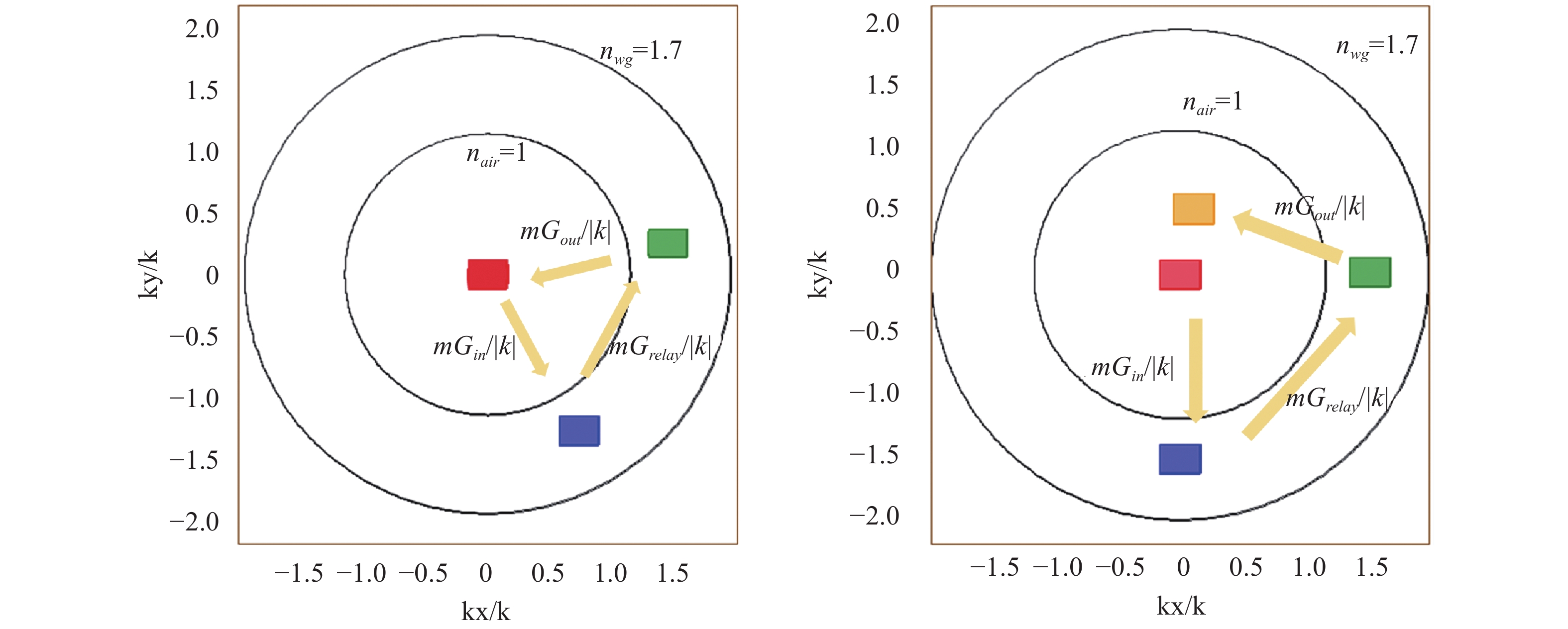
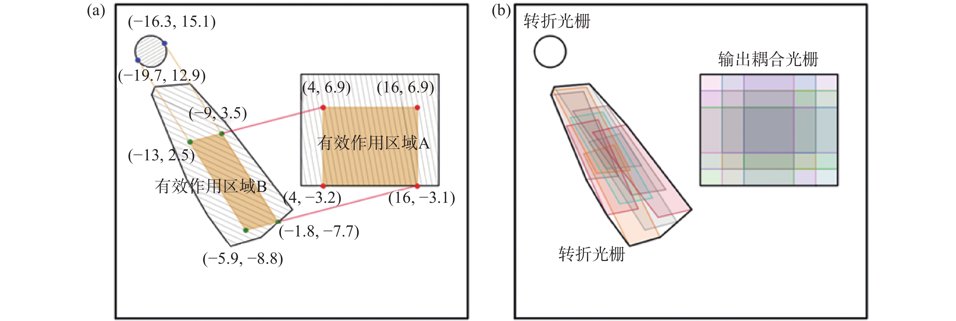
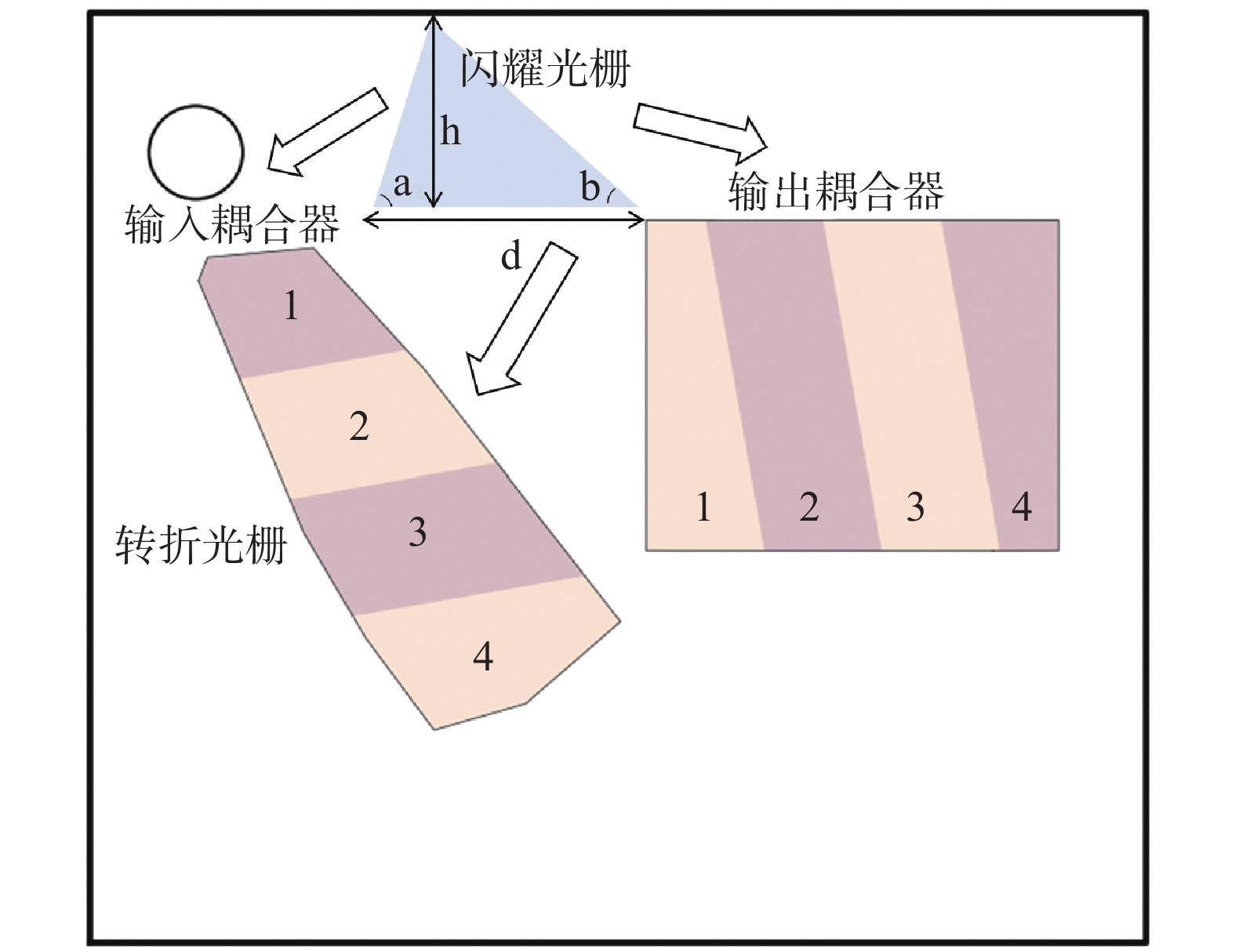
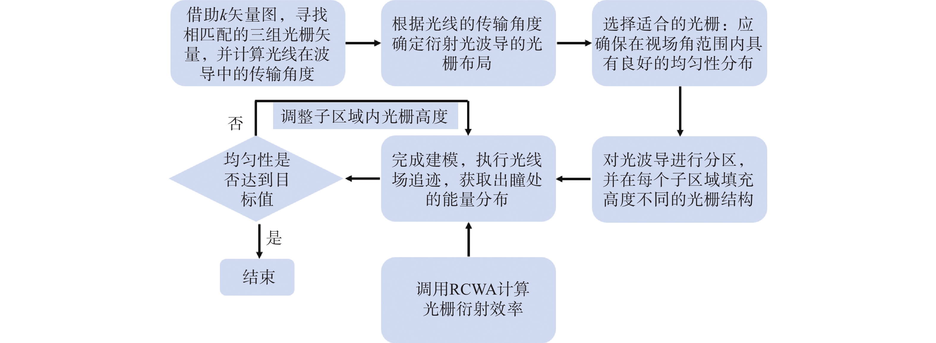
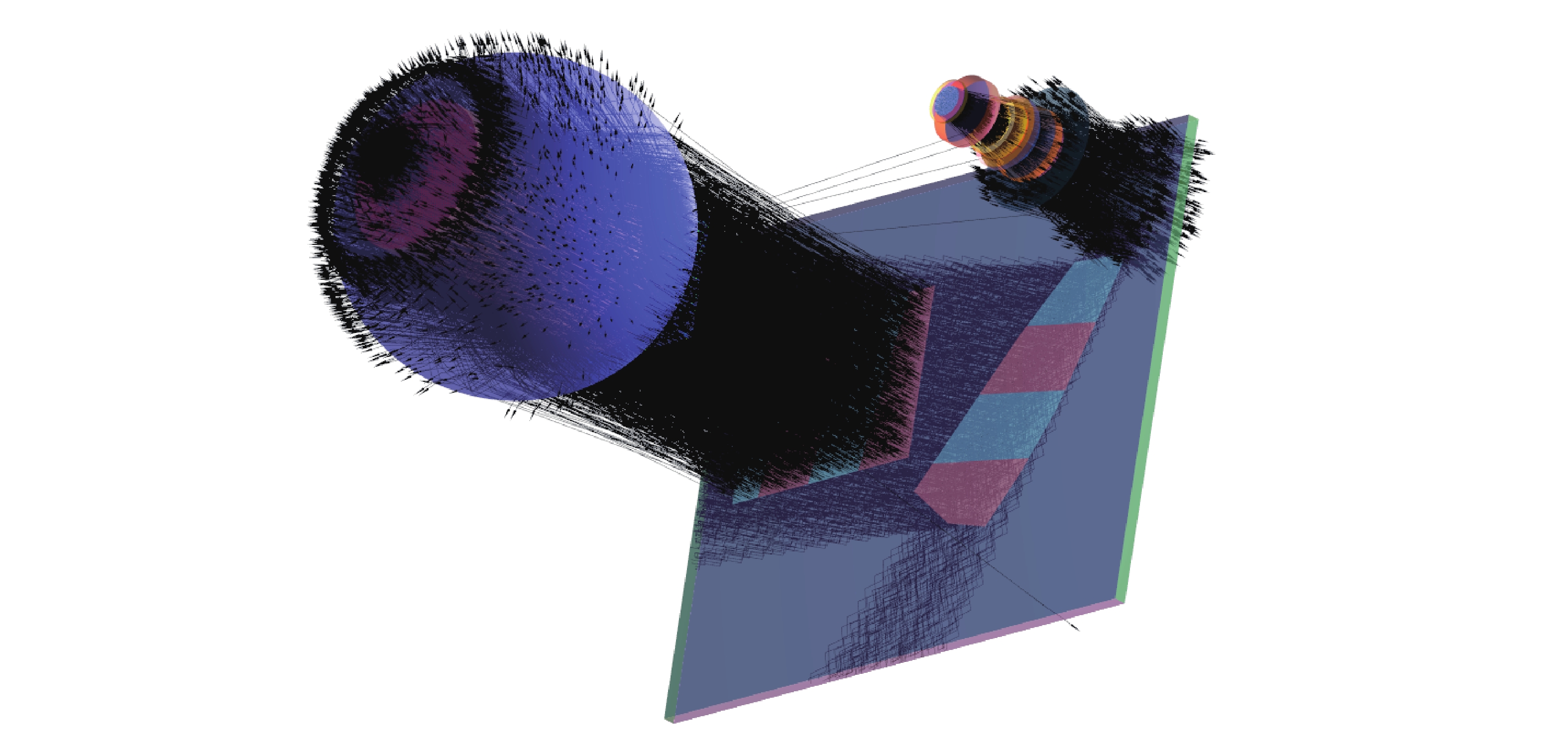
Diffractive waveguides have emerged as a particularly promising solution for augmented reality (AR) near-eye display technologies. These waveguides are characterized by their light weight, wide field of view, and large eyebox. However, most commercially available AR waveguide simulation software has been developed by foreign companies, and there has been little advancement in domestic 3D visualization software for optical waveguide design and simulation. The present study is, to the best of our knowledge, the first to develop 3D visualization module for optical waveguide design and simulation based on ray-field tracing. Using this module, a two-dimensional exit-pupil-expansion diffractive waveguide has been designed, and a systematic design workflow is demonstrated. The workflow integrates